Also at ]Department of Physics, University of Wisconsin-Madison.
Upscaling High-Quality CVD Graphene Devices to 100 Micron-Scale and Beyond
Abstract
We describe a method for transferring ultra large-scale CVD-grown graphene sheets. These samples can be fabricated as large as several and are characterized by magneto-transport measurements on SiO2 substrates. The process we have developed is highly effective and limits damage to the graphene all the way through metal liftoff, as shown in carrier mobility measurements and the observation of the quantum Hall effect. The charge-neutral point is shown to move drastically to near-zero gate voltage after a 2-step post-fabrication annealing process, which also allows for greatly diminished hysteresis.
pacs:
72.80.Vp, 81.05.ue.Graphene is well-known for its desirable electrical properties, Neto et al. (2009) and with all of the intense focus on research in the material, new applications are being constantly discovered. While graphene is known to have its best electrical properties when it is single-crystalline and suspended, Bolotin et al. (2008); Du et al. (2008) those attributes are currently not feasible for mass-produced devices. There have been very exciting developments related to improving non-suspended graphene’s mobility on more exotic substrates such as hBN, Dean et al. (2010); Banszerus et al. (2015) as well as improving the chemical vapor deposition (CVD) growth process for producing better quality devices with large grain sizes. Petrone et al. (2012); Yan et al. (2012); Banszerus et al. (2015) However, these developments are currently difficult to scale up and automate.
On the other hand, CVD-grown graphene is still the best way to repeatably produce large areas of monolayer graphene, and SiO2 is a well-known substrate that is already integrated into many processes from semiconductor physics to MEMS, Bunch et al. (2007); Zang et al. (2015) and beyond. Previous work has shown how to transfer large areas of CVD-grown graphene onto arbitrary substrates Liang et al. (2011); Suk et al. (2011); Song et al. (2013); Pimenta et al. (2014) and remove contaminants. Liang et al. (2011); Her, Beams, and Novotny (2013) However, previous CVD-grown graphene on SiO2 devices do not combine the desirable properties of high enough quality electrical characteristics to display the quantum Hall effect (QHE), a charge neutral point (CNP) near zero gate voltage, and a large device size, with typical finished devices being on the order of . Sun et al. (2014) Large-scale integration of easily manufactured, high-quality graphene devices is desirable in many different applications, such as graphene transistors, broad-band optical modulators Liu et al. (2011) and antennas. Tantiwanichapan et al. (2013)
Challenges arise when fabricating high-quality CVD-grown graphene devices, primarily due to contaminants of all kinds easily attaching to graphene. With each step, much care must be taken to remove any existing organic or inorganic contaminants on the graphene as well as prevent new contaminants from being attached. This paper presents a fabrication method that produces devices with CVD-grown graphene on SiO2 that are hundreds of microns in size and display the QHE.
A sheet of copper is supplied with CVD-grown graphene on only one side. Other sources of CVD graphene on copper typically have graphene on both sides of the foil, and in that case an oxygen plasma can be used to remove graphene from one side. A wet transfer process is used to place the graphene on the substrate, with cleaning steps to remove inorganic and organic contaminants from the bottom of the graphene before transfer. These steps are similar to the method detailed by Liang et al., which itself includes a “modified RCA clean” process. Liang et al. (2011)
It is important to be sure that all contaminants from the graphene are removed, as any resist residues can act as dopants and scattering centers to degrade electrical performance Bolotin et al. (2008); Du et al. (2008) as well as increase contact resistance. Li et al. (2013); Lee et al. (2013) Acetone or other common solvents are not sufficient to remove residues from resists such as poly(methyl methacrylate) (PMMA). A common technique to clean small graphene devices is to use current annealing, Moser, Barreiro, and Bachtold (2007) especially when the graphene is suspended, as it can effectively evaporate many contaminants and allow the graphene to self-heal. Barreiro et al. (2013) Other cleaning methods include mechanical cleaning with atomic force microscopy, Goossens et al. (2012) exposure to ultra-violet light, Chen et al. (2012) ozone treatment, Chen et al. (2012); Li et al. (2013) and annealing in vacuum Pirkle et al. (2011) or with gas flow. Ishigami et al. (2007) In the process detailed in this paper, the graphene is cleaned before transfer to a clean substrate, and then cleaned again after fabrication by a 2-step thermal annealing process.
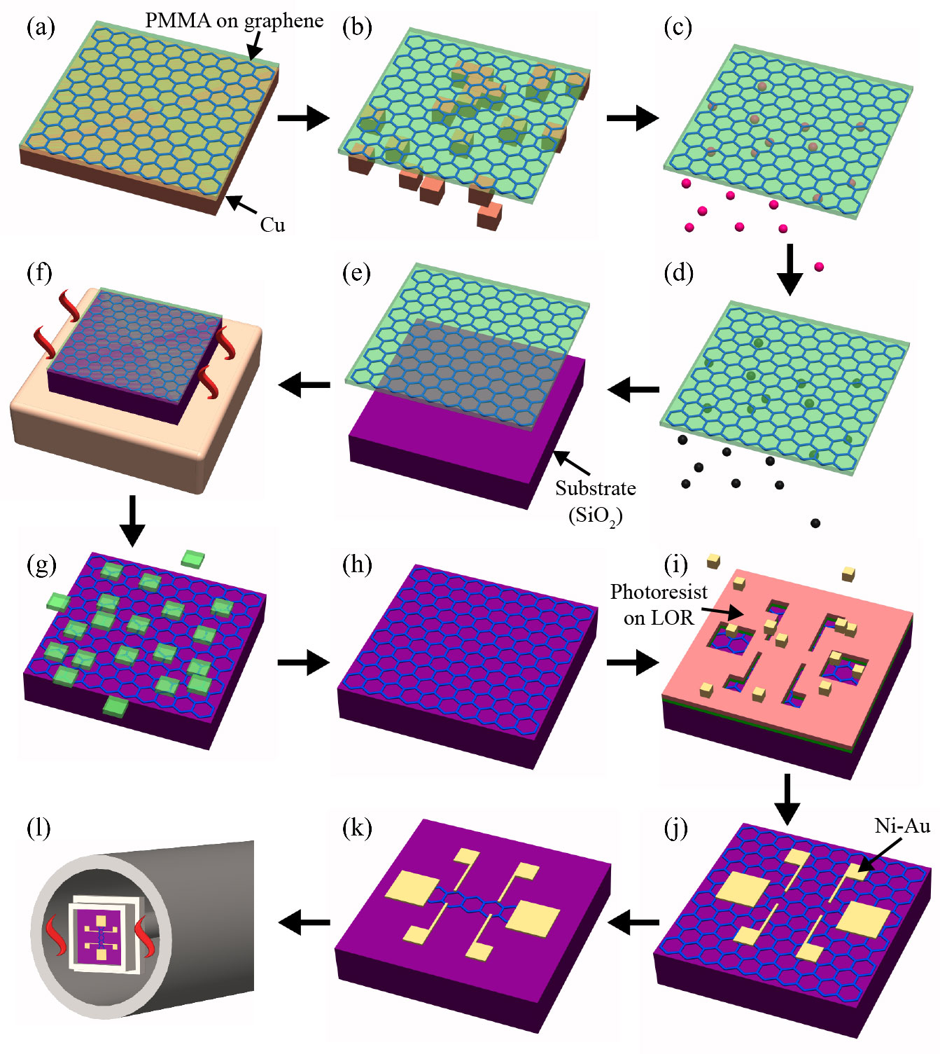
The size of the graphene/copper foil pieces used here is , however, the process can easily be upscaled to sizes of several . PMMA with a molecular weight of 950K is spun onto the graphene/copper foil and dried by air (Fig. 1(a)). A solution of Fe(NO3)3 is prepared with / of DI water and the PMMA/graphene/copper stack is placed to float in the solution with the copper side down, then left for at least 10 hours for the copper to etch away (Fig. 1(b)). Subsequently, the graphene stack is transferred to clean DI water at least twice, waiting 5 minutes after each transfer. Similarly to Liang et al., the RCA clean step referred to as Standard Clean 2 is next, with a HCl/H2O2/H2O solution prepared in a 1:1:20 ratio. Once again, the stack is placed on this solution to clean inorganic contaminants not removed by the Fe(NO3)3, such as oxides, for 15 minutes (Fig. 1(c)). The stack is then once again transferred to clean beakers of DI water at least twice for 5 minutes each. Finally, the RCA clean step known as Standard Clean 1 (SC-1) is performed with a NH4OH/H2O2/H2O solution in a 1:1:100 ratio for 5 minutes (Fig. 1(d)) to remove organic contaminants. The cleaning time and chemical concentrations of H2O2 and NH4OH in SC-1 are lower than reported in the modified RCA clean process in order to avoid bubble formation. Bubbles that get under the graphene stack can lead to the graphene tearing and are very difficult to remove before transfer. After the SC-1 step is complete, the graphene is again transferred to clean beakers of DI-water twice, waiting 5 minutes after each transfer.
Wafers of thermally grown SiO2 on -doped Si are prepared by carefully cutting into appropriately sized pieces with a diamond scribe. Any contaminants are cleaned off with sonication in acetone and then isopropanol before the wafers are dried with a N2 gun. The SiO2 is then treated with O2 plasma in order to make the surface more hydrophilic Nagashio et al. (2011), so the graphene will stick to it more readily and minimize breakage. Within one minute of the substrate’s O2 plasma exposure, the PMMA/graphene stack is scooped up and it is all dried in an oven set to for 15 minutes (Fig. 1(e) and (f)). Finally, the PMMA is removed with acetic acid (Fig. 1(g)), which more cleanly removes PMMA residue than acetone, while at the same time not attacking either the graphene or the SiO2 substrate. Her, Beams, and Novotny (2013) At this point, the graphene is cleanly transferred to the substrate with minimal cracks or tears (Fig. 1(h)), with most defects existing previous to the transfer process. Many other defects can be explained by bumps, folds, or other surface features in the copper foil that the graphene was grown on. These features make it much less likely for the graphene to transfer tear-free, making it very important to keep the copper foil as flat as possible. As shown in Fig. 2(a) and 2(b), Raman spectra at were taken in multiple locations to verify reproducibility of the measurement and uniformity of the graphene monolayer.
Once the graphene is on the target substrate, it must still have metal contacts deposited as well as be patterned into whatever shape is desired. Both of these steps must ideally be done without damaging or contaminating the graphene any more than absolutely necessary. The contacts are defined using photolithography, with a layer of Microchem LOR 5A used between the photoresist and graphene. This bi-layer stack tends to remove much more cleanly than photoresist alone Nath et al. (2014) and after removal can result in high-quality devices. In our observation, it also results in a higher final yield of usable devices due to less undesired graphene removal during liftoff. Without a protective layer of LOR, negative photoresists tended to result in much worse yield than positive resists, possibly due to crosslinking of polymer chains during exposure. After exposure and development, a layer of Ni is deposited by physical vapor deposition as an adhesion layer, followed by of Au (Fig. 1(i)). Liftoff is then performed in a two-phase process. First, the sample is soaked in a bath of acetone, which removes the photoresist and lifts off the excess metal. Since an ultrasonic bath will damage the graphene, excess metal is instead gently removed by squeezing a pipette to agitate the acetone. Second, after all excess metal is removed, the LOR layer is removed by being soaked in Microposit Remover 1165 for five minutes. Finally, the sample is rinsed with isopropanol and dried with a N2 gun. The result is shown in Fig. 1(j).
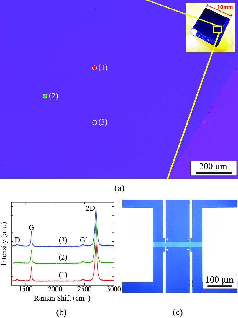
For this sample, excess graphene is removed by using photolithography to cover the areas of graphene to be protected from O2 plasma. The sample is then chemically cleaned for the final time with acetone and isopropanol, then dried with N2. Fig. 1(k) and 2(c) show the final result.
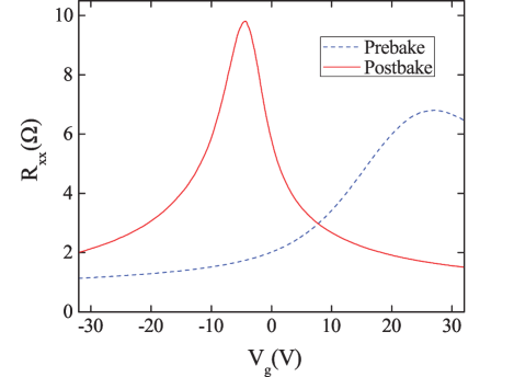
The sample is then mounted in a probe with air pumped out and replaced with a small quantity of He as an exchange gas. The longitudinal resistance is measured over a range of applied gate voltages at a temperature of at zero magnetic field. The sample is annealed under vacuum for 16 hours at to remove all water, including water trapped between the graphene and substrate. The sample is then removed from vacuum and quickly mounted in a probe, and once again annealed in a tube oven under vacuum (Fig. 1(l)) at for 72 hours to remove any water absorbed from the atmosphere during mounting. During this time, the 2-point resistance of the Hall bar is observed to steadily increase from approximately to a new maximum of . Fig. 3 shows the increase in peak longitudinal resistance along with a dramatic shift of the charge neutral point (CNP) from = to before and after annealing, respectively, which is evidential of the concentration of charged impurities being significantly reduced. Adam et al. (2007) The large peak shift is indicative of the removal of a majority of -type dopants such as water Novoselov et al. (2004) and the settling of the CNP at a negative gate voltage may be due to doping by the metal contacts or contact doping by SiO2 and any contaminants trapped between the graphene and metal during processing. Giovannetti et al. (2008); Nagashio and Toriumi (2011) When the sample is re-exposed to atmosphere, the CNP drifts toward the prebake value, though performing the baking process once more moves the CNP back to near-zero gate voltage. Thus, a capping layer is necessary to prevent adsorbates from altering the electrical characteristics of the graphene when exposed to air.
The CNP changes by at most , depending on the direction the gate voltage is swept. When there is still a significant amount of water on the substrate, this hysteresis can easily be on the order of a few or even tens of volts. Nagashio et al. (2011) This effect is typical of graphene on SiO2 and the relatively low hysteresis seen in this sample implies that most of the water has been removed by the previous annealing step. Lafkioti et al. (2010)
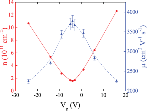
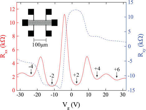
The magnetic field is then set to and the gate voltage is scanned once more at . Multiple quantum Hall levels for monolayer graphene were seen, as shown in Fig. 4. Clear plateaux for the Hall resistance, , at filling factors of and Landau level index are seen with corresponding drops in the longitudinal resistance, . Zhang et al. (2005) Further magnetoresistance measurements were performed to find charge carrier density and mobility at nine different gate voltages with the result shown in Fig. 5. At the CNP, the mobility is measured to be around and the charge carrier density is . These measurements show that the fabrication method presented here results in a mobility at the charge neutral point that approaches values obtained when using exfoliated graphene on SiO2, Huang et al. (2015) implying that the graphene is very clean and has been minimally damaged by the sample production process.
In summary, we have presented a procedure that results in clean large-area graphene devices of high quality on a SiO2 substrate. The 2-step liftoff aids greatly in unbroken large graphene structures, and the 2-step annealing process as well as other cleaning steps result in a realization of near-ideal mobilities and a low hysteresis with observation of quantum Hall levels. Hence, our processing approach now enables large-scale integration of high-quality graphene layers in devices such as THz-emitters, thermo-power couplers, and possibly flexible thin-film sensors.
The authors acknowledge funding support by the MURI’08 of the Air Force Office of Scientific Research (AFOSR, Award No. FA9550-08-1-0337), and the Center for Ultrafast Imaging (CUI) at the University of Hamburg, which is sponsored by the Deutsche Forschungsgemeinschaft (DFG) through grant EXC-1074.
References
- Neto et al. (2009) A. C. Neto, F. Guinea, N. Peres, K. S. Novoselov, and A. K. Geim, “The electronic properties of graphene,” Rev. Mod. Phys. 81, 109 (2009).
- Bolotin et al. (2008) K. I. Bolotin, K. Sikes, Z. Jiang, M. Klima, G. Fudenberg, J. Hone, P. Kim, and H. Stormer, “Ultrahigh electron mobility in suspended graphene,” Solid State Commun. 146, 351–355 (2008).
- Du et al. (2008) X. Du, I. Skachko, A. Barker, and E. Y. Andrei, “Approaching ballistic transport in suspended graphene,” Nat. Nanotechnol. 3, 491–495 (2008).
- Dean et al. (2010) C. R. Dean, A. F. Young, I. Meric, C. Lee, L. Wang, S. Sorgenfrei, K. Watanabe, T. Taniguchi, P. Kim, K. Shepard, et al., “Boron nitride substrates for high-quality graphene electronics,” Nat. Nanotechnol. 5, 722–726 (2010).
- Banszerus et al. (2015) L. Banszerus, M. Schmitz, S. Engels, J. Dauber, M. Oellers, F. Haupt, K. Watanabe, T. Taniguchi, B. Beschoten, and C. Stampfer, “Ultrahigh-mobility graphene devices from chemical vapor deposition on reusable copper,” Sci. Adv. 1, e1500222 (2015).
- Petrone et al. (2012) N. Petrone, C. R. Dean, I. Meric, A. M. van Der Zande, P. Y. Huang, L. Wang, D. Muller, K. L. Shepard, and J. Hone, “Chemical vapor deposition-derived graphene with electrical performance of exfoliated graphene,” Nano Lett. 12, 2751–2756 (2012).
- Yan et al. (2012) Z. Yan, J. Lin, Z. Peng, Z. Sun, Y. Zhu, L. Li, C. Xiang, E. L. Samuel, C. Kittrell, and J. M. Tour, “Toward the synthesis of wafer-scale single-crystal graphene on copper foils,” ACS Nano 6, 9110–9117 (2012).
- Bunch et al. (2007) J. S. Bunch, A. M. Van Der Zande, S. S. Verbridge, I. W. Frank, D. M. Tanenbaum, J. M. Parpia, H. G. Craighead, and P. L. McEuen, “Electromechanical resonators from graphene sheets,” Science 315, 490–493 (2007).
- Zang et al. (2015) X. Zang, Q. Zhou, J. Chang, Y. Liu, and L. Lin, “Graphene and carbon nanotube (cnt) in mems/nems applications,” Microelectron. Eng. 132, 192–206 (2015).
- Liang et al. (2011) X. Liang, B. A. Sperling, I. Calizo, G. Cheng, C. A. Hacker, Q. Zhang, Y. Obeng, K. Yan, H. Peng, Q. Li, et al., “Toward clean and crackless transfer of graphene,” ACS Nano 5, 9144–9153 (2011).
- Suk et al. (2011) J. W. Suk, A. Kitt, C. W. Magnuson, Y. Hao, S. Ahmed, J. An, A. K. Swan, B. B. Goldberg, and R. S. Ruoff, “Transfer of cvd-grown monolayer graphene onto arbitrary substrates,” ACS Nano 5, 6916–6924 (2011).
- Song et al. (2013) J. Song, F.-Y. Kam, R.-Q. Png, W.-L. Seah, J.-M. Zhuo, G.-K. Lim, P. K. Ho, and L.-L. Chua, “A general method for transferring graphene onto soft surfaces,” Nat. Nanotechnol. 8, 356–362 (2013).
- Pimenta et al. (2014) L. G. Pimenta, Y. Song, T. Zeng, M. Dresselhaus, J. Kong, and P. Araujo, “Direct transfer of graphene onto flexible substrates,” in APS Meeting Abstracts, Vol. 1 (2014) p. 37009.
- Her, Beams, and Novotny (2013) M. Her, R. Beams, and L. Novotny, “Graphene transfer with reduced residue,” Phys. Lett. A 377, 1455–1458 (2013).
- Sun et al. (2014) J. Sun, Y. Nam, N. Lindvall, M. T. Cole, K. B. Teo, Y. W. Park, and A. Yurgens, “Growth mechanism of graphene on platinum: Surface catalysis and carbon segregation,” Appl. Phys. Lett. 104, 152107 (2014).
- Liu et al. (2011) M. Liu, X. Yin, E. Ulin-Avila, B. Geng, T. Zentgraf, L. Ju, F. Wang, and X. Zhang, “A graphene-based broadband optical modulator,” Nature 474, 64–67 (2011).
- Tantiwanichapan et al. (2013) K. Tantiwanichapan, J. DiMaria, S. N. Melo, and R. Paiella, “Graphene electronics for terahertz electron-beam radiation,” Nanotechnology 24, 375205 (2013).
- Li et al. (2013) W. Li, Y. Liang, D. Yu, L. Peng, K. P. Pernstich, T. Shen, A. H. Walker, G. Cheng, C. A. Hacker, C. A. Richter, et al., “Ultraviolet/ozone treatment to reduce metal-graphene contact resistance,” Appl. Phys. Lett. 102, 183110 (2013).
- Lee et al. (2013) J. Lee, Y. Kim, H.-J. Shin, C. Lee, D. Lee, C.-Y. Moon, J. Lim, and S. C. Jun, “Clean transfer of graphene and its effect on contact resistance,” Appl. Phys. Lett. 103, 103104 (2013).
- Moser, Barreiro, and Bachtold (2007) J. Moser, A. Barreiro, and A. Bachtold, “Current-induced cleaning of graphene,” Appl. Phys. Lett. 91, 163513 (2007).
- Barreiro et al. (2013) A. Barreiro, F. Börrnert, S. M. Avdoshenko, B. Rellinghaus, G. Cuniberti, M. H. Rümmeli, and L. M. Vandersypen, “Understanding the catalyst-free transformation of amorphous carbon into graphene by current-induced annealing,” Sci. Rep. 3 (2013).
- Goossens et al. (2012) A. Goossens, V. Calado, A. Barreiro, K. Watanabe, T. Taniguchi, and L. Vandersypen, “Mechanical cleaning of graphene,” Appl. Phys. Lett. 100, 073110 (2012).
- Chen et al. (2012) C. W. Chen, F. Ren, G.-C. Chi, S.-C. Hung, Y. Huang, J. Kim, I. I. Kravchenko, and S. J. Pearton, “Uv ozone treatment for improving contact resistance on graphene,” J. Vac. Sci. Technol. B 30, 060604 (2012).
- Pirkle et al. (2011) A. Pirkle, J. Chan, A. Venugopal, D. Hinojos, C. Magnuson, S. McDonnell, L. Colombo, E. Vogel, R. Ruoff, and R. Wallace, “The effect of chemical residues on the physical and electrical properties of chemical vapor deposited graphene transferred to sio2,” Appl. Phys. Lett. 99, 122108 (2011).
- Ishigami et al. (2007) M. Ishigami, J. Chen, W. Cullen, M. Fuhrer, and E. Williams, “Atomic structure of graphene on sio2,” Nano Lett. 7, 1643–1648 (2007).
- Nagashio et al. (2011) K. Nagashio, T. Yamashita, T. Nishimura, K. Kita, and A. Toriumi, “Electrical transport properties of graphene on sio2 with specific surface structures,” J. Appl. Phys. 110, 024513 (2011).
- Nath et al. (2014) A. Nath, A. D. Koehler, G. G. Jernigan, V. D. Wheeler, J. K. Hite, S. C. Hernández, Z. R. Robinson, N. Y. Garces, R. L. Myers-Ward, C. R. Eddy Jr, et al., “Achieving clean epitaxial graphene surfaces suitable for device applications by improved lithographic process,” Appl. Phys. Lett. 104, 224102 (2014).
- Ferrari et al. (2006) A. Ferrari, J. Meyer, V. Scardaci, C. Casiraghi, M. Lazzeri, F. Mauri, S. Piscanec, D. Jiang, K. Novoselov, S. Roth, et al., “Raman spectrum of graphene and graphene layers,” Phys. Rev. Lett. 97, 187401 (2006).
- Adam et al. (2007) S. Adam, E. Hwang, V. Galitski, and S. D. Sarma, “A self-consistent theory for graphene transport,” P. Natl. Acad. Sci. USA 104, 18392–18397 (2007).
- Novoselov et al. (2004) K. S. Novoselov, A. K. Geim, S. V. Morozov, D. Jiang, Y. Zhang, S. V. Dubonos, I. V. Grigorieva, and A. A. Firsov, “Electric field effect in atomically thin carbon films,” Science 306, 666–669 (2004).
- Giovannetti et al. (2008) G. Giovannetti, P. Khomyakov, G. Brocks, V. v. Karpan, J. Van den Brink, and P. Kelly, “Doping graphene with metal contacts,” Phys. Rev. Lett. 101, 026803 (2008).
- Nagashio and Toriumi (2011) K. Nagashio and A. Toriumi, “Density-of-states limited contact resistance in graphene field-effect transistors,” Jpn. J. Appl. Phys. 50, 070108 (2011).
- Lafkioti et al. (2010) M. Lafkioti, B. Krauss, T. Lohmann, U. Zschieschang, H. Klauk, K. v. Klitzing, and J. H. Smet, “Graphene on a hydrophobic substrate: doping reduction and hysteresis suppression under ambient conditions,” Nano Lett. 10, 1149–1153 (2010).
- Fang et al. (2007) T. Fang, A. Konar, H. Xing, and D. Jena, “Carrier statistics and quantum capacitance of graphene sheets and ribbons,” Appl. Phys. Lett. 91, 092109 (2007).
- Zhang et al. (2005) Y. Zhang, Y.-W. Tan, H. L. Stormer, and P. Kim, “Experimental observation of the quantum hall effect and berry’s phase in graphene,” Nature 438, 201–204 (2005).
- Huang et al. (2015) Y. Huang, E. Sutter, N. N. Shi, J. Zheng, T. Yang, D. Englund, H.-J. Gao, and P. Sutter, “Reliable exfoliation of large-area high-quality flakes of graphene and other two-dimensional materials,” ACS Nano 9, 10612–10620 (2015).