Surface vibrational modes of the topological insulator Bi2Se3 observed by Raman spectroscopy
Abstract
We present polarization resolved Raman scattering study of surface vibration modes in the topological insulator Bi2Se3 single crystal and thick films. Besides the four Raman active bulk phonons, we observed four additional modes with much weaker intensity and slightly lower energy than the bulk counterparts. Using symmetry analysis, we assigned these additional modes to out-of-plane surface phonons. Comparing with first principle calculations, we conclude that the appearance of these modes is due to -axis lattice distortion and van der Waals gap expansion near the crystal surface. Two of the surface modes at 60 and 173 cm-1 are associated with Raman active bulk phonon modes, the other two at 136 and 158 cm-1 are associated with infrared active bulk phonons with symmetry. The latter become Raman allowed due to reduction of crystalline symmetry from in the bulk to on the crystal surface. In particular, the 158 cm-1 surface phonon mode shows a Fano lineshape under resonant excitation, suggesting interference in the presence of electron-phonon coupling of the surface excitations.
I Introduction
| Sample # | Composition | Description | Growth |
|---|---|---|---|
| #2 | Bi2Se3 | 50 QL thick film | MBE |
| #8 | (Bi2Se3)m(In2Se3)n | 50 nm superlattice with (m,n)=(5,5) | MBE |
| #10 | (Bi2Se3)m(In2Se3)n | 50 nm superlattice with (m,n)=(10,5) | MBE |
| #13 | Bi1.95In0.05Se3 | single crystal with indium doping | Bridgman |
| #14 | Bi2Se3 | pristine single crystal | Bridgman |
| #A | Bi2Se3 | pristine single crystal | Bridgman |
Topological insulators (TIs) are a new class of quantum matter characterized by linearly dispersed spin polarized gapless surface states within the bulk band gaps Fu et al. (2007); Zhang et al. (2009); Hsieh et al. (2009); Xia et al. (2009); Checkelsky et al. (2009); Bianchi et al. (2010); Beidenkopf et al. (2011); Hasan and Moore (2011), which may lead to realization of novel phenomena and applications such as spintronics and quantum computing Fu and Kane (2008); Qi et al. (2008, 2009); Hasan and Kane (2010); Yu et al. (2010); Raghu et al. (2010); Hasan and Moore (2011); Qi and Zhang (2011); Wang et al. (2013); Grover et al. (2014).
Despite the topological protection, the surface states away from the Dirac point suffer from hexagonal warping effect, resulting in increased scattering rate at the TI surface Butch et al. (2010); Pan et al. (2012); Valla et al. (2012). Among many possible inelastic scattering mechanisms, electron-phonon interaction is especially important due to its direct impact on device applications at finite temperature Parente et al. (2013); Costache et al. (2014). In particular, the self-energies and symmetries of the surface vibrational modes are essential for modeling the possible relaxation channels of the surface state excitations.
Theoretical modeling of surface lattice dynamics was first developed by Lifshitz and Rosenzweig Lifshitz and Rosenzweig (1948); Lifshitz (1956), and later expanded by various workers Wallis (1957, 1959); Benedek and Miglio (1991); Wallis (1994). The basic idea is to consider the free surface as a perturbation of an infinite lattice, and therefore to derive the surface modes from the spectrum of bulk vibrations. As a result, the frequencies of atomic vibration modes at the surface are modified to a smaller value than in the bulk at the Brillouin zone center ( point). If there is a gap in the phonon density-of-state (DOS) and with large enough distortion, the surface phonon DOS can be entirely separated from the bulk Lifshitz and Rosenzweig (1948); Wallis (1959). Such modes are long lived and localized at the surface, where the dispersion can be quite different than the bulk Lagos et al. (2017). However, it is often experimentally challenging to distinguish surface signal from the overwhelmingly stronger intensity contribution of the bulk. Moreover, if the surface vibration mode is not completely gapped out from the bulk spectrum, then the surface and bulk modes are indistinguishable. Instead, the “bulk phonon” acquires only a slight energy shift near the crystal surface. Notice that the surface modes originate from abrupt termination of the lattice restoring force across bulk/vacuum interface in a semi-infinite crystal, and should not be confused with the phonons in quasi-2D ultrathin samples, which are almost decoupled from the underlying substrate of a different material Zhao et al. (2011); Zhang et al. (2011); Chis et al. (2012); Humlíček et al. (2014); Eddrief et al. (2014).
Bi2Se3 is one of the most studied TI due to its relatively simply band structure, i.e., a single Dirac cone within the 0.3 eV bulk band gap, much larger than the thermal energy at the room temperature. While the bulk phonon modes have been extensively studied in Bi2Se3 single crystals Köhler and Becker (1974); Richter and Becker (1977); LaForge et al. (2010); Zhao et al. (2011); Zhang et al. (2011); Gnezdilov et al. (2011); Kim et al. (2012); Humlíček et al. (2014); Irfan et al. (2014); Eddrief et al. (2014); Yan et al. (2015); Zhang et al. (2016), only a few papers have reported studies of the surface vibration modes. Zhu and coworkers observed strong Kohn anomaly at about using helium atom scattering (HAS) Zhu et al. (2011), and deduced the interaction between surface phonon and the Dirac electrons to be much stronger than the values previously reported by angle-resolved photoemission spectroscopy (ARPES) measurements Zhu et al. (2012); Howard et al. (2013); Hatch et al. (2011); Pan et al. (2012), suggesting that the electron-phonon coupling on TI surface may be more complex than anticipated. Time-resolved ARPES study of single crystals reported the observation of one bulk phonon at about 74 cm-1, and an additional mode with slightly lower energy consistent with what was suggested by transport measurements Costache et al. (2014). This mode was interpreted as a surface phonon associated with the observed bulk phonon Sobota et al. (2014). However, alternative results have also been reported Hatch et al. (2011); Pan et al. (2012); Chen et al. (2013); Kondo et al. (2013), suggesting the existence of multiple phononic decaying channels which may depend on details of sample preparation. Electron energy loss spectroscopy (EELS) study has distinguished a weak mode at about 160 cm-1 in Bi2Se3, which was assigned to the surface vibration mode associated with an bulk phonon Kogar et al. (2015). The Raman scattering work on bulk single crystal Gnezdilov et al. (2011) and exfoliated nano-crystals reported several additional features, and were attributed to infrared active phonon modes becoming Raman active due to inversion symmetry breaking at crystal surface Eddrief et al. (2014); Zhao et al. (2011).
To date, different surface modes were measured by several distinct spectroscopies, with slight discrepancies between the results and interpretations. To resolve the discrepancy, it is desirable to study all surface vibration modes within one technique that provides both high energy resolution and symmetry information.
Raman spectroscopy is a conventional tool for studying surface phonon modes Esser and Richter (1999); Liebhaber et al. (2014). Here, we use high resolution polarization resolved Raman spectroscopy to study the vibrational modes in Bi2Se3 samples. We focus our study to the bulk single crystals, which are unexposed to air or any chemicals. In addition to the four Raman active bulk phonons, we observed 6 additional modes with about 20–100 times weaker intensities compared to the bulk phonons [Fig. 1]. By comparing the data to the results obtained by the complementary spectroscopic techniques and the calculations, we assign the observed additional modes to surface phonons arising from out-of-plane lattice distortion near the crystal/film interface.
This paper is organized as follows. In Sec. II, we introduce the experiments including sample preparations and the Raman probe. In Sec. III, we present the low temperature polarized Raman spectra of bulk and thin film Bi2Se3 samples. Sec. IV discusses the symmetries and microscopic views of the surface vibration modes. Finally, we conclude our discussions in Sec. V. Details of data analysis are given in Appendix.
II Experimental setup
Table 1 lists 6 Bi2Se3 single crystals and films measured in this study. The bulk single crystals were grown by modified Bridgman method LošŤák et al. (1990); Dai et al. (2016). The thin film samples were epitaxially grown on Al2O3 (0001) substrates in a custom designed molecular beam epitaxy (MBE) chamber Brahlek et al. (2012); Bansal et al. (2012). They were immediately transfered into a cryostat after taking out of MBE chamber.
The superlattice thin films of (Bi2Se3)m(In2Se3)n are grown along (0001) surface Brahlek et al. (2012), where each primitive cell consists of quintuple layer (QL) Bi2Se3 and QL In2Se3, with each QL being nm thick. Notice that the light penetration depth in Bi2Se3 within energy range of current study is about 10 nm J. W. et al. (2012). Therefore, the signal is dominated by scattering from the first few QLs of Bi2Se3, and the scattering volume in the superlattice samples is practically the same as bulk.
Bi2Se3 has a rhombohedral crystal structure with the point group symmetry. The irreducible representations and Raman selection rules are given in Table 2. With five atoms in a primitive unit cell, there are a total of three acoustic and 12 optical bulk phonon branches. At the -point, the irreducible representations of the Raman active phonons are , and the infrared active phonons are Köhler and Becker (1974); Richter and Becker (1977). These bulk phonon modes have been measured by Raman and infrared spectroscopies Köhler and Becker (1974); Richter and Becker (1977); LaForge et al. (2010); Zhao et al. (2011); Zhang et al. (2011); Gnezdilov et al. (2011); Kim et al. (2012); Humlíček et al. (2014); Irfan et al. (2014); Eddrief et al. (2014); Yan et al. (2015); Zhang et al. (2016), and the values reported in Ref. LaForge et al. (2010) and Ref. Gnezdilov et al. (2011) are listed in Table 3.
The crystal naturally cleaves along the (111) surface terminated at Se atoms, forming optically flat QLs weakly bonded by van der Waals force Köhler and Becker (1974). The surface QL has the symmorphic wallpaper group symmetry (two dimensional crystallographic point group ) Terzibaschian and Enderlein (1986); Li et al. (2013); Slager et al. (2013). Since the surface layer phonon modes in Bi2Se3 are not perfectly localized and decay into the bulk, it is more appropriate to analyze our experimental results within the layer group (crystallographic point group , which is a subgroup containing common symmetry operators of and groups) Li et al. (2013).
All Raman scattering measurements are taken from ab surfaces freshly cleaved or grown immediately prior to the measurements. Sample #2–14 are measured in a quasi-backscattering geometry in a continuous He-flow optical cryostat. A glove bag with controlled dry nitrogen gas environment was sealed to the cryostat loading port. After purging the bag to the desired conditions, the single crystals were cleaved in the glove bag immediately before loading into the cryostat for cooling, without exposure to air. We use 532 nm solid state laser for excitation, where the spot size is roughly . The scattered light was analyzed and collected by a custom triple-grating spectrometer equipped with a liquid nitrogen cooled CCD detector.
As for the data collected from sample #A, measurements were done in a back-scattering geometry from a cold-finger cryostat. An argon ion laser and a Ti:Sapphire laser were used as sources, where the spot sizes are roughly 35 and 55 , respectively. The scattered light was collected using a triple stage spectrometer (Dilor XY) and imaged on a CCD camera.
All spectra shown were corrected for the spectral response of the spectrometer and CCD to obtain the Raman intensity , which is related to the Raman response function by the Bose factor : . Here, () denotes the polarization of incident (scattered) photon, is energy and is temperature. The scattering geometries used in this experiment are denoted as and , which is short for in Porto’s notation. and denotes the right- and left-circular polarizations, respectively, where X (Y) denotes linear polarization parallel (perpendicular) to the plane of incidence. The irreducible representations of the and groups corresponding to these scattering geometries are listed in Table 2. Notice that in both the and groups, the phonon intensities do not depend on the orientation of the crystallographic axis. The notations and have no reference to the crystallographic a and b axes. In order to avoid confusion with the weak surface modes, possible polarization leakage arising from optical elements are removed from presented data with a procedure described in Appendix.
| Scattering | Bulk | Surface |
|---|---|---|
| geometry | () | () |
| RR | ||
| RL | ||
| XX | ||
| YX |
III Results
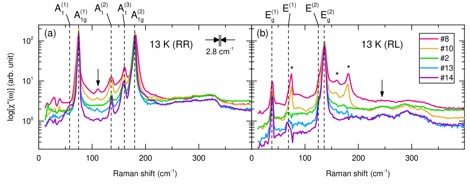
Figure 1 shows the Raman response function , taken at 13 K with 532 nm excitation, plot in semi-log scale. In order to confirm the tiny features of surface modes, we compared the results from bulk crystals and MBE films. Figures 1(a) and 1(b) are measured with the RR and RL scattering geometries, respectively (Table 2). The dashed lines label the observed phonons as tabulated in Table 3. The strong modes at 72 and 174 cm-1 in RR scattering geometry are the bulk phonons of Bi2Se3 [Fig. 1(a)], and the strong modes centered at 37 and 132 cm-1 in RL are the bulk phonons [Fig. 1(b)], consistent with previous Raman studies Zhang et al. (2011); Gnezdilov et al. (2011) and calculations Wang and Zhang (2012).
The broad feature at about 330 cm-1 in RR is possibly due to second-order scattering of the phonon, broadened due to the large downward dispersion of the phonon branch Wang and Zhang (2012). Similarly, the broad feature observed around 300 cm-1 in RL is assigned to two-phonon excitation, . The broad feature at about 245 cm-1 [Fig. 1(b), marked by arrow] was previously assigned to the 2D stretching mode of Se atoms on the surface Glinka et al. (2015). However, we do not observe the reported resonance effect of this mode with near-infrared excitation [Fig. 2]. Notice that this mode energy is also consistent with the two-phonon excitation of .
In order to distinguish the broad features from electronic origin, such as excitations from the topological surface states, we compared the results with indium doped Bi2Se3 in Fig. 1. Indium doping was shown to increase the carrier density and suppress the topological surface states in Bi2Se3 Brahlek et al. (2012); Wu et al. (2013). Here, we collected data from bulk single crystals and MBE grown In2Se3/Bi2Se3 superlattices, where indium doping is achieved through diffusion in the superlattices Lee et al. (2014). In all indium doped samples, the broad features show the same intensity, suggesting their origin unrelated to the topological surface states. This feature is slightly weaker in the superlattice sample #8, despite the first-order phonon modes are still sharp and strong. However, this is likely mainly due to the indium atom diffusion into the Bi2Se3 layer, which breaks the translation symmetry, and therefore further broadens the multi-phonon mode. The diffused indium atoms also lower the local crystal symmetry in the Bi2Se3 layers, and therefore allows vibration modes with and symmetries to appear in the RL geometry, which is otherwise forbidden for the crystal symmetry of Bi2Se3 [Fig. 1(b), marked by asterisks]. The small feature at 110 cm-1 in RR is due to a strong phonon of -In2Se3 layers Lewandowska et al. (2001) (indicated by arrow in Fig. 1(a)).
In addition to the strong bulk first-order Raman phonons and the broad features, we see additional sharp modes that are about 20 times weaker than the bulk phonons. In Fig. 1(a), two such features at 136 and 158 cm-1 are seen in all samples in RR scattering geometry, labeled and , respectively. In the bulk single crystal sample #14, we observed a mode at about 60 cm-1, which we label as . We associate these three features with vibration modes at the crystal surface, to be discussed in the RR polarization for the Sample #14 in the next section. We also noticed several sharp features below 50 cm-1 in sample #8 and #10 in RR, which are possibly zone folded phonons. To confirm this requires further studies, and is beyond the scope of this paper. In the RL scattering geometry, we observed two weak features at 67 and 126 cm-1, labeled and , respectively [Fig. 1(b)]. The energy of these modes are close to the strong bulk phonons, and therefore require higher resolution to distinguish them.
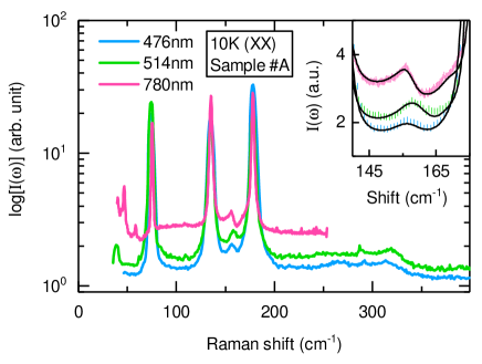
In Fig. 2 are the Raman spectra of the bulk sample at different excitation wavelengths at 10 K. The spectra were obtained in the XX polarization. As in Fig. 1, we observe an additional peak at 158 cm-1 which we refer to as . However, note that the mode is more asymmetric when 780 nm excitation wavelength is used. This is an indication that the phonon is interacting with a continuum.
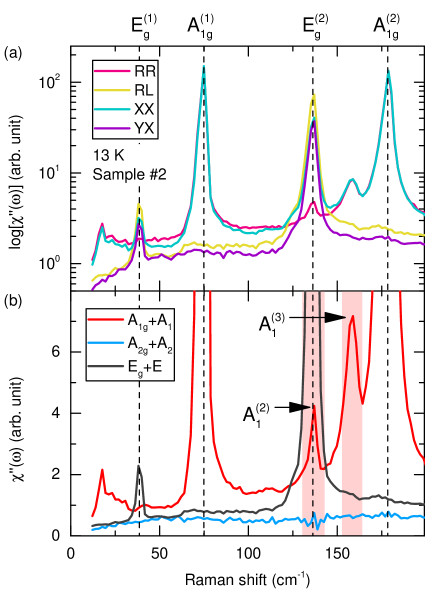
To further understand the observed phonon modes, we measure the Raman response in four scattering geometries of the and point group as listed in Table 2 [Fig. 3(a)]. The intensity contributed by each symmetry channel in different scattering geometries are dictated by the Raman tensors Cardona (1982); Ovander (1960) and the results for and groups are listed in Table 2. Therefore, by obtaining polarized Raman spectra in four proper scattering geometries, we can separate the measured Raman response from each symmetry channel.
| (1) | |||||
The results are shown in Fig. 3(b). We notice that no lattice vibrational mode is observed in the and symmetry channels. This is because the Raman tensors for these two channels are antisymmetric and commonly correspond to pseudo-vector-like excitations Ovander (1960); Shastry and Shraiman (1991); Khveshchenko and Wiegmann (1994), which is forbidden for phononic Raman scattering in Bi2Se3. Since the signal in and channels are expected to be zero, we can claim that all vibration modes appearing in RR have either or symmetry (Table 2).
The mode happens to have energy very close to the phonon, making it particularly difficult for spectroscopic experiments to distinguish. Here, we utilize the symmetry properties to separately detect them with polarized light. The polarization leakage of optical elements are precisely measured and removed (Appendix), and thereby excluding the possibility of being a trivial polarization leakage from the phonon.
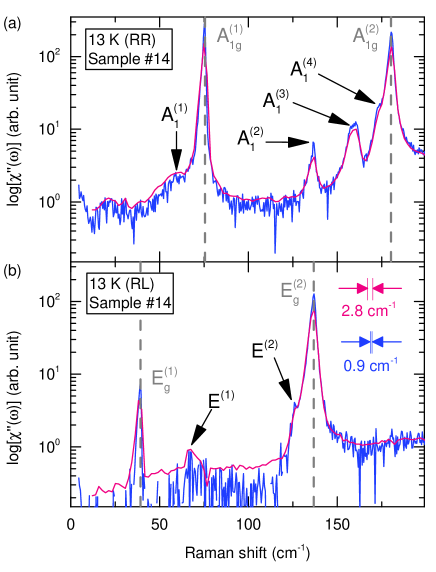
To distinguish surface modes that are particularly weak and close in energy to the bulk phonons, we take high resolution spectra from a carefully prepared bulk crystal #14, cleaved in nitrogen environment. We show in Fig. 4 the spectra taken at 13 K in RR and RL scattering geometries, where the smoother low resolution (2.8 cm-1) data is overlapped with the high resolution (0.9 cm-1) spectra. Besides the more pronounced and modes already visible in Fig. 3, we see a few additional features in the high resolution data: (1) A mode centered at 173 cm-1 appearing as a shoulder to the bulk phonon in RR geometry [Fig. 4(a)], which we designate as . (2) Another mode centered at 126 cm-1 appearing as a shoulder to the bulk phonon in RL geometry [Fig. 4(b)], which we designate as . (3) The mode shows broadened peak structure. This cannot be due to splitting of an -symmetry phonon, e.g., lowering of symmetry, since is a one-dimensional representation. This can be explained as due to Fano interference, which become more pronounced with infrared excitation [Fig. 2].
IV Discussion
| Experiment | Calculation | ||||
|---|---|---|---|---|---|
| Symmetry | This work | Literature | LDA+SOI Wang and Zhang (2012) | GGA+SOI Cheng and Ren (2011) | |
| 75 | 73 Gnezdilov et al. (2011); Zhang et al. (2011); Irfan et al. (2014); Zhang et al. (2016) | 77 | 64 | ||
| 180 | 175 Gnezdilov et al. (2011); Zhang et al. (2011); Irfan et al. (2014); Zhang et al. (2016) | 176 | 167 | ||
| 39 | 39 Gnezdilov et al. (2011); Zhang et al. (2011); Irfan et al. (2014); Zhang et al. (2016) | 41 | 39 | ||
| 137 | 133 Gnezdilov et al. (2011); Zhang et al. (2011); Irfan et al. (2014); Zhang et al. (2016) | 139 | 124 | ||
| – | N/A | 139 | 137 | ||
| – | N/A | 161 | 156 | ||
| – | 61 LaForge et al. (2010) | 80 | 65 | ||
| – | 133 LaForge et al. (2010) | 131 | 127 | ||
| 60 | 68 Sobota et al. (2014) | N/A | N/A | ||
| 136 | 129 Gnezdilov et al. (2011) | N/A | N/A | ||
| 158 | 160 Gnezdilov et al. (2011); Kogar et al. (2015) | N/A | N/A | ||
| 173 | N/A | N/A | N/A | ||
| 67 | 68 Gnezdilov et al. (2011) | N/A | N/A | ||
| 126 | 125 Gnezdilov et al. (2011) | N/A | N/A | ||
At the crystal surface of Bi2Se3, the lattice structure is distorted along c-axis due to the abrupt reduction of the interlayer van der Waals force that binds the crystal together, and is calculated by density functional theory (DFT) to be about 10% along -axis Sobota et al. (2014). Additionally, the observation of two-dimensional electron gas formed on Bi2Se3 surface also supports the picture of subsurface van der Waals gap expansion Bianchi et al. (2010, 2012); Menshchikova et al. (2011). However, finite phonon DOS exist across the entire energy range in Bi2Se3 Wang and Zhang (2012), allowing the surface modes to decay into bulk phonon modes. Therefore, the surface mode is not entirely “peeled off” from the bulk. Instead, one would expect a “surface resonance” with slightly lower energy than the bulk phonon.
Due to inversion symmetry breaking at the crystal interface, the surface resonance from the Raman active and IR active phonons are both expected to appear in the symmetry ( group), corresponding to out-of-plane atomic motion. The energies of such surface modes are usually slightly lower than the corresponding bulk phonons. This is consistent with the four modes we observed [Fig. 4(a)]. From the energies of these modes, we conclude that and are associated with the bulk phonon modes and , respectively. The measured energy of the mode is somewhat different than the previously reported value of 68 cm-1 by time resolved ARPES Sobota et al. (2014), but close to what was suggested by transport measurements Costache et al. (2014). We believe this difference may be partly due to surface quality variation. ARPES measured sample is usually cleaved in ultra high vacuum, whereas the surface in this study is cleaved in nitrogen environment. This may also explain why this mode was not observed in the MBE samples [Fig. 1], where the sample is unavoidably exposed to air for a few minutes during the transfer between MBE chamber and Raman cryostat. The mode appears as a shoulder to the bulk phonon, requiring higher resolution to distinguish from the bulk mode, and therefore was overlooked in the previous Raman study Gnezdilov et al. (2011).
In comparison, the surface modes and have higher intensity and are better resolved. One possibility for this difference is that the bulk counterpart of these modes are the IR active and phonons, as the measured energy is close to the calculated values (Table 3). Since these bulk modes are not Raman active, we were able to better resolve the surface resonance. Another possibility is that the phonon DOS is practically zero at these energies in the symmetry channel, and the surface vibration modes are truly localized. Distinguishing these two scenarios is in fact experimentally non-trivial, especially since the experimental values of the and bulk phonon energies are yet unknown.
Nevertheless, both possibilities point to the surface origin of these two modes, which provide us with information on the electron-phonon coupling at the TI surface. While the bulk phonons show little resonance effect, the phonon displays antisymmetric lineshape with 780 nm excitation, reminiscent of a Fano lineshape Fano (1961) [Fig. 2, inset]. This was overlooked in previous Raman studies, and may be related to the 20 meV “kink” in the topological surface state’s energy dispersion curve reported by some ARPES measurements Kondo et al. (2013); Chen et al. (2013). The observation of Fano lineshape is a clear evidence for the existence of underlying electronic continuum in the symmetry channel, which interacts with the phonon Fano (1961); Klein (1983). The excitation dependence also suggests resonance enhancement of the electronic continuum with near-infrared wavelength, consistent with the reported surface states at about 1.6 eV above the Fermi energy Sobota et al. (2013); Niesner et al. (2012). Fitting the 780 nm data with Eq. 4.48 in Ref. Klein (1983):
| (2) |
yields electron-phonon interaction strength cm-1, and phonon energy cm-1. Here we assumed the electron DOS is a constant in the relevant energy window, and neglect the real part of the electronic Green’s function . and are the phonon and electronic continuum Raman transition matrix elements, respectively.
Since the in-plane symmetries are mainly preserved as the DFT calculated atomic surface distortion is purely out-of-plane Sobota et al. (2014), one would not expect surface phonon with symmetry ( group) for Bi2Se3. However, the in-plane bonding potential is also modified by having distortion along c-axis, and therefore the phonon frequency at surface is still slightly different than the bulk value. If the modification is tiny, the modes are expected to be weak and close to the bulk phonons. In Fig. 1(b) and Fig. 4(b), we can see hints of two additional modes, labeled by and . The energies of these modes are in fact close to the measured values of and bulk phonons Richter and Becker (1977); LaForge et al. (2010), and are consistent with the previous Raman study Gnezdilov et al. (2011) (Table 3). However, the frequency of is slightly higher than , which is against the expectation from a surface resonance. This may reflect the fact that this is an in-plane mode, orthogonal to the lattice distortion direction. Or, this may be indicative of non-trivial electron-phonon interaction with the surface states, and worth further studying.
V Conclusion
In conclusion, we have done systematic symmetry analysis on the temperature and excitation dependent Raman spectra from high quality, freshly cleaved or grown ab surfaces of Bi2Se3 single crystal and films. We observed in total four out-of-plane, and possibly 2 in-plane surface vibrational modes, where we tabulate the energies and symmetries in Table 3.
In particular, we reproduced the mode, which was previously observed in time resolved ARPES measurements Sobota et al. (2014). The mode is interesting because it was found to couple strongly with the topological surface states, and therefore provides the main phononic decay channel for the Dirac fermions in Bi2Se3. Our report of energies and symmetries of the and other surface modes affirms the validity of the surface lattice distortion model employed in Ref. Sobota et al. (2014). The consistently much larger intensity for the out-of-plane vibration modes compared to in-plane modes strongly suggest that the surface lattice distortion and van der Waals gap expansion in Bi2Se3 is only along -axis.
Lastly, the and modes have much stronger intensities compared to the other surface vibration modes, and may be candidates for localized surface phonons. In particular, we noticed the mode possesses a Fano lineshape in low doped Bi2Se3 single crystals. The Fano lineshape is indicative of electron-phonon coupling with the underlying electronic continuum of the same symmetry, important for understanding the relaxation and scattering of surface state excitations. Here, we found a resonance effect to the Fano lineshape with 780 nm excitation, suggesting the onset of the electronic continuum in symmetry has excitation dependence. This explains the inconsistent surface electron-phonon coupling constant found in previous ARPES studies Pan et al. (2012); Hatch et al. (2011). The excitation dependence also confirms the existence of unoccupied surface states at about 1.6 eV above the Fermi energy, which enhances the surface electronic continuum through resonance effect.
Acknowledgements.
G.B. and H.-H.K acknowledge support from the U.S. DOE, BES grant DE-SC0005463 for spectroscopic studies. S.O., M.S., N.K. and M.B. acknowledge support by Gordon and Betty Moore Foundation’s EPiQS initiative (GBMF4418) and NSF(EFMA-1542798) for film growth. S.-W.C. and X.W. acknowledge support from NSF Award DMREF-1233349 for single crystal growth. G.B. also acknowledges partial support from QuantEmX grant from ICAM and the Gordon and Betty Moore Foundation through Grant GBMF5305 and from the European Regional Development Fund project TK134.*
Appendix A Removal of polarization leakage
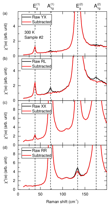
In this section, we explain the details of data analysis concerning removal of polarization leakage from optical elements. The degree of leakage are determined from the and bulk phonons of single crystal samples at room temperature. The removal of polarization leakage is done by subtracting intensity from the orthogonal polarization geometry, i.e., , where and are raw data taken in YX and XX polarization geometries, respectively, and is the leakage ratio due to the limitations of polarization optics. It is reasonable to suggest that the same ratio also applies to XX polarization geometry: . Similarly, we have and for the circularly polarized geometries, where is the leakage ratio due to the limitations of the broadband quarter wave plate and alignment of the Berek compensator. The ratios and are in general a weak function of , but in a narrow energy window as in this study, they can be safely assumed as constants. In order to avoid confusion from contributions of surface phonons, we chose YX and RL geometries as our reference for determination of and . In these two geometries, only and bulk phonons are expected to be present, the symmetry surface modes are extremely weak and close to the bulk phonons [Fig. 4], and therefore do not raise concern for determination of and .
In Fig. 5, we show spectra of unprocessed raw data and polarization leakage removed results taken at 300 K from the ab surface of a Bi2Se3 thick film in black and red lines, respectively. The leakage intensity of and bulk phonons in raw data taken with YX and RL geometries can be fully removed with leakage ratios and , respectively. These values are within the specification of used broadband polarization optics.
The value of depends only on the wavelength of light, and therefore the same value is used for all samples and temperatures measured with 532 nm excitation. The value of depends critically on the alignment of the Berek compensator, which may vary between experiments, and has to be determined using the method described above in each experiment. In this study, the value of is always within the range .
References
- Fu et al. (2007) Liang Fu, C. L. Kane, and E. J. Mele, “Topological insulators in three dimensions,” Phys. Rev. Lett. 98, 106803 (2007).
- Zhang et al. (2009) Haijun Zhang, Chao-Xing Liu, Xiao-Liang Qi, Xi Dai, Zhong Fang, and Shou-Cheng Zhang, “Topological insulators in Bi2Se3, Bi2Te3 and Sb2Te3 with a single Dirac cone on the surface,” Nature Phys. 5, 438 (2009).
- Hsieh et al. (2009) D. Hsieh, Y. Xia, D. Qian, L. Wray, J. H. Dil, F. Meier, J. Osterwalder, L. Patthey, J. G. Checkelsky, N. P. Ong, A. V. Fedorov, H. Lin, A. Bansil, D. Grauer, Y. S. Hor, R. J. Cava, and M. Z. Hasan, “A tunable topological insulator in the spin helical Dirac transport regime,” Nature 460, 1101–1105 (2009).
- Xia et al. (2009) Y. Xia, D. Qian, D. Hsieh, L. Wray, A. Pal, H. Lin, A. Bansil, D. Grauer, Y. S. Hor, R. J. Cava, and M. Z. Hasan, “Observation of a large-gap topological-insulator class with a single Dirac cone on the surface,” Nature Phys. 5, 398–402 (2009).
- Checkelsky et al. (2009) J. G. Checkelsky, Y. S. Hor, M.-H. Liu, D.-X. Qu, R. J. Cava, and N. P. Ong, “Quantum interference in macroscopic crystals of nonmetallic Bi2Se3,” Phys. Rev. Lett. 103, 246601 (2009).
- Bianchi et al. (2010) Marco Bianchi, Dandan Guan, Shining Bao, Jianli Mi, Bo Brummerstedt Iversen, Philip D. C. King, and Philip Hofmann, “Coexistence of the topological state and a two-dimensional electron gas on the surface of Bi2Se3,” Nat. Commun. 1, 128 (2010).
- Beidenkopf et al. (2011) Haim Beidenkopf, Pedram Roushan, Jungpil Seo, Lindsay Gorman, Ilya Drozdov, Yew San Hor, R. J. Cava, and Ali Yazdani, “Spatial fluctuations of helical Dirac fermions on the surface of topological insulators,” Nature Phys. 7, 939–943 (2011).
- Hasan and Moore (2011) M. Zahid Hasan and Joel E. Moore, “Three-dimensional topological insulators,” Annual Review of Condensed Matter Physics 2, 55–78 (2011).
- Fu and Kane (2008) Liang Fu and C. L. Kane, “Superconducting proximity effect and majorana fermions at the surface of a topological insulator,” Phys. Rev. Lett. 100, 096407 (2008).
- Qi et al. (2008) Xiao-Liang Qi, Taylor L. Hughes, and Shou-Cheng Zhang, “Topological field theory of time-reversal invariant insulators,” Phys. Rev. B 78, 195424 (2008).
- Qi et al. (2009) Xiao-Liang Qi, Rundong Li, Jiadong Zang, and Shou-Cheng Zhang, “Inducing a magnetic monopole with topological surface states,” Science 323, 1184–1187 (2009).
- Hasan and Kane (2010) M. Z. Hasan and C. L. Kane, “Colloquium : Topological insulators,” Rev. Mod. Phys. 82, 3045–3067 (2010).
- Yu et al. (2010) Rui Yu, Wei Zhang, Hai-Jun Zhang, Shou-Cheng Zhang, Xi Dai, and Zhong Fang, “Quantized anomalous hall effect in magnetic topological insulators,” Science 329, 61–64 (2010).
- Raghu et al. (2010) S. Raghu, Suk Bum Chung, Xiao-Liang Qi, and Shou-Cheng Zhang, “Collective modes of a helical liquid,” Phys. Rev. Lett. 104, 116401 (2010).
- Qi and Zhang (2011) Xiao-Liang Qi and Shou-Cheng Zhang, “Topological insulators and superconductors,” Rev. Mod. Phys. 83, 1057–1110 (2011).
- Wang et al. (2013) Y. H. Wang, H. Steinberg, P. Jarillo-Herrero, and N. Gedik, “Observation of Floquet-Bloch states on the surface of a topological insulator,” Science 342, 453–457 (2013).
- Grover et al. (2014) Tarun Grover, D. N. Sheng, and Ashvin Vishwanath, “Emergent space-time supersymmetry at the boundary of a topological phase,” Science 344, 280–283 (2014).
- Butch et al. (2010) N. P. Butch, K. Kirshenbaum, P. Syers, A. B. Sushkov, G. S. Jenkins, H. D. Drew, and J. Paglione, “Strong surface scattering in ultrahigh-mobility Bi2Se3 topological insulator crystals,” Phys. Rev. B 81, 241301 (2010).
- Pan et al. (2012) Z.-H. Pan, A. V. Fedorov, D. Gardner, Y. S. Lee, S. Chu, and T. Valla, “Measurement of an exceptionally weak electron-phonon coupling on the surface of the topological insulator Bi2Se3 using angle-resolved photoemission spectroscopy,” Phys. Rev. Lett. 108, 187001 (2012).
- Valla et al. (2012) T. Valla, Z.-H. Pan, D. Gardner, Y. S. Lee, and S. Chu, “Photoemission spectroscopy of magnetic and nonmagnetic impurities on the surface of the Bi2Se3 topological insulator,” Phys. Rev. Lett. 108, 117601 (2012).
- Parente et al. (2013) V. Parente, A. Tagliacozzo, F. von Oppen, and F. Guinea, “Electron-phonon interaction on the surface of a three-dimensional topological insulator,” Phys. Rev. B 88, 075432 (2013).
- Costache et al. (2014) M. V. Costache, I. Neumann, J. F. Sierra, V. Marinova, M. M. Gospodinov, S. Roche, and S. O. Valenzuela, “Fingerprints of inelastic transport at the surface of the topological insulator Bi2Se3: Role of electron-phonon coupling,” Phys. Rev. Lett. 112, 086601 (2014).
- Lifshitz and Rosenzweig (1948) I. M. Lifshitz and L. N. Rosenzweig, “Dynamics of lattice filling half-space (Russian),” Zh. Eksp. Teor. Fiz. 18, 1012 (1948).
- Lifshitz (1956) I. M. Lifshitz, “Some problems of the dynamic theory of non-ideal crystal lattices,” Il Nuovo Cimento 3, 716–734 (1956).
- Wallis (1957) Richard F. Wallis, “Effect of free ends on the vibration frequencies of one-dimensional lattices,” Phys. Rev. 105, 540–545 (1957).
- Wallis (1959) Richard F. Wallis, “Theory of surface modes of vibration in two- and three-dimensional crystal lattices,” Phys. Rev. 116, 302–308 (1959).
- Benedek and Miglio (1991) G. Benedek and L. Miglio, “The green’s function method in the surface lattice dynamics of ionic crystals,” in Surface Phonons, edited by Winfried Kress and Frederik W. de Wette (Springer Berlin Heidelberg, Berlin, Heidelberg, 1991) pp. 37–66.
- Wallis (1994) R.F Wallis, “Surface phonons: theoretical developments,” Surface Science 299, 612 – 627 (1994).
- Lagos et al. (2017) Maureen J. Lagos, Andreas Trügler, Ulrich Hohenester, and Philip E. Batson, “Mapping vibrational surface and bulk modes in a single nanocube,” Nature 543, 529–532 (2017), letter.
- Zhao et al. (2011) S. Y. F. Zhao, C. Beekman, L. J. Sandilands, J. E. J. Bashucky, D. Kwok, N. Lee, A. D. LaForge, S. W. Cheong, and K. S. Burch, “Fabrication and characterization of topological insulator Bi2Se3 nanocrystals,” Applied Physics Letters 98, 141911 (2011).
- Zhang et al. (2011) Jun Zhang, Zeping Peng, Ajay Soni, Yanyuan Zhao, Yi Xiong, Bo Peng, Jianbo Wang, Mildred S. Dresselhaus, and Qihua Xiong, “Raman spectroscopy of few-quintuple layer topological insulator Bi2Se3 nanoplatelets,” Nano Letters 11, 2407–2414 (2011).
- Chis et al. (2012) V. Chis, I. Yu. Sklyadneva, K. A. Kokh, V. A. Volodin, O. E. Tereshchenko, and E. V. Chulkov, “Vibrations in binary and ternary topological insulators: First-principles calculations and Raman spectroscopy measurements,” Phys. Rev. B 86, 174304 (2012).
- Humlíček et al. (2014) J Humlíček, D Hemzal, A Dubroka, O Caha, H Steiner, G Bauer, and G Springholz, “Raman and interband optical spectra of epitaxial layers of the topological insulators Bi2Te3 and Bi2Se3 on BaF2 substrates,” Physica Scripta 2014, 014007 (2014).
- Eddrief et al. (2014) Mahmoud Eddrief, Paola Atkinson, Victor Etgens, and Bernard Jusserand, “Low-temperature Raman fingerprints for few-quintuple layer topological insulator Bi2Se3 films epitaxied on GaAs,” Nanotechnology 25, 245701 (2014).
- Köhler and Becker (1974) H. Köhler and C. R. Becker, “Optically active lattice vibrations in Bi2Se3,” physica status solidi (b) 61, 533–537 (1974).
- Richter and Becker (1977) W. Richter and C. R. Becker, “A Raman and far-infrared investigation of phonons in the rhombohedral V2–VI3 compounds Bi2Te3, Bi2Se3, Sb2Te3 and Bi2(Te1-xSex)3 (), (Bi1-ySby)2Te3 (),” physica status solidi (b) 84, 619–628 (1977).
- LaForge et al. (2010) A. D. LaForge, A. Frenzel, B. C. Pursley, Tao Lin, Xinfei Liu, Jing Shi, and D. N. Basov, “Optical characterization of Bi2Se3 in a magnetic field: Infrared evidence for magnetoelectric coupling in a topological insulator material,” Phys. Rev. B 81, 125120 (2010).
- Gnezdilov et al. (2011) V. Gnezdilov, Yu. G. Pashkevich, H. Berger, E. Pomjakushina, K. Conder, and P. Lemmens, “Helical fluctuations in the Raman response of the topological insulator Bi2Se3,” Phys. Rev. B 84, 195118 (2011).
- Kim et al. (2012) Y. Kim, X. Chen, Z. Wang, J. Shi, I. Miotkowski, Y. P. Chen, P. A. Sharma, A. L. Lima Sharma, M. A. Hekmaty, Z. Jiang, and D. Smirnov, “Temperature dependence of Raman-active optical phonons in Bi2Se3 and Sb2Te3,” Applied Physics Letters 100, 071907 (2012).
- Irfan et al. (2014) Bushra Irfan, Satyaprakash Sahoo, Anand P. S. Gaur, Majid Ahmadi, Maxime J.-F. Guinel, Ram S. Katiyar, and Ratnamala Chatterjee, “Temperature dependent Raman scattering studies of three dimensional topological insulators Bi2Se3,” Journal of Applied Physics 115, 173506 (2014).
- Yan et al. (2015) Yuan Yan, Xu Zhou, Han Jin, Cai-Zhen Li, Xiaoxing Ke, Gustaaf Van Tendeloo, Kaihui Liu, Dapeng Yu, Martin Dressel, and Zhi-Min Liao, “Surface-facet-dependent phonon deformation potential in individual strained topological insulator Bi2Se3 nanoribbons,” ACS Nano 9, 10244–10251 (2015).
- Zhang et al. (2016) Xin Zhang, Qing-Hai Tan, Jiang-Bin Wu, Wei Shi, and Ping-Heng Tan, “Review on the Raman spectroscopy of different types of layered materials,” Nanoscale 8, 6435–6450 (2016).
- Zhu et al. (2011) Xuetao Zhu, L. Santos, R. Sankar, S. Chikara, C. . Howard, F. C. Chou, C. Chamon, and M. El-Batanouny, “Interaction of phonons and Dirac fermions on the surface of Bi2Se3: A strong Kohn anomaly,” Phys. Rev. Lett. 107, 186102 (2011).
- Zhu et al. (2012) Xuetao Zhu, L. Santos, C. Howard, R. Sankar, F. C. Chou, C. Chamon, and M. El-Batanouny, “Electron-phonon coupling on the surface of the topological insulator Bi2Se3 determined from surface-phonon dispersion measurements,” Phys. Rev. Lett. 108, 185501 (2012).
- Howard et al. (2013) C. Howard, M. El-Batanouny, R. Sankar, and F. C. Chou, “Anomalous behavior in the phonon dispersion of the (001) surface of Bi2Te3 determined from helium atom-surface scattering measurements,” Phys. Rev. B 88, 035402 (2013).
- Hatch et al. (2011) Richard C. Hatch, Marco Bianchi, Dandan Guan, Shining Bao, Jianli Mi, Bo Brummerstedt Iversen, Louis Nilsson, Liv Hornekær, and Philip Hofmann, “Stability of the Bi2Se3(111) topological state: Electron-phonon and electron-defect scattering,” Phys. Rev. B 83, 241303 (2011).
- Sobota et al. (2014) J. A. Sobota, S.-L. Yang, D. Leuenberger, A. F. Kemper, J. G. Analytis, I. R. Fisher, P. S. Kirchmann, T. P. Devereaux, and Z.-X. Shen, “Distinguishing bulk and surface electron-phonon coupling in the topological insulator Bi2Se3 using time-resolved photoemission spectroscopy,” Phys. Rev. Lett. 113, 157401 (2014).
- Chen et al. (2013) Chaoyu Chen, Zhuojin Xie, Ya Feng, Hemian Yi, Aiji Liang, Shaolong He, Daixiang Mou, Junfeng He, Yingying Peng, Xu Liu, Yan Liu, Lin Zhao, Guodong Liu, Xiaoli Dong, Jun Zhang, Li Yu, Xiaoyang Wang, Qinjun Peng, Zhimin Wang, Shenjin Zhang, Feng Yang, Chuangtian Chen, Zuyan Xu, and X. J. Zhou, “Tunable Dirac fermion dynamics in topological insulators,” Scientific Reports 3, 2411 (2013).
- Kondo et al. (2013) Takeshi Kondo, Y. Nakashima, Y. Ota, Y. Ishida, W. Malaeb, K. Okazaki, S. Shin, M. Kriener, Satoshi Sasaki, Kouji Segawa, and Yoichi Ando, “Anomalous dressing of Dirac fermions in the topological surface state of Bi2Se3, Bi2Te3, and Cu-doped Bi2Se3,” Phys. Rev. Lett. 110, 217601 (2013).
- Kogar et al. (2015) A. Kogar, S. Vig, A. Thaler, M. H. Wong, Y. Xiao, D. Reig-i-Plessis, G. Y. Cho, T. Valla, Z. Pan, J. Schneeloch, R. Zhong, G. D. Gu, T. L. Hughes, G. J. MacDougall, T.-C. Chiang, and P. Abbamonte, “Surface collective modes in the topological insulators Bi2Se3 and Bi0.5Sb1.5Te3-xSex,” Phys. Rev. Lett. 115, 257402 (2015).
- Esser and Richter (1999) Norbert Esser and Wolfgang Richter, “Raman scattering from surface phonons,” in Light scattering in solids VIII, edited by Manuel Cardona and Gernot Güntherodt (Springer-Verlag, Berlin, 1999) pp. 96–168.
- Liebhaber et al. (2014) M. Liebhaber, U. Bass, P. Bayersdorfer, J. Geurts, E. Speiser, J. Räthel, A. Baumann, S. Chandola, and N. Esser, “Surface phonons of the Si(111)-() reconstruction observed by Raman spectroscopy,” Phys. Rev. B 89, 045313 (2014).
- LošŤák et al. (1990) P. LošŤák, L. Beneš, S. Civiš, and H. Süssmann, “Preparation and some physical properties of Bi2−xInxSe3 single crystals,” Journal of Materials Science 25, 277–282 (1990).
- Dai et al. (2016) Jixia Dai, Damien West, Xueyun Wang, Yazhong Wang, Daniel Kwok, S.-W. Cheong, S. B. Zhang, and Weida Wu, “Toward the intrinsic limit of the topological insulator Bi2Se3,” Phys. Rev. Lett. 117, 106401 (2016).
- Brahlek et al. (2012) Matthew Brahlek, Namrata Bansal, Nikesh Koirala, Su-Yang Xu, Madhab Neupane, Chang Liu, M. Zahid Hasan, and Seongshik Oh, “Topological-metal to band-insulator transition in (Bi1-xInx)2Se3 thin films,” Phys. Rev. Lett. 109, 186403 (2012).
- Bansal et al. (2012) Namrata Bansal, Yong Seung Kim, Matthew Brahlek, Eliav Edrey, and Seongshik Oh, “Thickness-independent transport channels in topological insulator Bi2Se3 thin films,” Phys. Rev. Lett. 109, 116804 (2012).
- J. W. et al. (2012) McIver J. W., D. Hsieh, H. Steinberg, P. Jarillo-Herrero, and N. Gedik, “Control over topological insulator photocurrents with light polarization,” Nat. Nanotechnol. 7, 96–100 (2012).
- Terzibaschian and Enderlein (1986) T. Terzibaschian and B. Enderlein, “The irreducible representations of the two-dimensional space groups of crystal surfaces. theory and applications,” physica status solidi (b) 133, 443–461 (1986).
- Li et al. (2013) Jian Li, Jiufeng J. Tu, and Joseph L. Birman, “Symmetry predicted transitions in 3D topological insulators,” Solid State Communications 163, 11 – 14 (2013).
- Slager et al. (2013) Robert-Jan Slager, Andrej Mesaros, Vladimir Juricic, and Jan Zaanen, “The space group classification of topological band-insulators,” Nature Phys. 9, 98–102 (2013).
- Lewandowska et al. (2001) R. Lewandowska, R. Bacewicz, J. Filipowicz, and W. Paszkowicz, “Raman scattering in -In2Se3 crystals,” Materials Research Bulletin 36, 2577 – 2583 (2001).
- Ovander (1960) L. N. Ovander, “The form of the Raman tensor,” Opt. Spectrosc. 9, 302 (1960).
- Cardona (1982) Manuel Cardona, “Resonance phenomena,” in Light scattering in solids II, edited by Manuel Cardona and Gernot Güntherodt (Springer-Verlag, Berlin, 1982) pp. 45–49.
- Koster (1963) G.F. Koster, Properties of the thirty-two point groups, Massachusetts institute of technology press research monograph (M.I.T. Press, 1963).
- Wang and Zhang (2012) Bao-Tian Wang and Ping Zhang, “Phonon spectrum and bonding properties of Bi2Se3: Role of strong spin-orbit interaction,” Applied Physics Letters 100, 082109 (2012).
- Glinka et al. (2015) Yuri D Glinka, Sercan Babakiray, Trent A Johnson, and David Lederman, “Thickness tunable quantum interference between surface phonon and Dirac plasmon states in thin films of the topological insulator Bi2Se3,” Journal of Physics: Condensed Matter 27, 052203 (2015).
- Wu et al. (2013) Liang Wu, M. Brahlek, R. Valdes Aguilar, A. V. Stier, C. M. Morris, Y. Lubashevsky, L. S. Bilbro, N. Bansal, S. Oh, and N. P. Armitage, “A sudden collapse in the transport lifetime across the topological phase transition in (Bi1-xInx)2Se3,” Nature Phys. 9, 410–414 (2013).
- Lee et al. (2014) Hang Dong Lee, Can Xu, Samir M. Shubeita, Matthew Brahlek, Nikesh Koirala, Seongshik Oh, and Torgny Gustafsson, “Indium and bismuth interdiffusion and its influence on the mobility in In2Se3/Bi2Se3,” Thin Solid Films 556, 322 – 324 (2014).
- Shastry and Shraiman (1991) B. S. Shastry and B. I. Shraiman, “Raman Scattering in Mott-Hubbard Systems,” Int. J. Mod. Phys. B 5, 365–388 (1991).
- Khveshchenko and Wiegmann (1994) D. V. Khveshchenko and P. B. Wiegmann, “Raman scattering and anomalous current algebra in mott insulators,” Phys. Rev. Lett. 73, 500–503 (1994).
- Cheng and Ren (2011) Wei Cheng and Shang-Fen Ren, “Phonons of single quintuple Bi2Te3 and Bi2Se3 films and bulk materials,” Phys. Rev. B 83, 094301 (2011).
- Bianchi et al. (2012) Marco Bianchi, Richard C Hatch, Dandan Guan, Tilo Planke, Jianli Mi, Bo Brummerstedt Iversen, and Philip Hofmann, “The electronic structure of clean and adsorbate-covered Bi2Se3 : an angle-resolved photoemission study,” Semiconductor Science and Technology 27, 124001 (2012).
- Menshchikova et al. (2011) T. V. Menshchikova, S. V. Eremeev, and E. V. Chulkov, “On the origin of two-dimensional electron gas states at the surface of topological insulators,” JETP Letters 94 (2011).
- Fano (1961) U. Fano, “Effects of Configuration Interaction on Intensities and Phase Shifts,” Phys. Rev. 124, 1866 (1961).
- Klein (1983) M.V. Klein, “Electronic raman scattering,” in Light Scattering in Solids I, edited by M. Cardona and G. Güntherodt (Springer-Verlag, Berlin, 1983) pp. 169–172.
- Sobota et al. (2013) J. A. Sobota, S.-L. Yang, A. F. Kemper, J. J. Lee, F. T. Schmitt, W. Li, R. G. Moore, J. G. Analytis, I. R. Fisher, P. S. Kirchmann, T. P. Devereaux, and Z.-X. Shen, “Direct optical coupling to an unoccupied Dirac surface state in the topological insulator Bi2Se3,” Phys. Rev. Lett. 111, 136802 (2013).
- Niesner et al. (2012) D. Niesner, Th. Fauster, S. V. Eremeev, T. V. Menshchikova, Yu. M. Koroteev, A. P. Protogenov, E. V. Chulkov, O. E. Tereshchenko, K. A. Kokh, O. Alekperov, A. Nadjafov, and N. Mamedov, “Unoccupied topological states on bismuth chalcogenides,” Phys. Rev. B 86, 205403 (2012).