Absorptive pinhole collimators for ballistic Dirac fermions in graphene
Abstract
Ballistic electrons in solids can have mean free paths far larger than the smallest features patterned by lithography. This has allowed development and study of solid-state electron-optical devices such as beam splitters[1, 2] and quantum point contacts,[3, 4] which have informed our understanding of electron flow and interactions. Recently, high-mobility graphene has emerged as an ideal two-dimensional semimetal that hosts unique chiral electron-optical effects due to its honeycomb crystalline lattice.[5, 6, 7, 8, 9, 10, 11, 12, 13, 14] However, this chiral transport prevents simple use of electrostatic gates[15] to define electron-optical devices in graphene. Here, we present a method of creating highly-collimated electron beams in graphene based on collinear pairs of slits, with absorptive sidewalls between the slits. By this method, we achieve beams with angular width 18°or narrower, and transmission matching semiclassical predictions.
Department of Physics, Stanford University, Stanford, California 94305, USA
Department of Applied Physics, Stanford University, Stanford, California 94305, USA
National Institute for Materials Science, 1-1 Namiki, Tsukuba 305-0044, Japan
In the absence of scattering, electrons propagate freely as coherent waves, analogous to light in free space. Capitalizing on this behaviour, electron-optical elements including beam splitters,[1, 2] quantum point contacts (QPCs),[3, 15] lenses,[16] wave guides,[17, 18] and mirrors[4] have been fashioned in solid state two dimensional electron systems[19] (2DESs). Recently, encapsulation of graphene in hexagonal boron nitride (hBN)[20, 21] has enabled novel manifestations of refractive ballistic transport including quasiparticle dynamics in superlattices[13], snake states,[22] Veselago lenses[12] and beam splitters.[23] While electrons in conventional semiconductor 2DESs can be collimated by QPCs, a collimated electron source in graphene remains conspicuously missing. Such a source could play a key role in diverse applications: ballistic transistors,[9, 24] flying qubits,[25] and electron interferometers.[26] However, theoretical proposals[27, 28] have yet to be realized and no robust demonstration of collimation has been reported to date.
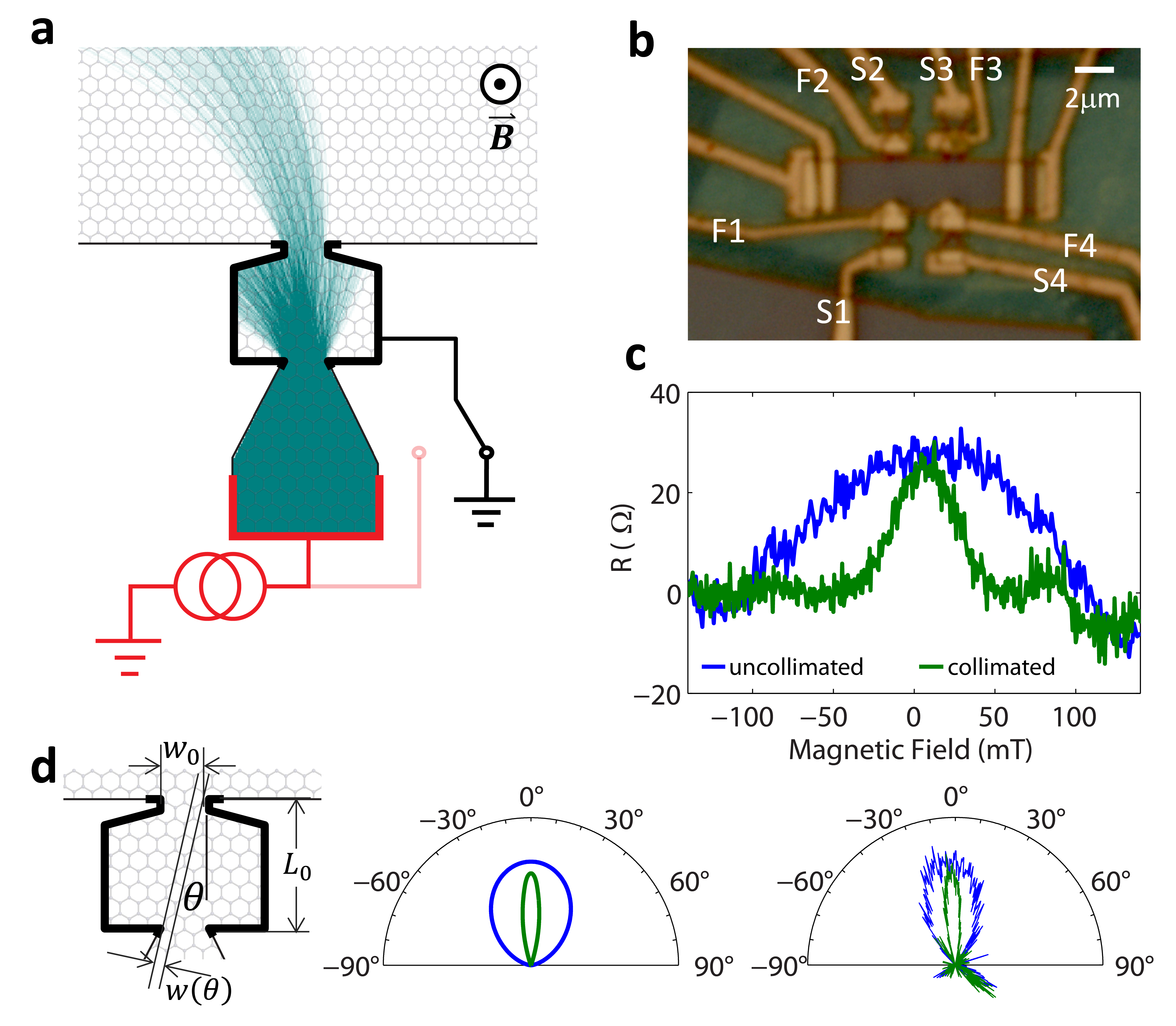
Here, we demonstrate experimentally and validate computationally an electron collimator based on a collinear pair of pinhole slits in hBN-encapsulated graphene. We show that grounded edge contacts[20] – analogous to peripheral surfaces painted black in an optical system – can efficiently remove stray electron trajectories that do not directly traverse the two pinholes, leaving a geometrically defined collimated beams. An absorptive pinhole collimator is constructed from an etched graphene heterostructure with a two-chamber geometry wherein independent electrodes make ohmic contact to each chamber (Fig. 1a). The contact to the bottom chamber (red, Fig. 1a) serves as the source for charge carriers while the contact to the top chamber (black, Fig. 1a) acts as an absorptive filter. To realize a collimating configuration, the filter contact (F) is grounded and the source contact (S) is current-biased; charge carriers are isotropically injected from the source, but only those trajectories that pass through both pinhole apertures reach the graphene bulk. Applying a uniform magnetic field can steer the collimated beam. For an uncollimated configuration, the filter and source contacts are electrically shorted.
Our device consists of hBN-encapsulated graphene etched into a hall-bar-like geometry with the voltage probes replaced by collimating contacts (Fig. 1b). The hBN layers are both thick and the device is assembled on atop a degenerately doped silicon substrate used as a back gate to tune charge carrier density n. To test the collimation behavior of an individual injector in the ballistic regime, we perform a nonlocal magnetotransport measurement, injecting from one collimator and probing trajectories that reach across the width of the device () in the collimated and uncollimated configurations (green, blue respectively, Fig. 1c). We inject from the lower right collimator (labeled S4,F4) throughout this Letter and in this case, measure the voltage of the upper right collimator (labeled S3,F3) relative to a reference (F1). In the presence of a B-field, electron trajectories that pass from the injector to collector flow from the injector at an angle , where is the quasiparticle charge. From this, we find that the angular full width at half maximum (FWHM) is when injecting in the uncollimated configuration and 18⁰ when injecting in the collimated configuration.
For an uncollimated source[3], the angular conductance is expected to go as where is the flux density at the Fermi level, and is the projected width of the contact. The collector has an acceptance angle of , leading to an expected distribution (). The FWHM for our uncollimated data is in reasonable agreement with this expectation given that the reference contact collects more electrons at higher B-fields and thus suppresses the signal at high angles.
In our collimators, the flux density at the Fermi level is identical to that in a single slit, but the projected width is geometrically defined by the pinhole width and pinhole separation . For small angles , the projected width (left, Fig. 1d). At larger angles, no carriers should transmit, yielding:
| (1) |
Convolving over the acceptance angle of the collector (see Supplementary Information for details), we calculate the angular conductance distribution (middle, Fig. 1d) for both the uncollimated case (blue) and the collimated case (green) with and , consistent with the fabricated collimator dimensions. The FWHM of the collimator emission is for theory and for experiment (right, Fig. 1d); showing that our injectors efficiently filter wide-angle trajectories and transmit narrowly collimated beams.
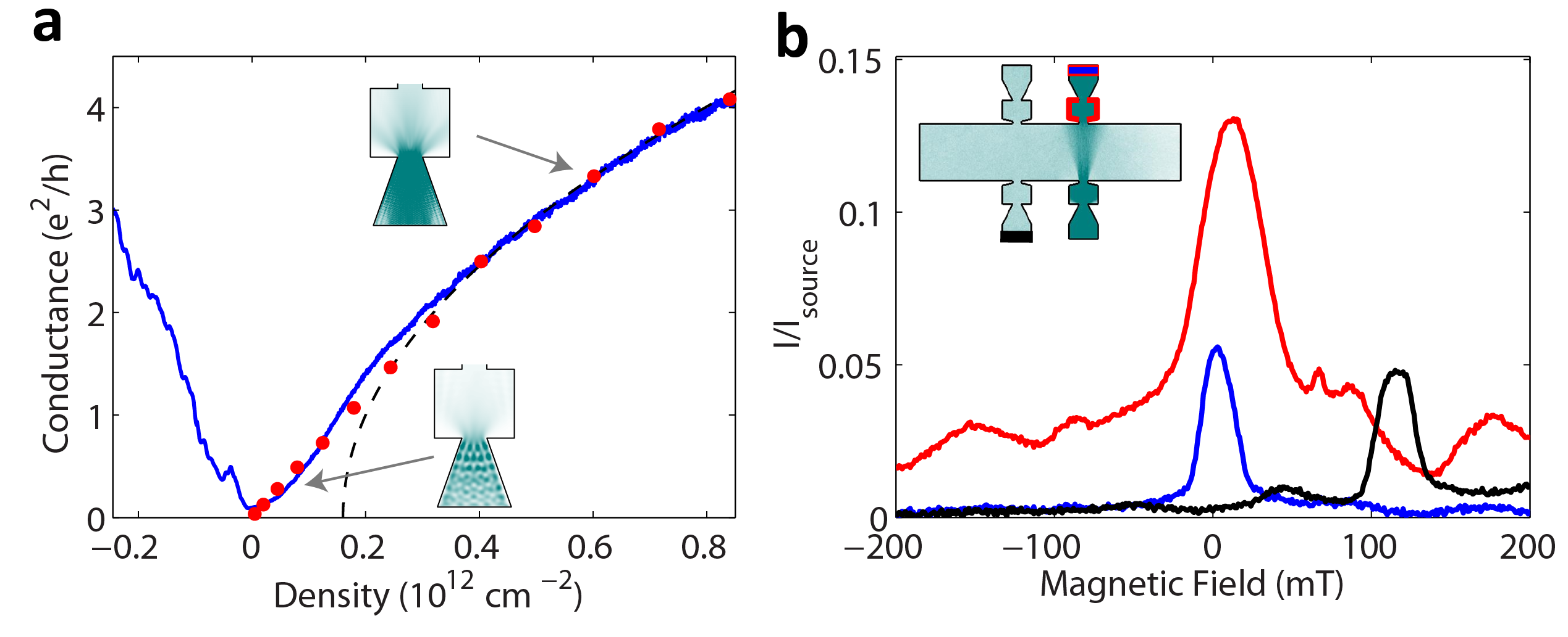
Having established that the angular distribution of injected charge carriers is well-described by semiclassical theory, we now measure our collimators’ conductance to determine how efficiently electrons traverse the pinholes. For this, we bias the injector in the collimating configuration (F4 grounded) and measure the current reaching all remaining electrodes as a function of gate voltage (Fig. 2a). The conductance of the collimator tunes sublinearly with n: (dotted line, Fig 2a). This qualitatively agrees with semiclassical expectations : integrating equation (1) over all angles, we expect
| (2) |
The small offset in our measurement appears to result from diffraction by collimator slits (Fig. 2a, see Supplementary Information for details). Comparing equation (2), with the fit in Fig. 2a (neglecting ), indicates a conductance that is 35% of expectations. This is a lower bound for the transmission probability, because the collimating filter (F4) can reabsorb electrons that have diffusely scattered off of device edges.
To understand the impact of diffuse scattering and better estimate the transmission probability, we measure the current collected at specific detectors as a function of B-field. Having sourced , we collect current in detectors collinear with (red, blue, Fig. 2b) and adjacent to (black, Fig. 2b) the injector. Current collected at the collinear detector with a wide acceptance angle (red) peaks near since the collimated beam travels straight across the device. The apparent background current is 3-5% of . At , ballistic cyclotron orbits instead reach the adjacent detector, leading to a prominent peak in current detected at S1 (black) with F1 grounded. Coincident with this peak, the diffuse background of the collinear detector dips since ballistic trajectories are consumed by the adjacent detector, reducing the number of electrons that eventually find their way into the collinear detector.
In light of the nontrivial diffuse background, we measure current with a narrow acceptance angle at the collector, rejecting most scattered electrons and thus better determining the transmission probability of the collimator. The resulting doubly-collimated beam (blue) has a FWHM of . Together all these collinear apertures act as a single collimator with (the separation between the farthest-apart apertures). All of the injected current passes through the first aperture, so the fractional current collected should be . The maximum of the doubly-collimated peak is 0.056 (Fig. 2b). Subtracting a background of 0.005-0.015 (see Supplementary Information for details), suggests transmission through the full path is times the expected value. The 20% beamwidth-narrowing observed above for a single collimator ( vs expected) may indicate modest focusing, which would be consistent with slightly-enhanced transmission through the double collimator. The excellent quantitative agreement shows that charge carriers transmit nearly perfectly from slit to slit. By demonstrating not only narrow beams but also high transmission probabilities, our measurements show that absorptive pin-hole filtering could produce low-noise, coherent, collimated beams of electrons in 2DESs that cannot be depleted by electrostatic gating.
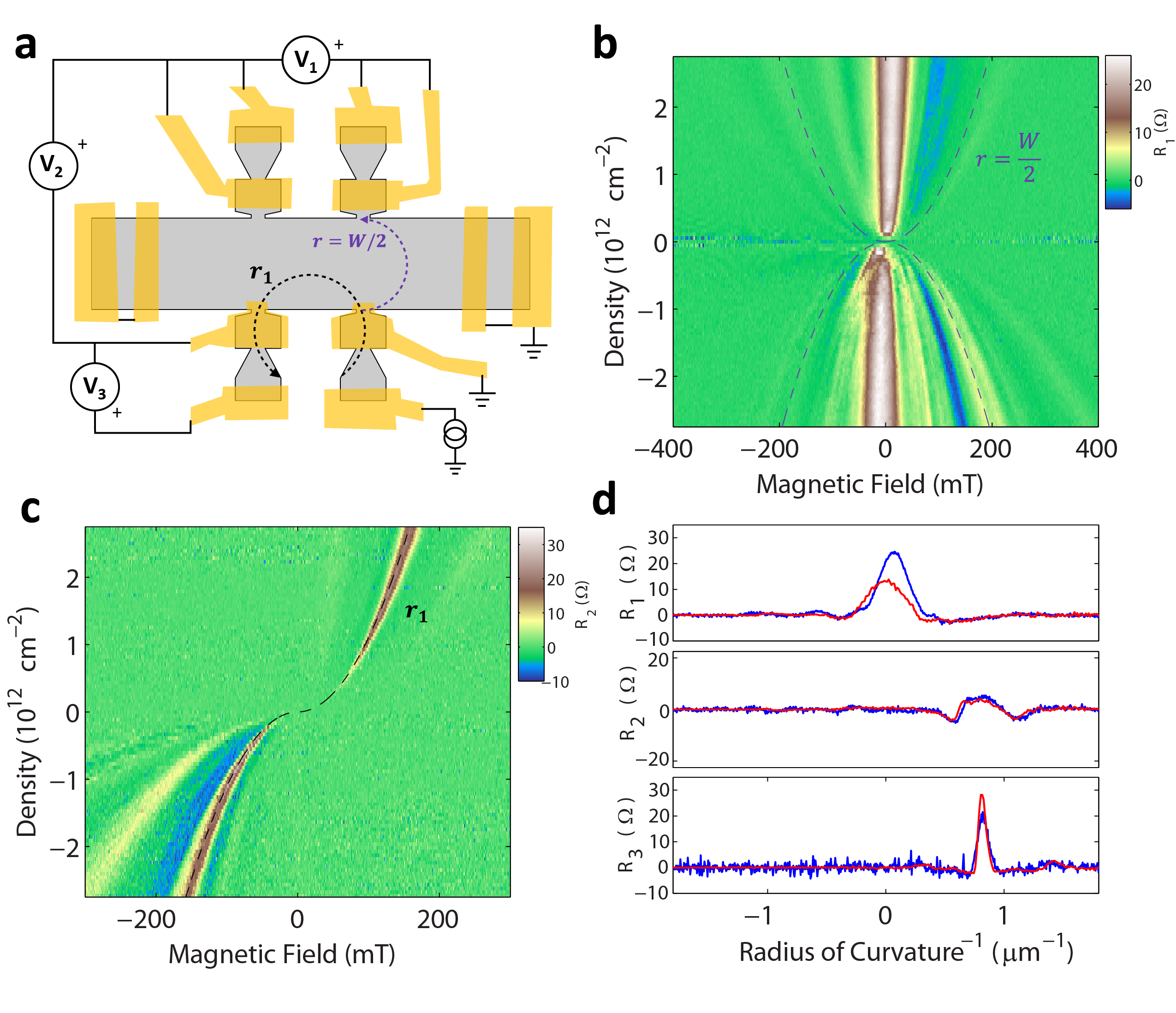
Having experimentally demonstrated that absorptive pinhole collimators can controllably emit electron beams in hBN-encapsulated graphene heterostructures, we illustrate our technology’s utility by aiming a beam at the edges of our graphene device to learn about the low-energy scattering behavior of etched edges in these heterostructures. We perform three simultaneous nonlocal resistance measurements (Fig. 3a) to probe the specularity of reflections off various edges of the device. In Fig. 3b, we map as a function of B-field and electron density. In both the electron-doped and hole-doped regimes, a peak near corresponds to ballistic quasiparticles being collected by the collinear contact in the absence of magnetic deflection. Peaks in also appear at higher fields, primarily in the hole-doped regime (n¡0). For reference, we plot contours corresponding to cyclotron radius . Any features outside the parabolas cannot correspond to direct ballistic quasiparticle transport across the width of the device, and must involve scattering. These data imply that holes undergo multiple reflections at high B-fields, suggesting that the edges may scatter more specularly when hole-doped than when electron-doped.
To directly probe the specularity of reflections in our device, we perform a collimated transverse-electron focusing (TEF) measurement.[4, 29] Probe at the lower left detector is even more sensitive than traditional TEF measurements to scattering that modifies ballistic trajectories, since here the injector and detector have narrow emission and acceptance angles respectively. as a function of electron density and B-field has several distinct features associated with specific cyclotron radii (Fig. 3c), particularly for hole doping. At there is a sharp peak with a FWHM of in both the hole and electron regimes. Though a conventional TEF peak would occur at where is the lateral separation of injector and detector, our measured peak corresponds to slightly greater cyclotron radius. This is expected for our collimator geometry: we illustrate the expected trajectory in Fig. 3a and plot its corresponding contour in Fig. 3c, indicating excellent agreement with our measurement (see also Supplementary Information for calculation). Trajectories at are insensitive to edge scattering, while at smaller r (larger B), additional peaks imply specular reflection. In the electron-doped regime, the presence of a prominent peak at with no appreciable secondary peak suggests completely diffuse scattering, while in the hole-doped regime, the presence of a significant secondary peak suggests appreciable specular reflection.
To validate this understanding and quantitatively determine the degree of specularity, we next carry out semiclassical, device-scale simulations. Modeling the fabricated device geometry including all ohmic contacts, we simulate electron emission from the injector, allowing for reflection off edges, and interaction with floating or grounded ohmics. With two free parameters, transmission of ohmics and probability of diffuse edge scattering , we simulate the measurement configuration shown in Fig. 3a-c (see Supplementary Information for simulation details). The striking similarities between simulation ( and ) and measurement suggest that edge scattering is diffuse in our device in the electron-doped regime (Fig. 3d, see Supplementary Video 1 for visualizing a B-sweep). Similar analysis yields and in the hole-doped regime, quantitatively demonstrating significant electron-hole asymmetry in both ohmic contact properties and specularity of edge scattering in our device
The strong agreement between semiclassical theory and experiment for both individual collimators and our entire collimating device indicates that absorptive collimation in high-mobility graphene devices can be predictably and robustly applied in a variety of geometries, opening the door for scientific and technological use of narrow electron beams in 2DESs. For example, Klein tunneling[7, 8] and Andreev reflections[30] are highly angularly-dependent phenomena whose experimental signatures are obscured in typical transport experiments. In such cases, collimation-based measurements will illuminate the physics by quantitatively testing transmission and reflection at specific angles rather than integrated over a range of angles as in past experiments. In addition, novel technologies such as ballistic magnetometers may be built on the sharp magnetotransport features we achieve. Collimated sources are an important addition to the growing toolbox of electron-optical elements in ballistic graphene devices that enable a new class of transport measurements.
0.1 Sample Fabrication
Flakes of graphene (from highly oriented pyrolytic graphite, Momentive Performance Materials ZYA grade) and of hBN (from single crystals grown by high-pressure synthesis as in Ref. 21) were prepared by exfoliation (3M Scotch 600 Transparent Tape) under ambient conditions (35-60% relative humidity) on n-doped silicon wafers with 90 nm thermal oxide (WRS materials). The heterostructure was assembled by a top-down dry pick-up technique as described in (20). The completed heterostructure was deposited on a chip of n++-doped silicon with 300 nm thermal oxide (WRS materials). Polymer residue from the transfer process was removed by annealing the sample in a tube furnace for 1 h at 500 C under continuous flow of oxygen (50 sccm) and argon (500 sccm). Device patterns were defined by e-beam lithography and reactive ion etching as described in (13). Ohmic contacts were established to the device using electron-beam evaporated Cr/Au electrodes to the exposed graphene edge as described in (20).
0.2 Measurement
All measurements were performed at 1.6K in the vapor space of a He flow cryostat with a superconducting magnet. Lock-ins (Stanford Research Systems SR830) at 17.76 Hz were used in all measurements; voltages were measured with Stanford Research Systems SR 560 voltage preamplifiers and currents were measured with Ithaco 1211 current preamplifiers. The charge density n was calculated from Shubnikov-de-Haas oscillations , in good agreement with the expected geometric capacitance.
References
- [1] Oliver, W. D., Kim, J., Liu, R. C. & Yamamoto, Y. Hanbury Brown and Twiss-Type Experiment with Electrons. Science 284, 299–301 (1999).
- [2] Henny, M. et al. The Fermionic Hanbury Brown and Twiss Experiment. Science 284, 296–298 (1999).
- [3] Molenkamp, L. W. et al. Electron-beam collimation with a quantum point contact. Physical Review B 41, 1274–1277 (1990).
- [4] van Houten, H. et al. Coherent electron focusing with quantum point contacts in a two-dimensional electron gas. Physical Review B 39, 8556–8575 (1989).
- [5] Zhang, Y., Tan, Y.-W., Stormer, H. L. & Kim, P. Experimental observation of the quantum Hall effect and Berry’s phase in graphene. Nature 438, 201–204 (2005).
- [6] Novoselov, K. S. et al. Electric Field Effect in Atomically Thin Carbon Films. Science 306, 666–669 (2004).
- [7] Katsnelson, M. I., Novoselov, K. S. & Geim, A. K. Chiral tunnelling and the Klein paradox in graphene. Nature Physics 2, 620–625 (2006).
- [8] Young, A. F. & Kim, P. Quantum interference and Klein tunnelling in graphene heterojunctions. Nature Physics 5, 222–226 (2009).
- [9] Mayorov, A. S. et al. Micrometer-Scale Ballistic Transport in Encapsulated Graphene at Room Temperature. Nano Letters 11, 2396–2399 (2011).
- [10] Rickhaus, P. et al. Ballistic interferences in suspended graphene. Nature Communications 4, 2342 (2013).
- [11] Shytov, A. V., Rudner, M. S. & Levitov, L. S. Klein Backscattering and Fabry-P\’erot Interference in Graphene Heterojunctions. Physical Review Letters 101, 156804 (2008).
- [12] Lee, G.-H., Park, G.-H. & Lee, H.-J. Observation of negative refraction of Dirac fermions in graphene. Nature Physics 11, 925–929 (2015).
- [13] Lee, M. et al. Ballistic miniband conduction in a graphene superlattice. Science 353, 1526–1529 (2016).
- [14] Chen, S. et al. Electron optics with p-n junctions in ballistic graphene. Science 353, 1522–1525 (2016).
- [15] Nakaharai, S., Williams, J. R. & Marcus, C. M. Gate-Defined Graphene Quantum Point Contact in the Quantum Hall Regime. Physical Review Letters 107, 036602 (2011).
- [16] Sivan, U., Heiblum, M., Umbach, C. P. & Shtrikman, H. Electrostatic electron lens in the ballistic regime. Physical Review B 41, 7937–7940 (1990).
- [17] Hartmann, R. R., Robinson, N. J. & Portnoi, M. E. Smooth electron waveguides in graphene. Physical Review B 81, 245431 (2010).
- [18] Williams, J. R., Low, T., Lundstrom, M. S. & Marcus, C. M. Gate-controlled guiding of electrons in graphene. Nature Nanotechnology 6, 222–225 (2011).
- [19] Stormer, H., Dingle, R., Gossard, A., Wiegmann, W. & Sturge, M. 2-Dimensional Electron-Gas at a Semiconductor-Semiconductor Interface. Solid State Communications 29, 705–709 (1979).
- [20] Wang, L. et al. One-Dimensional Electrical Contact to a Two-Dimensional Material. Science 342, 614–617 (2013).
- [21] Dean, C. R. et al. Boron nitride substrates for high-quality graphene electronics. Nature Nanotechnology 5, 722–726 (2010).
- [22] Taychatanapat, T. et al. Conductance oscillations induced by ballistic snake states in a graphene heterojunction. Nature Communications 6, 6093 (2015).
- [23] Rickhaus, P., Makk, P., Liu, M.-H., Richter, K. & Schönenberger, C. Gate tuneable beamsplitter in ballistic graphene. Applied Physics Letters 107, 251901 (2015).
- [24] Wilmart, Q. et al. A Klein-tunneling transistor with ballistic graphene. 2D Materials 1, 011006 (2014).
- [25] Yamamoto, M. et al. Electrical control of a solid-state flying qubit. Nature Nanotechnology 7, 247–251 (2012).
- [26] Bautze, T. et al. Theoretical, numerical, and experimental study of a flying qubit electronic interferometer. Physical Review B 89, 125432 (2014).
- [27] Park, C.-H., Son, Y.-W., Yang, L., Cohen, M. L. & Louie, S. G. Electron Beam Supercollimation in Graphene Superlattices. Nano Letters 8, 2920–2924 (2008).
- [28] Cheianov, V. V., Fal’ko, V. & Altshuler, B. L. The Focusing of Electron Flow and a Veselago Lens in Graphene p-n Junctions. Science 315, 1252–1255 (2007).
- [29] Taychatanapat, T., Watanabe, K., Taniguchi, T. & Jarillo-Herrero, P. Electrically tunable transverse magnetic focusing in graphene. Nature Physics 9, 225–229 (2013).
- [30] Efetov, D. K. et al. Specular interband Andreev reflections at van der Waals interfaces between graphene and NbSe2. Nature Physics 12, 328–332 (2016).
We thank M. Lee and T. Petach for fruitful discussions. This work was financially supported by the Gordon and Betty Moore Foundation through Grant GBMF3429, by a Nano- and Quantum Science and Engineering Postdoctoral Fellowship (A.B.), by a Ford Foundation Predoctoral Fellowship (A.S.) and a National Science Foundation Graduate Research Fellowship (A.S.). K.W. and T.T. acknowledge support from the Elemental Strategy Initiative conducted by the MEXT (Japan). T.T. acknowledges support from JSPS Grant-in-Aid for Scientific Research under grants 262480621 and 25106006. Part of this work was performed at the Stanford Nano Shared Facilities (SNSF).
A.B., D.G.-G., A.H., and A.S. conceived of the measurements. A.S. fabricated the device. A.B., A.H., and A.S. performed transport measurements. A.B. and A.H. performed numerical simulations. A.B. wrote the manuscript with input from all other authors. K.W. and T.T. grew the bulk hBN crystals.
The authors declare that they have no competing financial interests.
Correspondence and requests for materials
should be addressed to
A.B. (email: barnarda@stanford.edu) or D.G.-G. (email: goldhaber-gordon@stanford.edu).
 \spacing
1
 \spacing
1
 \spacing
1
See pages - of SI_Collimator_NNano.pdf