Limitations of the intrinsic cut-off frequency to correctly quantify the speed of nanoscale transistors
Abstract
The definition of the intrinsic cut-off frequency () based on the current gain equals to one (0 dB) is critically analyzed. A condition for the validity of the quasi-static estimation of is established in terms of the temporal variations of the electric charge and electric flux on the drain, source and gate terminals. Due to the displacement current, an electron traversing the channel length generates a current pulse of finite temporal width. For electron devices where the intrinsic delay time of the current after a transient perturbation is comparable to such width, the displacement currents cannot be neglected and the quasi-static approximation becomes inaccurate. We provide numerical results for some ballistic transistors where the estimation of under the quasi-static approximation can be one order of magnitude larger than predictions obtained from a time-dependent numerical simulations of the intrinsic delay time (including particle and displacement currents). In other ballistic transistors, we show that the gate current phasor can be smaller than the drain one at all frequencies, giving no finite value for .
Index Terms:
Cut-off frequency, THz, displacement current, nano transistor, time-dependent simulation.I Introduction
The development of faster electron devices for digital and analog applications is a constant demand in the electronics industry [1, 2].The scientific community tries to quantify how fast the field effect transistors (FETs) work through some figures of merit (FoMs). Unfortunately, there is no such a unique FoM that unequivocally quantifies the speed. Some definitions are linked to a particular circuit or application, others to the intrinsic device itself. Some FoMs are redefined to make them more easily accessible from simulations, or from measurements. Usually, the FoM in digital FET applications are related with times, while in analog ones are commonly described with frequencies.
In digital FET applications, for example, an important FoM is the intrinsic delay time . The idea of this FoM is to quantify the time needed for an output signal to respond to an input signal[3]. Many times, a simpler quasi-static definition of the intrinsic delay time, , is preferred because it is easily accessible from DC (time-independent) simulations [1]. Such expression can be interpreted as the time needed to charge the next gate capacitor until the gate voltage associated to the ON state, with a constant drain-source current . From an experimental point of view, however, a new definition of the intrinsic delay time from a ring oscillator of (odd) CMOS inverters is used. By taking the inverse of the frequency at which the ring oscillator runs and dividing it by , such intrinsic delay time can be easily obtained [4].
In analog applications, the cut-off frequency and the maximum oscillation frequency are the main FoMs. The is defined as the frequency at which the drain and gate currents become equal (that is a current gain of 0 dB) [5, 6]. Equivalently, the is the frequency at which the power gain is 0 dB [1]. Both frequencies are easily accessible from the measurement of -parameters and even their intrinsic values (when all parasitic elements of the circuit are eliminated using de-embedding techniques) are measurable. Needless to say, , based on Mason’s identities [7], becomes a more relevant FoM in high-frequency analog applications [2].
It is accepted that, although the intrinsic is not the relevant FoM in high frequency analog applications, it is a meritorious FoM providing useful information on the speed of FETs. In order to provide an expression of the cut-off frequency accessible from DC (time-independent) simulations, the so-called quasi-static approximation is presented in the literature [9, 10, 8, 11, 12]. It is based on assuming that the drain current is only the DC component related to the (linear) transconductance , while the gate current is the displacement component proportional to the capacitor and frequency. From the previous quasi-static definition of the intrinsic delay time in digital applications, we easily arrive to the approximation [13, 14]. This last expression supposedly justifies why the cut-off frequency is a good FoM to quantify the intrinsic switching speed in digital applications. Alternatively, several non-quasi-static approximations are also proposed for more accurate predictions of [6, 8, 15, 16].
In this paper, we discuss if can be an appropriate FoM to quantify the intrinsic speed of these nanoscale FETs with dimensions of few nanometers for digital or analog TeraHertz (THz) applications. In such FETs, the electric field generated by an electron crossing the channel is not properly screened and it induces displacement current on the terminals. We will construct a condition for the validity of the quasi-static estimation of and prove that can be a quite misleading estimator (with or without approximations) for the speed of ballistic FETs.
We summarize here four relevant time intervals that will be used along the paper. The intrinsic delay time quantifies the temporal difference between the time when a gate voltage perturbation starts and the time when the gate, drain and source currents reach steady-state values. The and are the intrinsic delay time mentioned above under the quasi-static approximation and under the zero-order non-quasi-static approximation, respectively. Due to the displacement current, one electron traversing the channel length generates a current pulse 111In the case of an electron with charge and velocity moving between two infinite parallel metals separated with a distance , it is well known from the Ramo-Shockley-Pellegrini theorem [17] that the square pulse current has a temporal width of and a height equals to . The total charge of the current pulse is .. The temporal width of such pulse is defined as . The value of is influenced by the device geometry and the dielectric relaxation time needed for the background charge to neutralize (screen) the electric field generated by the single electron. In the text, we also define , and as the cut-off frequencies associated to , and , respectively. Finally, is the exact definition of the cut-off frequency from the current gain equals to one. We will see in this paper that can differ from .
II Fourier Analysis of
In this Section, a Fourier analysis of the definition of from the current gain equals to one will be discussed, with special attention to the role played by the particle and displacement currents on it. This complete discussion is valid for any type of (ballistic or non-ballistic) FETs. We will also present the conditions of validity of the quasi-static approximation in terms of the temporal variations of the electric charge plus the electric flux on the drain, source and gate terminals.
II-A Preliminary Discussion
We consider a dual-gate FET depicted in Fig. 1(a) with three terminals. The three relevant total (displacement plus particle) currents, named , and are associated to the gate, drain and source terminals, respectively, as
| (1) |
being the electric permittivity, the electric field and the particle current density. We consider outwards. The three surfaces in equation (1) construct a surface that totally enclose an arbitrary volume . Then, by construction, at any time , the three currents satisfy
| (2) |
which is just the conservation of the total current in the active region due to the application of Gauss’s law in .
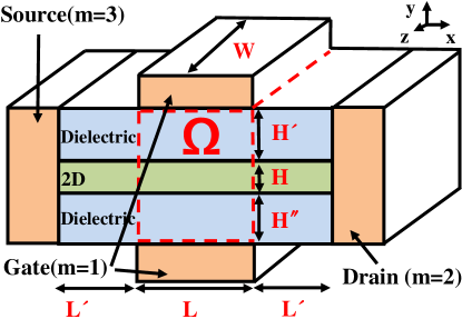
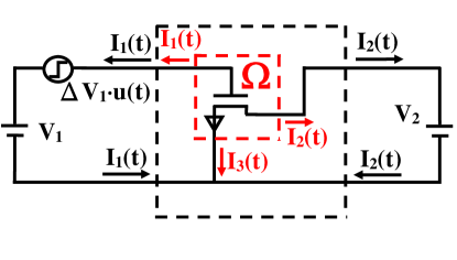
In the evaluation of , we are interested in a transient simulation. Initially, the three currents have steady-state values . At , a (small-signal) voltage perturbation is applied on one of the three FET terminals. Then, during a time interval (we will see later that this time is indeed the intrinsic delay time), the three output currents oscillate. Finally, new steady-state values for the three currents are achieved with for . For each contact , we define the incremental charge during as
| (3) |
Using (2) that ensures at any time, we easily get
| (4) |
This equation just states that the variation of electron charge from till in the volume is compensated by the variations of the electric flux during this time interval on the surface .
II-B The All-order Definition of
The usual definition of comes from a FET in common source configuration as plotted in Fig. 1(b). Following the signs of the currents assigned to the FET of Fig. 1(a), the currents on the gate and drain terminals of the two-port network are positive when leaving the network. In the two-port network model of Fig. 1(b), the relationship between the phasor voltages , the phasor currents and the -parameter matrix is
| (5) |
where is the angular frequency and is the Fourier transform. The frequency-dependent component of the admittance matrix, due to a small signal current collected on contact when a step perturbation (with the Heaviside step function) is applied on contact and zero volts in the rest of terminals, is given by [5, 18]
| (6) |
where . In expression (6), we have considered for .
II-C The Quasi-static Definition of
The expression of within the quasi-static approximation is obtained by computing the term from (6) without any frequency dependence, , as
| (8) |
The term is computed with a zero-order approximation, , from (6) as
| (9) |
where is defined in (3). The approximation in (8) is based on the assumption that the current pulse is short enough to neglect any displacement component of the drain current. Expression (9) assumes that the gate current is the displacement component. As indicated in the Introduction, from (7), using (8) and (9) , we get
| (10) |
where the term is usually associated to the gate capacitor [19]. If we assume that , during the transient evolution
| (11) |
we get the condition where is the typical quasi-static definition of the intrinsic delay time mentioned in the Introduction when giving . Then, the definition of the (small-signal) transconductance in equation (8), with expression (11), can be redefined as [13]
| (12) |
Putting (12) into (10), one arrives to the final result
| (13) |
which is one of the main reasons why is interpreted as a relevant FoM on how fast a digital FET works. In summary, the quasi-static approximation is valid whenever the condition is satisfied. From (4), such condition can be equivalently written as . From (3), the previous conditions in a transient evolution means that the source current rapidly becomes equivalent to its high value while the drain current remains low during the intrinsic delay time interval . These conditions are typical in many FETs with a large channel length where the intrinsic delay time is much larger than the temporal width of the current pulse generated by one electron , i.e. . Then, the total (particle and displacement) current in the drain and source contacts are detected only when electrons cross the surfaces and , respectively. However, in FET devices with a short channel length , one can easily get scenarios with where an electron moving along the channel generates a time-dependent electric field that is detected as displacement current on the source and drain contacts without even crossing the surfaces (drain contact) and (source contact).
II-D The Zero-order Non-quasi-static Definition of
In order to better include the drain displacement current, it seems more appropriate to use the same zero-order approximation of the exponential term, , that we have used for in (9), in the computation of from (6)
| (14) |
where is also defined in (3). Consequently, from (7), a non-quasi-static estimation () of gives [20]
| (15) |
This is a first step (zero-order Taylor approximation) in the evaluation of beyond the quasi-static approximation. In a typical n-type FET, when is positive, we can expect a positive transient current satisfying , while the current on the source is negative and decreases because of the signs selected in Fig 1(b). Since we deal with an increment of electrons (negative charge) in the channel, we expect in the metal. From (3) we get positive and , while negative . Therefore, the expression is achieved, which means . This condition will be numerically tested later. Therefore, the definition of in (15) can be ill-defined because it deals with a square root of a negative number, that is, the condition cannot be reached with this zero-order non-quasi-static approximation.
We arrive now to a relevant question about the adequacy of as a proper FoM for testing FET speed. Is it possible to find FETs where the gate phasor current is always smaller than the drain one, even with the exact definition of the parameters in (7)? This would imply that, contrarily to what is assumed in the own definition of , the current gain never drops to 0 dB at any frequency.
III Numerical simulation
The conditions of validity of were discussed in Section II-C. In Section II-D we pointed out the possibility that the own definition of is ill-defined because there is no guarantee that the gate phasor current becomes higher than the drain phasor current as frequency grows. Next, we provide numerical confirmation of these drawbacks for ballistic nanoscale FETs.
III-A Device Structure and Time-dependent Simulations
We will consider dual-gate FETs schematically drawn in Fig. 1(a) with a 2D channel material. These 2D materials are expected to improve electron mobility and to suppress the short channel effect for ultra-scaled devices. In order to simplify the numerical simulations (avoiding extra complications, like Klein tunneling or hole transport, that will obscure the interpretations of our numerical results), we will consider only electron transport in the conduction band of a n-type graphene-like material with a linear energy band being m/s the Fermi velocity and the wave vector which contains the two degrees of freedom . The permittivity is in the 2D material and in dielectrics with is the vacuum permittivity. Electron transport will be assumed ballistic (without phonon or impurity scattering) and only the electron-electron interaction through the Poisson equation will be considered. The simulation box will not include the 3D-2D contact resistances and other parasitic elements (which are the well-known frequency bottleneck [1]). Thus, we only simulate the intrinsic performance of FETs.
We will consider FET devices with a width of the current pulse associated to one electron comparable to the intrinsic delay time along the channel, i.e. . These conditions just mean that the channel is short enough and the dielectric relaxation time large enough so that the displacement current of an electron crossing the channel has to be considered in each terminal even when the electron is in the middle of the channel. The extension depicted in Fig. 1(a) is present to ensure the proper computation of such displacement current, even when the electrons are outside of the volume . The time-dependent total currents in equation (1) are computed with the BITLLES simulator [21] from self-consistent Monte Carlo solutions of the Boltzmann and Poisson equations. The temporal step of the simulations is s. Finally, we notice that all the transient simulations have been repeated many times and the results properly averaged in order to minimize the presence of physical noise [22] (random fluctuations) in the current values. The reasons are to avoid extra non-pertinent complexities in the discussions of the results and to approach experimental -parameters setups which provide measurements through several periods of the oscillating signals.
III-B Example 1: Device A
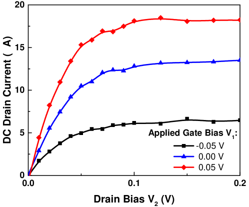
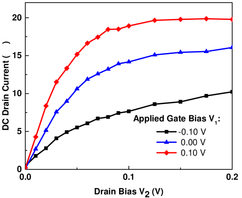
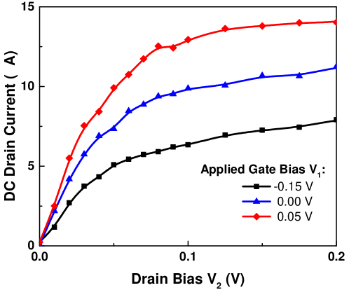
We consider device A with a volume in Fig. 1(a) with the 2D material thickness nm and the gate length nm. In the simulation box, we set spatial steps nm, nm and nm resulting cells. The DC characteristic plotted in Fig. 2 is computed by time-averaging the total drain current in (1) and by summing the net number of electrons transmitted through the drain surface. Both DC values coincide because the time-averaged displacement current is zero. Such double computation of the drain DC value certifies the correct simulation of the displacement current.
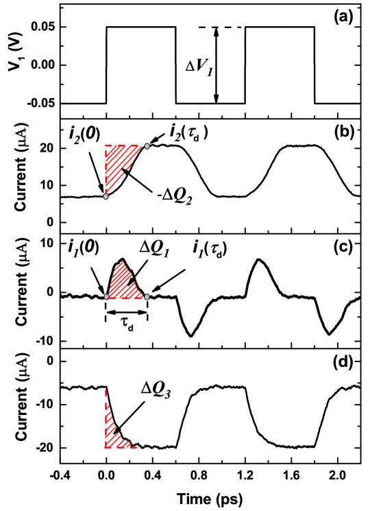
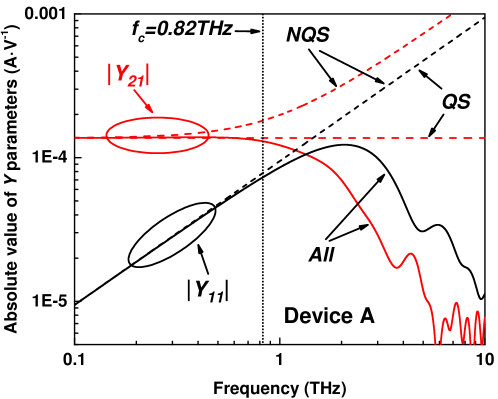
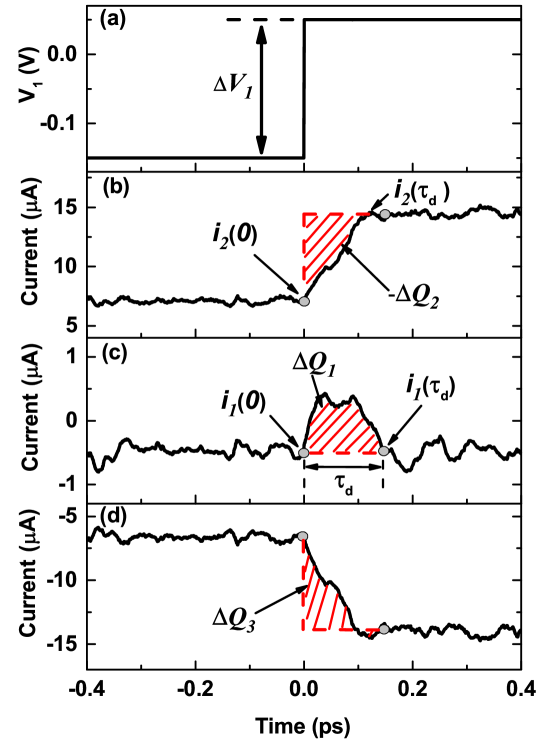
The transient currents in response to two square voltage pulses on the gate contact are indicated in Fig. 3. As illustrated in Fig. 1(b), since we deal with a small-signal formalism, the evaluation of and is done with a DC bias, V, applied between drain and source contacts, and a DC voltage V plus the transient perturbation V on the gate. In Fig. 4, the solid lines are and computed exactly from (6) as a function of frequency. For frequencies higher enough, the absolute value of shows strong frequency dependency and the is no longer linearly increasing with the frequency, which is qualitatively identical to the experimental observations [19]. The values of and become equal at THz.
Using the quasi-static approximation in expression (10), we get THz, which is similar to the previous value THz. In the non-quasi-static approximation, the formula (15) requires the restriction . As illustrated in Fig. 3 (red dashed area), C, C and C. The result is coincident with what we anticipated in Section II-D. Since , there is no solution to the in non-quasi-static case. This result can also be understood from (14) indicating that controls the frequency slope of at high enough frequencies. Similarly, from (9), the slope of is controlled by the . Since , the terms and never cross as can be seen in Fig. 4. Surprisingly, the (zero-order) non-quasi-static model is even worse than the simpler quasi-static one.
The errors when neglecting the displacement current in the computation of can be quantified from expression (14). The elimination of the drain displacement current can be justified for those frequencies satisfying that is larger or equal than the . By imposing the previous condition, , we get a definition of the maximum frequency where the drain displacement current can be reasonably neglected
| (16) |
However, since we have demonstrated in equation (4) that , we always get which can be seen in Fig. 4 where solid lines (All) start to deviate from dashed lines (QS) at THz THz. Notice that the condition in (16) implies that justifying the arguments on the range of validity of mentioned in Section II-C.
III-C Example 2: Device B
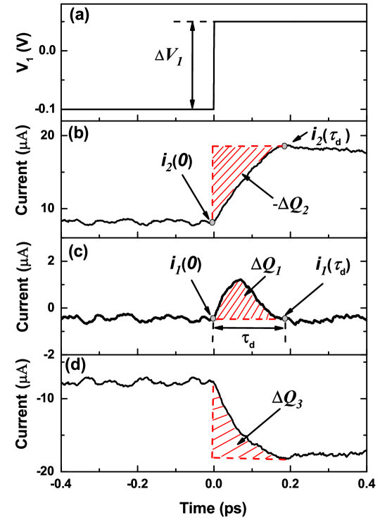
The quasi-static approximation seems to imply that a desired condition for a fast FET is () if short channel effects are still under control. Such condition would imply that in equation (10) and . We consider a new design (device B) with the goal of getting . In particular we consider the same FET of Fig. 1(a) with the geometry (gate length nm) under the same type of simulation as in device A. In the simulation box, we set spatial steps nm, nm and nm resulting cells. We plot the DC current-voltage characteristic of device B in Fig 5. In spite of the small capacitance, the short channel effects are reasonably under control. We use V, applied between drain and source contacts, and V plus the transient perturbation V on the gate. The total transient currents on the drain, gate and source contacts of device B due to a step voltage perturbation in the gate are plotted in Fig. 6, where the sum of the total currents also maintains consistency with the continuity equation (2). Moreover, the incremental charge C, C and C.
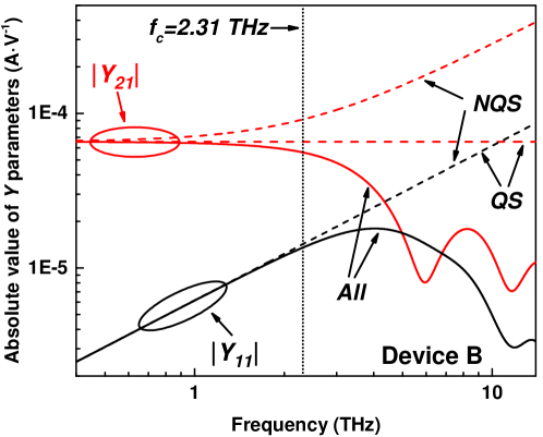
The parameters changing with frequency in all orders (solid lines), NQS and QS models (dashed lines) for device B are plotted in Fig. 7. In the quasi-static estimation, because the in device B becomes smaller than that of device A, the is shifted towards the horizontal axis, therefore, the quasi-static value of the cut-off frequency increases giving THz. The behaviors of NQS for device B and device A are similar. In the all orders model, the condition is satisfied at THz. The oscillations of and at higher frequencies are the Fourier transform of time-dependent variations of the total currents in Fig. 6, which can be associated to plasmonic oscillations with shorter periods than the value of plotted there. So the exact value of the is randomly influenced by such oscillations. We have assumed an ideal metallic contact (dielectric relaxation time equals to zero) in all simulations. One can expect significantly different randomness in the oscillations of the parameters at high frequency for heavily doped contacts [23]. The problem present in device B is that the real frequency where the device stops working properly is much lower than THz and THz.
III-D Example 3: Device C
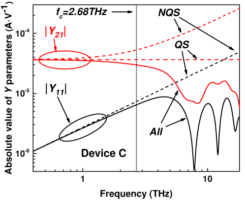
To go a step further, we design a device C which has volume (gate length nm). The DC current is plotted in Fig. 8, which indicates the ability of the gate to control the channel. In the transient current plotted in Fig. 9 in response to a step voltage perturbation, we get the incremental charge C, C and C. The approaches to 0. The parameters are plotted in Fig. 10. The QS result THz is quite far from the maximum frequency THz. It is relevant to emphasize that the condition is never satisfied in the whole THz window for the all orders model, i.e. the and never cross, showing a misleading result . Certainly, the real nano FET stops working properly at some frequency.
To understand the real speed limitation of devices B and C, let us notice that the simulations in Figs. 3, 6 and 9 can be interpreted in two different ways. First, as we have done up to here, the currents are the FET response to a step voltage perturbation needed for computing the small-signal -parameter in a linear system. Second, they can be identically interpreted as the current response when the gate change from the digital voltage ‘0’ to ‘1’. Then, the time defined in expression (3) is directly related to the intrinsic delay time discussed in the Introduction as a FoM for digital electronics. In other words, the two pulses in Figs. 3(a) can be understood as the input digital signal and the drain currents as the output digital signals. Certainly, the FETs are not properly switched-off in our small-signal simulations, and a large-signal simulation will be needed, in principle. However, the present simulations are enough to compare the different FET speed estimators. The relation between the input and output signals in Figs. 3, 6 and 9 can be modeled from linear system theory. It is clear that the relevant frequencies are inversely proportional to the time interval . A reasonable expression could be [24] [25].
In device A, from Fig. 3, we get a value of the intrinsic delay time ps, resulting THz, which is similar to the quasi-static cut-off frequencies THz. However, in device B, from Fig. 6, we get a simulated ps giving THz, which is much smaller that the value THz. In device C, the result is even worse where the intrinsic delay time is ps providing THz. The reason why the quasi-static expression (10) does not capture the real intrinsic delay time in devices B and C is because the approximation is no longer true. In fact, since we looked for , the result gives in (10) much larger than in (16). Let us notice that the quasi-static estimation of the intrinsic delay time is again clearly misleading. In device B, we get ps, which is more than one order of magnitude smaller than our simulated value ps (the ratio is different from because of the factor in (13)). In device C, the ps is also more than one order of magnitude shorter than the simulated value ps. The reason of this discrepancy is also the condition , which invalidates the quasi-static estimation discussed in Section II-C
IV Final discussion and conclusions
In conclusion, we have established the condition for the validity of the quasi-static approximation of in terms of the electrical current and electrical flux on the gate, drain and source FET terminals defined in expressions (1) and (3). Such approximation is applicable when which means that we are dealing with FETs where the intrinsic delay time is much larger than the temporal width of the current pulse generated by one electron, i.e. (with large channel length as in device A). On the contrary, in devices where (i.e. as in devices B and C with short channel length ), the quasi-static approximation is not applicable because the electric field generated by electrons are not screened inside the device active region, and its associated displacement current becomes relevant during all the time while the electron is traversing the channel. We have shown through analytical arguments supported by numerical simulations that the estimations of the intrinsic cut-off frequency based on (with the quasi-static , zero-order non-quasi-static or without approximations ) can provide misleading results for the speed of FETs. This problem is specially severe for nanoscale FETs which are routinely modeled from quantum transport simulators. The explicit quantum simulation of the time-dependent displacement current and demand such huge amount of computational resources [26, 17, 23] that the intrinsic FoM of the speed of such ballistic FET are routinely taken from quasi-static estimations. As shown in some examples in this work, such type of quasi-static estimations can erroneously predict the FET speed by one order of magnitude. Other examples show no finite value of underlying an important limitation of the traditional definition of to properly quantify the speed of FETs. However, when parasitic elements are included in the simulation, one can expect a tendency to recover the validity of the quasi-static approximation ( grows and remains the same) at the price of getting lower FET speed than its intrinsic value.
References
- [1] F. Schwierz, “Graphene transistors,” Nat. Nanotechnol., vol. 5, pp. 487-496, Jul. 2010. DOI: 10.1038/nnano.2010.89
- [2] G. Fiori, F. Bonaccorso, G. Iannaccone, T. Palacios, D. Neumaier, A. Seabaugh, S. K. Banerjee and L. Colombo, “Electronics based on two-dimensional materials,” Nat. Nanotechnol., vol. 9, pp. 768-779, Oct. 2014. DOI: 10.1038/nnano.2014.207
- [3] Y. Taur and T. H. Ning, Fundamentals of Modern VLSI Devices, 2nd ed., pp. 290, New York: Cambridge University Press, 2009
- [4] K. Shohno, K. J. Callanan and M. Hirayama, “47-Stage P-MOS Ring Oscillator Circuit Using the Two-Photomask Fabrication Process,” Jpn. J. Appl. Phys., vol. 17, no. 6, pp. 1133, 1978. DOI: http://dx.doi.org/10.1143/JJAP.17.1133
- [5] S. E. Laux, “Techniques for Small-Signal Analysis of Semiconductor Devices,” IEEE Trans. Electron Devices, vol. 32, no. 10, pp. 2028-2037, Oct. 1985. DOI: 10.1109/T-ED.1985.22235
- [6] L.-F. Wang, L. Li, N.-D. Lu, Z.-Y. Ji, W.Wang, Z.-W. Zong, G.-W. Xu and M. Liu, “An Improved Cut-Off Frequency Model With a Modified Small-Signal Equivalent Circuit in Graphene Field-Effect Transistors,” IEEE Electron Device Lett., vol. 36, no. 12, pp. 1351-1354, Dec. 2015. DOI: 10.1109/LED.2015.2489205
- [7] S. Mason, “Power Gain in Feedback Amplifier,” Trans. IRE Prof. Group Circuit Theory, vol 1, no 2, pp. 20-25, Jun. 1954. DOI: 10.1109/TCT.1954.1083579
- [8] S. Cho, K. R. Kim, B.-G. Park and I. M. Kang, “RF Performance and Small-Signal Parameter Extraction of Junctionless Silicon Nanowire MOSFETs,” IEEE Trans. Electron Devices, vol 58, no 5, pp. 1388-1396, May 2011. DOI: 10.1109/TED.2011.2109724
- [9] S. Venica, F. Driussi, P. Palestri, D. Esseni, S. Vaziri and L. Selmi, “Simulation of DC and RF Performance of the Graphene Base Transistor,” IEEE Trans. Electron Devices, vol. 61, no. 7, pp. 2570-2576, Jun. 2014. DOI: 10.1109/TED.2014.2325613
- [10] D. Logoteta, G. Fiori and G. Iannaccone,“Graphene-based lateral heterostructure transistors exhibit better intrinsic performance than graphene-based vertical transistors as post-CMOS devices,” Sci. Rep., vol. 4, pp. 6607, Oct. 2014. DOI: 10.1038/srep06607
- [11] X. Zheng, M. Guidry, H. Li, E. Ahmadi, K. Hestroffer, B. Romanczyk, S. Wienecke, S. Keller and U. K. Mishra, “N-Polar GaN MIS-HEMTs on Sapphire With High Combination of Power Gain Cutoff Frequency and Three-Terminal Breakdown Voltage,” IEEE Electron Device Lett., vol. 37, no. 1, pp. 77-80, Jan. 2016. DOI: 10.1109/LED.2015.2502253
- [12] Z. Dong and J. Guo, “Assessment of 2-D Transition Metal Dichalcogenide FETs at Sub-5-nm Gate Length Scale,” IEEE Trans. Electron Devices, vol. 64, no. 2, pp. 622-628, Feb. 2017. DOI: 10.1109/TED.2016.2644719
- [13] J. Singh, Semiconductor Devices: Basic Principles, 1st ed., New York: John Wiley & Sons, Inc., 2001
- [14] C. Rutherglen, D. Jain and P. Burke, “Nanotube electronics for radiofrequency applications,” Nat. Nanotechnol., vol. 4, pp. 811-819, Nov. 2009. DOI: 10.1038/nnano.2009.355
- [15] V. Teppati, S. Tirelli, R. Lovblom, R. Flückiger, M. Alexandrova and C. R. Bolognesi, “Accuracy of Microwave Transistor and Extractions,” IEEE Trans. Electron Devices, vol. 61, no. 4, pp. 984-990, Apr. 2014. DOI: 10.1109/TED.2014.2306573
- [16] H. Cuchillo-Sánchez, F. Zárate-Rincón and R. Torres-Torres, “Alternative Determination of the Intrinsic Cut-Off Frequency Applied to a Degraded MOSFET,” IEEE Microw. Wirel. Compon. Lett., vol. 26, no. 9, pp. 693-695, Sept. 2016. DOI: 10.1109/LMWC.2016.2597209
- [17] A. Benali, F. L. Traversa, G. Albareda, M. Aghoutane and X. Oriols, “Improving the intrinsic cut-off frequency of gate-all-around quantum-wire transistors without channel length scaling,” Appl. Phys. Lett., vol 102, no 17, pp. 173506, May 2013. DOI: org/10.1063/1.4803164
- [18] R. W. Hockney and J. W. Eastwood, Computer simulation using particles, CRC Press, 1988
- [19] Y.-H. Cheng and M. Matloubian, “Frequency-dependent resistive and capacitive components in RF MOSFETs,” IEEE Electron Device Lett., vol. 22, no. 7, pp. 333-335, Jul. 2001. DOI: 10.1109/55.930682
- [20] H. M. J. Boots, G. Doornbos and A. Heringa, “Scaling of characteristic frequencies in RF CMOS,” IEEE Trans. Electron Devices, vol. 51, no. 12, pp. 2102-2108, Dec. 2004. DOI: 10.1109/TED.2004.838449
- [21] http://europe.uab.es/bitlles
- [22] Z. Zhan, E. Colomés, A. Benali, D. Marian and X. Oriols, “Time-dependent simulation of particle and displacement currents in THz graphene transistors,” J. Stat. Mech. Theor. Exp., vol 2016, pp. 054019, May 2016. DOI: 10.1088/1742-5468/2016/05/054019
- [23] D. Marian, N. Zanghì and X. Oriols, “Weak Values from Displacement Currents in Multiterminal Electron Devices,” Phys. Rev. Lett. vol. 116, pp. 110404, Mar. 2016. DOI: doi.org/10.1103/PhysRevLett.116.110404
- [24] A. B. Carlson and P. B. Crilly, Communication Systems, 5th ed., pp. 137, New York: McGraw-Hill, 2010
- [25] Y. Tsividis and C. McAndrew, The MOS Transistor, 3rd ed. pp. 367, New York: Oxford University Press, 2012.
- [26] X. Oriols, “Quantum-Trajectory Approach to Time-Dependent Transport in Mesoscopic Systems with Electron-Electron Interactions,” Phys. Rev. Lett., vol 98, pp. 066803, Feb. 2007. DOI: doi.org/10.1103/PhysRevLett.98.066803