The MuPix Telescope: A Thin, high Rate Tracking Telescope
Abstract
The MuPix Telescope is a particle tracking telescope, optimized for
tracking low momentum particles and high rates.
It is based on the novel High-Voltage Monolithic Active Pixel Sensors (HV-MAPS), designed for the Mu3e tracking detector.
The telescope represents a first application of the HV-MAPS technology and
also serves as test bed of the Mu3e readout chain. The telescope consists of up
to eight layers of the newest prototypes, the MuPix7 sensors, which send
data self-triggered via fast serial links to FPGAs, where the data is time-ordered and
sent to the PC. A particle hit rate of per layer could be processed.
Online tracking is performed with a subset of the incoming data.
The general concept of the telescope, chip architecture, readout concept and online reconstruction are described.
The performance of the sensor and of the telescope during test beam measurements are presented.
1 Introduction
The Mu3e Experiment [1] will search for the lepton flavour violating decay of a positive muon into two positrons and one electron with a target sensitivity of 1 in 1016 decays.
A high rate beam of 109 muons/s will be stopped on a passive target. The momentum of the decay particles as well as the vertex will be measured with a thin four layer pixelated detector.
The high rate of low momentum particles (p < 53 MeV/c) requires a new detector
technology: High-Voltage Monolithic Active Pixel Sensors (HV-MAPS), combing the advantages of thin MAPS with the fast charge collection of classical hybrid pixel sensors are chosen for Mu3e.
To integrate the HV-MAPS into a multilayer tracking device, test the
Mu3e readout architecture and for test beam
characterization of the MuPix sensor prototypes, a tracking telescope has been
build which is discussed in the following.
2 Telescope Concept
General Concept
The MuPix telescope [2] consists of up to eight stacked layers of MuPix7 prototypes framed by two scintillating tiles for precise reference timing, see figure 1. A group of four sensors is controlled by an FPGA. The FPGAs receive the data stream from the sensors and transfer it via PCIe to the local memory of the PC. On the PC, data quality checks and fast online track reconstruction is performed, see section 4. The data is stored on hard disks for offline analysis.

Clock and Reset Distribution
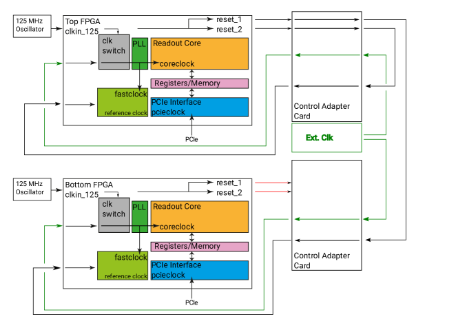
To synchronize the data streams and time stamps from all sensors in the system, a synchronous clock running at is used. Due to the limited number of differential in- and outputs at the used FPGA development board (Altera Stratix IV development kit), the core clock for the FPGAs is applied externally, see figure 2. A switch on the FPGA is used to switch between the external clock and the internal oscillator. A PLL on the FPGA locks to the selected clock and distributes this clock to all connected MuPix sensors. Incoming signals from the tiles are sampled with a counter derived from the selected clock. To synchronize the counters a common synchronous reset signal is used. This signal is created on the master FPGA. A loopback and a differential reset signal to the slave FPGA guarantee a synchronous reset of all counters.
Mechanical Setup
The mechanics are based on optomechanical components from Thorlabs™, providing a
stable and easy-to-use base system.
Two parallel rails, allowing for adjustments along the beam axis and a rotational stage for one
plane allow for flexible positioning of the sensors.
A fully custom, aluminium Printed Circuit Board (PCB) holder mounted on movable posts on the rails allows for
fine sensor adjustments perpendicular to the beam axis with a precision of .
This precision is needed to correct for small sensor placing variations between
different PCBs and therefore maximize the in beam overlap of the sensors.
The same holder system carries the PCBs for the tiles and provides mechanical stability for
the complete system.
The Mupix chips are directly glued to a PCB, which is thinned to underneath the chip to reduce scattering effects at test beams.
The resulting total radiation length is approximately X0 per layer, assuming of glue.
3 High Voltage Monolithic Active Pixel Sensors
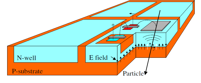
High Voltage Monolithic Active Pixel Sensors [3] are produced in a commercial HV-CMOS process. They allow for direct circuit implants into the pixel matrix. Applying a high voltage of up to between the n-wells and the p-substrate creates a thin depletion zone of about , see figure 3. In the depletion zone, ionizing particles create electron-hole pairs, which drift to the electrodes and create a fast charge signal, which is amplified in the pixel cell. The thin active depletion zone allows for removal of the inactive bulk material. Thinning of the sensors down to leads to a material budget of X0. The signal processing, i.e. discrimination and digitization is implemented in a small inactive part at the edge of the sensor. No further readout ASIC is needed which reduces complexity and costs of the pixel detector.
MuPix7 Prototype
The pixel sensor used in the MuPix telescope is the MuPix7 prototype [4]. It consists of a pixel matrix with a pixel size of . The total active area is . Each pixel cell features an integrated amplifier and has a point to point connection to its partner cell in the periphery of the sensor. In each digital cell, the signal is compared to a threshold, which can be fine-adjusted with tune digital to analog converters (TDACs) for each pixel. The cell address and an 8bit time stamp, running at are stored. An integrated finite state machine performs a priority readout of the hits and sends them 8bit/10bit encoded over a 1.25 GBit/s serial link to the readout FPGA.
4 DAQ System
The DAQ system is designed to run on a single computer with powerful GPU and
CPU (i7-3930K @ , GeForce GTX 680).
The sensor control and readout are steered over two FPGA boards, which are
connected to the computer via the PCIe bus.
Each FPGA controls and receives data from four MuPix7 sensors and is able to receive signals from the scintillating tiles.
The FPGAs can be controlled via a graphical user interface (GUI) on the computer.
The GUI also provides access to the data quality checker and online tracking
results.
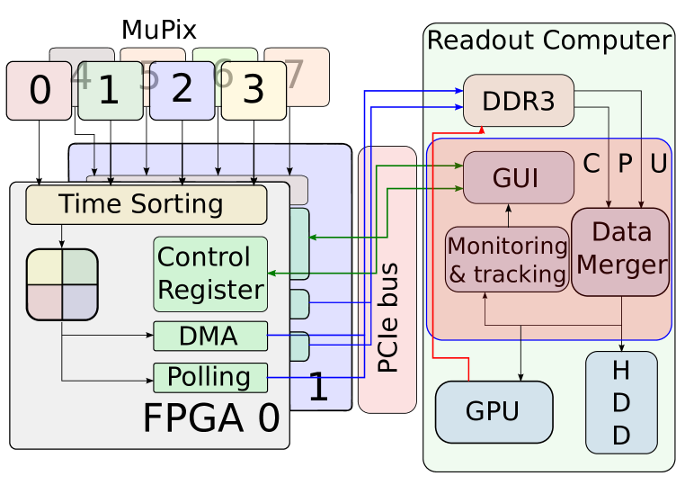
A block diagram of the data flow is shown in figure 4.
The incoming serial hit data from the four sensors is decoded online.
Consequently, a sensor label is assigned to each hit and the four data streams
are merged, sorted by their time stamps and assigned to blocks with 32 time stamps each.
In parallel, blocks with tile signals are created.
The blocks are copied to the local memory of the computer.
The data transfer from the FPGA to the PC was first realized using polling, where the
CPU requests data from the FPGA.
This introduces large overhead and delay in the copying
process.
Therefore, fast direct memory access (DMA) is also implemented for operation at very high rates.
Using DMA, the system bottleneck is the disk writing speed, while in the
polling mode, the polling request overhead limits the readout speed.
Using polling, a track rate of 1 MHz is achieved without errors.
For the DMA, no rate limit is determined up to now.
The theoretical limit is high enough to transfer the data from eight MuPix7
sensors at full rate of approximatly per sensor.
The received data from the two FPGAs is merged into a common data stream and
written to disk.
The data, which is kept in the RAM of the computer is queued to a data quality
checker, which executes online monitoring tasks.
The time stamp distributions, hit maps, time and spatial correlation plots provide
control over the system performance, ensuring timely feedback and high efficiency in test beam
measurements.
The sensor efficiencies and noise rates are also directly computed and
displayed.
Data frames with a potential track, i. e. hits in all layers are further queued
to an online tracking thread, which returns tracking residuals. They are also displayed in the GUI.
This allows for quick alignment and continuous performance control.
To test the performance of the GPU online tracking, the data can be
copied to the GPU, which performs the same tracking operations as the CPU.
Only the residuals for the calculated tracks are returned. It was found, that
the GPU tracking provides exactly
the results as expected [5].
In addition, online tracking performance tests with DMA from the FPGA to the
RAM and then to the GPU have been successfully
performed.
For the online track reconstruction, a straight line fit is implemented. It can be
analytically solved and does not require any iterative procedure.
This makes the fit very fast and robust.
It also has the advantage that the number of calculations is known
and the workload on the GPU can be optimized.
5 Testbeam Results
Several telescopes have been used at DESY ( e+), PSI ( p+, , e+), MAMI ( e+) and CERN ( ) test beam campaigns. The rates varied from several kHz to . The telescope performed well at the different beam conditions. The DAQ system handled track rates of up to 1 MHz and was used as a crucial tool for MuPix characterization measurements.
Alignment and Stability
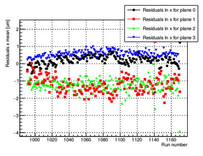
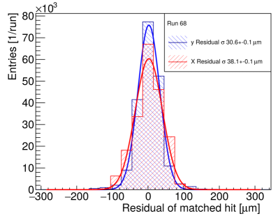
The mechanical alignment precision is of the order of and corrected offline via automated track based alignment to less than , see figure 5. The variation of the mean value of the residuals stays below during the displayed time period of 10 hours. This proves the mechanical stability. The MuPix7 spatial resolution, measured with the MuPix telescope is shown in figure 5 and follows the expected behavior. The spatial resolution is given by the combination of the limited pixel size and the scattering on the planes, which is not included in the fit. For the analyzed run the layer spacing is approximately and the sensors are not rotated. Possible unintended rotations are not taken into account for the alignment. The slight difference of the residual width between x and y resolution is caused by the different dimensions of the pixels ().
Efficiency, Noise and Time Resolution
MuPix7 prototypes were tested at the DESY test beam using settings corresponding to a power
consumption per area of .
For track matching a circular search window of around the
extrapolated track intersection and a time window of around
the track time is chosen.
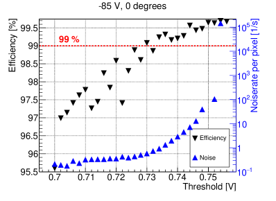
An efficiency above is reached for perpendicular tracks
at a threshold of , while the noise stays below the noise per pixel limit up to
, see figure 6.
Therefore, a threshold operation range of can be used.
This can be improved by rotating the sensor, which increases the particles’
path in the depletion zone.
The higher charge deposit leads to a larger signal and better performance.
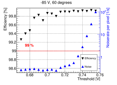
A sensor rotated by shows a threshold operation
range from , see figure 6.
A similar increase in signal size as for the tilt can be achieved by using a substrate with higher
resistivity, which is planned for the upcoming chip submission.
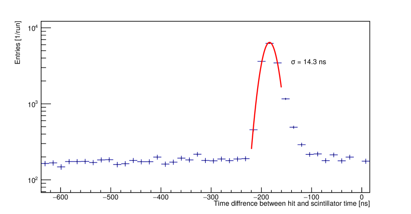
The time resolution of the MuPix7 is studied using the tile scintillators as
precise reference. Events with one track and one tile signal are selected. The
resulting time resolution averaged over all pixels is , expressed as Gaussian , see figure 7.
6 Conclusion and Outlook
The MuPix telescope is used for MuPix sensor characterization and
provides a perfect framework for the development of the Mu3e pixel detector.
The telescope was successfully operated at different beam environments. The
highest useful particle rate is of the order of 1 MHz running the full readout chain.
The MuPix telescope is used to show that the MuPix7 fulfils all performance
goals, required for a successfull operation of the Mu3e detector: Efficiencies
above at moderate noise rates below per pixel and time resolution of .
The estimated power consumption for these measurements is .
The MuPix telescope will be equipped with the new MuPix8 prototype and further used
to characterize the sensors.
Acknowledgements
N. Berger, Q. Huang, A. Kozlinskiy, D. vom Bruch and F. Wauters
thank the Deutsche Forschungsgemeinschaft for supporting them and the
Mu3e project through an Emmy Noether grant.
S. Dittmeier and L. Huth acknowledge support by the IMPRS-PTFS.
A.-K. Perrevoort acknowledges support by the Particle Physics beyond the
Standard Model research training group [GRK 1940].
H. Augustin acknowledges support by the HighRR research training group [GRK
2058].
N. Berger and A. Kozlinskiy thank the PRISMA Cluster of Excellence for
support.
The measurements leading to these results have been performed at the Test Beam
Facility at DESY Hamburg (Germany), a member of the Helmholtz Association
(HGF).
We thank the Institut für Kernphysik at the Johannes Gutenberg University
Mainz for giving us the opportunity to take data at the MAMI beam.
We would like to thank PSI for valuable test beam time.
We owe our SPS test beam time to the SPS team and our LHCb colleagues,
especially Heinrich Schindler, Kazu Akiba and Martin van Beuzekom.
References
- [1] A. Blondel et al. Research Proposal for an Experiment to Search for the Decay . January 2013.
- [2] L. Huth. Development of a Tracking Telescope for Low Momentum Particles and High Rates consisting of HV-MAPS. Master thesis, Physics Institute Heidelberg University, 2014.
- [3] I. Perić. A novel monolithic pixelated particle detector implemented in high-voltage CMOS technology. Nucl.Instrum.Meth., A582:876, 2007.
- [4] H. Augustin et al. The MuPix System-on-Chip for the Mu3e Experiment. In Nuclear Instruments & Methods in Physics Research A (2016), 2016.
- [5] C. Grzesik. Online track reconstruction on graphics processing units for the mupix-telescope. Master thesis, Physics Institute Heidelberg University, 2016.