Quasiballistic quantum transport through Ge/Si core/shell nanowires
Abstract
We study signatures of ballistic quantum transport of holes through Ge/Si core/shell nanowires at low temperatures. We observe Fabry-Prot interference patterns as well as conductance plateaus at integer multiples of 2e2/h at zero magnetic field. Magnetic field evolution of these plateaus reveals relatively large effective Land g-factors. Ballistic effects are observed in nanowires with silicon shell thicknesses of 1 - 3 nm, but not in bare germanium wires. These findings inform the future development of spin and topological quantum devices which rely on ballistic subband-resolved transport.
1 Introduction
A surge of interest in devices based on nanowires with strong spin-orbit interaction is due to their relevance for quantum computing [1, 2, 3, 4, 5, 6, 7] and for the realization of topological superconductivity and Majorana fermions [8, 9]. In this context, spin-orbit interaction in germanium/silicon nanowires was predicted and estimated experimentally to be strong [10, 11, 12, 13, 14, 15], superconducting contacts to these nanowires were demonstrated [16, 17], and large Land g-factors were reported [18, 14]. Moreover, mobility upto 4200 cm2/Vs was reported in these nanowires [19]. These effects, provided they are observed in the ballistic transport regime [20, 21, 22], are essential for Majorana experiments.
In this paper, we report transconductance resonances consistent with one-dimensional (1D) subbands occupied one-by-one as the top gate voltage is made more negative. At low temperatures (1 K) transport is strongly dominated by Fabry-Prot interference patterns. The magnetic field evolution of conductance resonances reveals large g-factors. These effects are observed for a range of silicon shell thicknesses without any obvious dependence on shell thickness of silicon shell thickness, however devices without any shell did not show ballistic transport signatures and exhibited substantial charge instabilities. We estimate the subband spacing to be 20 meV, the low temperature mobility of up to 1000 cm2/Vs and the mean free path of 70 nm. The mean free path is larger than the core diameter consistent with the quasiballistic regime.
2 Fabrication
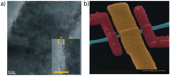
Ge/Si core/shell nanowires (NWs) are grown using the low pressure, cold-walled chemical vapor deposition. NWs are grown with various core diameters (15 - 55 nm) and shell thicknesses (0 - 4 nm) [23]. Fig. 1a shows a high resolution transmission electron micrograph of a Ge/Si core/shell NW demonstrating a high degree of control over the silicon shell thickness [24, 25, 26]. To fabricate devices, the NWs are sonicated in isopropanol and then dropped onto Si3N4 substrates with alignment markers. In order to achieve the low ohmic contact resistance, a dip in hydrofluoric acid is performed to etch the native oxide on the silicon shell. Electron beam evaporation and electron beam lithography are used to define two 150 nm thick nickel contacts. This step is followed by a 30 second rapid thermal annealing at 300∘C. During annealing, Ni diffuses into the NW from both ends forming highly doped NiGex/NiSiy ohmic contacts [27, 28, 29]. Segments of the NW between the sections of NiGex/NiSiy define the Ge/Si channel length (L = 250 - 450 nm). As a last step, a top gate stack consisting of a 10 nm thick hafnium oxide gate dielectric is deposited using atomic layer deposition and then a 30 nm/100 nm thick Ti/Au top gate electrode is evaporated. Gate contact overlaps with the NiGex/NiSiy region fully covering the unannealed Ge/Si channel.

3 Singatures of conductance quantization
Electrical characterization is performed in a dilution refrigerator equipped with a 9 T magnet, using a standard lock-in technique at 27 Hz with an excitation voltage of 50 V. Noise attenuation is done in 2 stages: at room temperature using -filters, and at low temperatures using two-stage low-pass RC filters. Room temperature characterization of the same devices is reported by Nguyen et al.[23]. The room temperature saturation resistance, which is the two-terminal resistance measured at highly negative top gate voltages (Vg), is in the range of 10 k. The room temperature field effect mobility is 150 - 250 cm2/Vs for NWs with silicon shells independent of shell thickness, and 50 cm2/Vs for bare Ge NWs. Measurements in this work show that at low temperatures the saturation resistance is comparable to the room temperature resistance (1 - 20 k). The low temperature field-effect mobility is in the range of 200 - 500 cm2/Vs with the highest mobility of 1000 cm2/Vs extracted from the pinch-off traces using gate-to-nanowire capacitance calculated by a self-consistent Poisson solver (see supplementary information).

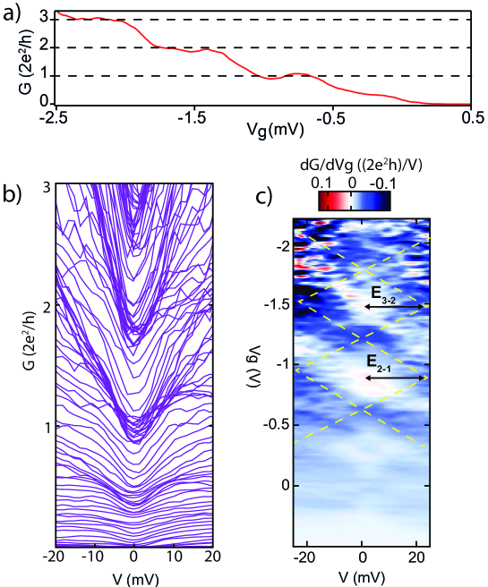
As gate voltage is swept from positive to negative, conductance increases in steps of 2e2/h (Fig. 2a). We associate this with one-dimensional spin-degenerate subband-resolved transport. Additionally, we observe a conductance plateau below the first 2e2/h plateau. Such features are frequently reported in quantum point contacts [30, 31, 32, 33] and are not the focus of the this work. We further investigate this device in the non-linear regime where conductance through the NW is studied as a function of bias voltage (V) and gate voltage. Fig. 2b shows the waterfall plot in which we observe accumulations of conductance traces near 2e2/h and 4e2/h. However, plateaus at 0.5 x 2e2/h that are expected in quantum point contacts at high bias, when the bias exceeds the subband spacing, could not be resolved due to strong current fluctuations at high bias.
Fig. 2c shows the transconductance (dG/dVg) of the data in the panel 2b. High transconductance resonances move linearly as a function of Vg and V. The difference in bias between points where positive and negative slope transconductance resonances meet (forming diamond-shaped regions) indicate the energy separation between the 1D subbands. From Fig. 2c, we observe that the first (E2-1) and second (E3-2) transconductance diamonds have approximately the same size of 22 meV. This energy separation is consistent with transverse quantization in the nanowire for heavy holes with an effective mass of , where is the free electron mass. Additionally, the slopes of the transconductance resonances are used to extract the gate lever arm parameter = dV/dVg = 29.5 meV/V.
4 Magnetotransport

for field oriented at an angle of 45∘ to the nanowire. Black dashed lines mark the spin splitting of the first ( E1 ↑) and second conductance step (E2↓ and E2↑) and green dashed lines mark spin splitting of the third conductance step (E3↓ and E3↑).
Fig. 3 shows the evolution of conductance steps as a function of magnetic field. We note that we only observe Zeeman splitting for the second and third conductance steps while the first step only exhibits a Zeeman shift rather than a splitting. In addition, there are other resonances in fig. 3 which move linearly with magnetic field. We associate these resonances to quantum interference effects [34], similar g-factors can be extracted for these resonances. Zeeman splitting is given by Ez = g B, where is the Bohr’s magneton. We use the lever arm parameter calculated from the transconductance diamond in Fig. 2c to convert the Vg axis into the energy scale. This gives a g-factor for each transition which we denote by g1=2 for the first transition, g2=10.7 2.3 for transition between the first and the second conductance steps and g3=4.7 1.3 for transition between the second and the third conductance step.
Due to the large effective hole masses, the orbital effects of magnetic field are ignored when extracting g-factors, however they may contribute to the shifts of resonances in magnetic field, especially for the resonances with the smaller apparent g-factors. Large g-factors were also recently observed in Ge/Si nanowire quantum dots [18, 14].
5 Fabry-Prot interference
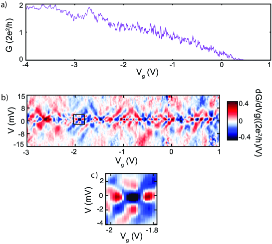
While all devices are fabricated following the same process, of 45 measured devices, only two show signatures of conductance quantization (shown in fig.2 and S1). In a typical device, subband-resolved transport and conductance plateaux are scrambled due to backscattering and are replaced with Fabry-Perot interference within the channel (Fig. 4a). This device is based on a NW with diameter d = 35 nm, length L = 350 nm and shell thickness tsi = 1 nm at T = 400 mK. Mobility extracted from G(Vg) trace at T = 4 K is 450 cm2/Vs. While this trace does not show conductance plateaus, it is a representative trace for many core/shell devices studied at temperatures below 1 K. With the application of negative gate voltage, conductance reaches 4e2/h indicating transport through at least two subbands. In the whole Vg range shown in Fig. 4a, conductance trace exhibits quasi-periodic oscillations. The smallest period measured in Vg is approximately Vg 9 mV. Fig. 4b shows the evolution of these quasi-periodic conductance oscillations as a function of Vg and V: the zero-bias features evolve into checkerboard patterns at finite bias. We attribute this to Fabry-Prot interference [35, 22]. The energy spacing of Fabry-Prot resonances E = 1 - 2 meV (fig.4c) is linked to the cavity length by: E = 75-110 nm. This implies that the segment of NW over which Fabry-Prot interference takes place is approximately one-third of the NW channel.

To conclude, signatures compatible with conductance quantization are measured in Ge/Si NW devices. Magnetic field dependence reveals that the hole g-factor in our NWs is large and exhibits strong anisotropy. Moreover, the presence of a silicon shell on the NW results in quasiballistic transport which is absent in bare Ge NW (see supplementary).
6 Acknowledgement
The Ge/Si nanowire growth was performed at the Center for Integrated Nanotechnologies (CINT), U.S. Department of Energy, Office of Basic Energy Sciences User Facility at Los Alamos National Laboratory (Contract DE-AC52-06NA25396) and Sandia National Laboratories (Contract DE-AC04-94AL85000). We thank Z. Su and A. Zarassi for technical help and useful discussions. S.A.D. acknowledges NSF support under DMR-1503595 and ECCS-1351980. S.M.F. acknowledges NSF DMR-125296, ONR N00014-16-1-2270 and Nanoscience Foundation, Grenoble.
7 References
References
- [1] Nadj-Perge S, Frolov S M, Bakkers E P A M and Kouwenhoven L P 2010 Nature 468 1084–1087 ISSN 0028-0836 URL http://dx.doi.org/10.1038/nature09682
- [2] Pribiag V S, Nadj-Perge S, Frolov S M, van den Berg J W G, van Weperen I, Plissard R, Bakkers M P A and Kouwenhoven L 2013 Nat Nano 8 170–174 ISSN 1748-3387 URL http://dx.doi.org/10.1038/nnano.2013.5
- [3] Veldhorst M, Yang C H, Hwang J C C, Huang W, Dehollain J P, Muhonen J T, Simmons S, Laucht A, Hudson F E, Itoh K M, Morello A and Dzurak A S 2015 Nature 526 410–414 ISSN 0028-0836 URL http://dx.doi.org/10.1038/nature15263
- [4] Patil D K, Corna A, Maurand R, Crippa A, Orlov A, Barraud S, Jehl X, De Franceschi S and Sanquer M 2016 arXiv preprint arXiv:1606.05855
- [5] Maurand R, Jehl X, Patil D K, Corna A, Bohuslavskyi H, Laviéville R, Hutin L, Barraud S, Vinet M, Sanquer M and De Franceschi S 2016 arXiv preprint arXiv:1605.07599
- [6] Bohuslavskyi H, Kotekar-Patil D, Maurand R, Corna A, Barraud S, Bourdet L, Hutin L, Niquet Y M, Jehl X, De Franceschi S, Vinet M and Sanquer M 2016 Applied Physics Letters 109 193101 URL http://scitation.aip.org/content/aip/journal/apl/109/19/10.1063/1.4966946
- [7] Higginbotham A P, Larsen T W, Yao J, Yan H, Lieber C M, Marcus C M and Kuemmeth F 2014 Nano Letters 14 3582–3586 pMID: 24797219 (Preprint http://dx.doi.org/10.1021/nl501242b) URL http://dx.doi.org/10.1021/nl501242b
- [8] Mourik V, Zuo K, Frolov S M, Plissard S R, Bakkers E P A M and Kouwenhoven L P 2012 Science 336 1003–1007 ISSN 0036-8075 (Preprint http://science.sciencemag.org/content/336/6084/1003.full.pdf) URL http://science.sciencemag.org/content/336/6084/1003
- [9] Albrecht S M, Higginbotham A P, Madsen M, Kuemmeth F, Jespersen T S, Nygard J, Krogstrup P and Marcus C M 2016 Nature 531 206–209 ISSN 0028-0836 URL http://dx.doi.org/10.1038/nature17162
- [10] Kloeffel C, Trif M and Loss D 2011 Phys. Rev. B 84(19) 195314 URL http://link.aps.org/doi/10.1103/PhysRevB.84.195314
- [11] Hu Y, Churchill H O H, Reilly D J, Xiang J, Lieber C M and Marcus C M 2007 Nat Nano 2 622–625 ISSN 1748-3387 URL http://dx.doi.org/10.1038/nnano.2007.302
- [12] Hao X J, Tu T, Cao G, Zhou C, Li H O, Guo G C, Fung W Y, Ji Z, Guo G P and Lu W 2010 Nano Letters 10 2956–2960 pMID: 20698609 (Preprint http://dx.doi.org/10.1021/nl101181e) URL http://dx.doi.org/10.1021/nl101181e
- [13] Brauns M, Ridderbos J, Li A, Bakkers E P A M, van der Wiel W G and Zwanenburg F A 2016 Phys. Rev. B 94(4) 041411 URL http://link.aps.org/doi/10.1103/PhysRevB.94.041411
- [14] Zarassi A, Su Z, Danon J, Schwenderling J, Hocevar M, Nguyen B M, Yoo J, Dayeh S A and Frolov S M 2016 ArXiv e-prints (Preprint 1610.04596)
- [15] Maier F, Klinovaja J and Loss D 2014 Phys. Rev. B 90(19) 195421 URL http://link.aps.org/doi/10.1103/PhysRevB.90.195421
- [16] Xiang J, VidanA, TinkhamM, M W and Lieber C M 2006 Nat Nano 1 208–213
- [17] Su Z, Zarassi A, Nguyen B M, Yoo J, Dayeh S A and Frolov S M 2016 ArXiv e-prints (Preprint 1610.03010)
- [18] Brauns M, Ridderbos J, Li A, Bakkers E P A M and Zwanenburg F A 2016 Phys. Rev. B 93(12) 121408 URL http://link.aps.org/doi/10.1103/PhysRevB.93.121408
- [19] Conesa-Boj S, Li A, Koelling S, Brauns M, Ridderbos J, Nguyen T T, Verheijen M A, Koenraad P M, Zwanenburg F A and Bakkers E P A M 2017 Nano Letters 17 2259–2264 pMID: 28231017 (Preprint http://dx.doi.org/10.1021/acs.nanolett.6b04891) URL http://dx.doi.org/10.1021/acs.nanolett.6b04891
- [20] van Weperen I, Plissard S R, Bakkers E P A M, Frolov S M and Kouwenhoven L P 2013 Nano Letters 13 387–391 pMID: 23259576 (Preprint http://dx.doi.org/10.1021/nl3035256) URL http://dx.doi.org/10.1021/nl3035256
- [21] Lu W, Xiang J, Timko B P, Wu Y and Lieber C M 2005 Proceedings of the National Academy of Sciences of the United States of America 102 10046–10051 (Preprint http://www.pnas.org/content/102/29/10046.full.pdf) URL http://www.pnas.org/content/102/29/10046.abstract
- [22] Kretinin A V, Popovitz-Biro R, Mahalu D and Shtrikman H 2010 Nano Letters 10 3439–3445 pMID: 20695446 (Preprint http://dx.doi.org/10.1021/nl101522j) URL http://dx.doi.org/10.1021/nl101522j
- [23] Nguyen B M, Taur Y, Picraux S T and Dayeh S A 2014 Nano Letters 14 585–591 pMID: 24382113 (Preprint http://dx.doi.org/10.1021/nl4037559) URL http://dx.doi.org/10.1021/nl4037559
- [24] Dayeh S A, Gin A V and Picraux S T 2011 Applied Physics Letters 98 163112 URL http://scitation.aip.org/content/aip/journal/apl/98/16/10.1063/1.3574537
- [25] Dayeh S A, Mack N H, Huang J Y and Picraux S T 2011 Applied Physics Letters 99 023102 URL http://scitation.aip.org/content/aip/journal/apl/99/2/10.1063/1.3567932
- [26] Dayeh S A, Tang W, Boioli F, Kavanagh K L, Zheng H, Wang J, Mack N H, Swadener G, Huang J Y, Miglio L, Tu K N and Picraux S T 2013 Nano Letters 13 1869–1876 pMID: 23030346 (Preprint http://dx.doi.org/10.1021/nl3022434) URL http://dx.doi.org/10.1021/nl3022434
- [27] Wu Y, Xiang J, Yang C, Lu W and Lieber C M 2004 Nature 430 61–65 ISSN 0028-0836 URL http://dx.doi.org/10.1038/nature02674
- [28] Tang W, Nguyen B M, Chen R and Dayeh S A 2014 Semiconductor Science and Technology 29 054004 URL http://stacks.iop.org/0268-1242/29/i=5/a=054004
- [29] Dayeh S, Tang W, Nguyen B M, Dai X, Liu Y, Hwang Y, Liu X H and Chen R 2013 ECS Transactions 58 115–125 (Preprint http://ecst.ecsdl.org/content/58/7/115.full.pdf+html) URL http://ecst.ecsdl.org/content/58/7/115.abstract
- [30] Thomas K J, Nicholls J T, Simmons M Y, Pepper M, Mace D R and Ritchie D A 1996 Phys. Rev. Lett. 77(1) 135–138 URL http://link.aps.org/doi/10.1103/PhysRevLett.77.135
- [31] Cronenwett S M, Lynch H J, Goldhaber-Gordon D, Kouwenhoven L P, Marcus C M, Hirose K, Wingreen N S and Umansky V 2002 Phys. Rev. Lett. 88(22) 226805 URL http://link.aps.org/doi/10.1103/PhysRevLett.88.226805
- [32] Reilly D J, Buehler T M, O’Brien J L, Hamilton A R, Dzurak A S, Clark R G, Kane B E, Pfeiffer L N and West K W 2002 Phys. Rev. Lett. 89(24) 246801 URL http://link.aps.org/doi/10.1103/PhysRevLett.89.246801
- [33] Komijani Y, Csontos M, Shorubalko I, Ihn T, Ensslin K, Meir Y, Reuter D and Wieck A D 2010 EPL (Europhysics Letters) 91 67010 URL http://stacks.iop.org/0295-5075/91/i=6/a=67010
- [34] Lundeberg M B and Folk J A 2009 Nat Phys 5 894–897 ISSN 1745-2473 URL http://dx.doi.org/10.1038/nphys1421
- [35] Biercuk M J, Mason N, Martin J, Yacoby A and Marcus C M 2005 Phys. Rev. Lett. 94(2) 026801 URL http://link.aps.org/doi/10.1103/PhysRevLett.94.026801