A versatile, inexpensive integrated photonics platform
Abstract
We present an approach to fabrication and packaging of integrated photonic devices that utilizes waveguide and detector layers deposited at near-ambient temperature. All lithography is performed with a 365 nm i-line stepper, facilitating low cost and high scalability. We have shown low-loss SiN waveguides, high- ring resonators, critically coupled ring resonators, 50/50 beam splitters, Mach-Zehnder interferometers (MZIs) and a process-agnostic fiber packaging scheme. We have further explored the utility of this process for applications in nonlinear optics and quantum photonics. We demonstrate spectral tailoring and octave-spanning supercontinuum generation as well as the integration of superconducting nanowire single photon detectors with MZIs and channel-dropping filters. The packaging approach is suitable for operation up to 160 °C as well as below 1 K. The process is well suited for augmentation of existing foundry capabilities or as a stand-alone process.
I Introduction
The first on-chip photonic components were developed in the mid-1980s, and the subsequent three decades have demonstrated exponential growth in the data capacity per die Kish et al. (2011) due to the miniaturization enabled by integrated photonic devices. Photonic integrated circuits are now playing a role in advanced technologies with applications ranging from atmospheric spectroscopy nac (2016) and medical diagnostics Vollmer and Arnold (2008); Jokerst et al. (2009); Washburn, Gunn, and Bailey (2009); Washburn et al. (2010); Chen et al. (2015) to telecommunications Yamada et al. (2014); Doerr (2015), data centers, Kachris and Tomkos (2012); Nikolova et al. (2015) and supercomputers Rumley et al. (2015); Sun et al. (2015). Each of these integrated photonic application spaces opens new possibilites for science and technology.
The chip-scale photonic devices enabling this innovation are manufactured using lithographic techniques developed by the semiconductor industry, and it is the precision, accuracy, and reliability of these fabrication techniques that has enabled the rapid adoption of integrated photonics for myriad applications. However, the broad range of integrated photonic technologies and application spaces makes it more difficult to create a technology roadmap and a foundry process with broad applicability than it has been for electronics.
The American Institute for Manufacturing of Integrated Photonics (AIM Photonics) aim was launched in 2015, moving integrated photonics closer to the foundry model that has been so successful for integrated electronics. AIM Photonics intends to provide multi-project wafer (MPW) runs, enabling start-ups, small businesses, and academics to leverage the established manufacturing infrastructure. However, many application spaces will not be served by the specific fabrication processes developed for the AIM Photonics technology focus areas. This is unavoidable in the near future due to the enormous diversity of applications of integrated photonic devices and systems. For nonlinear optics in the visible and near-infrared, Si is not a desirable waveguiding medium due to high one- and two-photon absorption Moss et al. (2013). For nonlinear optics in the mid-IR, the absorption of a standard buried SiO2 layer is problematic Soref, Emelett, and Buchwald (2006). For quantum-optical applications such as quantum networks, quantum computers, and quantum metrology, high detection efficiency is required, and superconducting detectors are a very desirable option Marsili et al. (2013). Such detectors are not likely to be incorporated into a foundry process in the near term.
In the present work, we show how a variety of alternative application spaces can be served with a simple, low-cost approach to fabrication of integrated photonic devices and systems as well as a simple back-end-of-line (BEOL) approach to fiber packaging. We introduce a modular fabrication process, employing layers of dielectrics, superconductors, metals, and polymers deposited at near-ambient temperatures ( 65 °C). The dielectrics are deposited using plasma-enhanced chemical vapor deposition (PECVD), and the superconductors are deposited with sputtering. Such deposition techniques are compatible with BEOL processing, so these process modules and photonic devices can be straightforwardly integrated with fully processed wafers from other foundries. For BEOL integration with CMOS electronics, deposition temperatures of less than 400 ∘C can meet many process requirements, and several photonic devices have been demonstrated in such a process Lee and Lipson (2013). Room temperature deposited materials Shao et al. (2016) are even more broadly compatible. With this fabrication process, we have demonstrated low-loss passive SiN waveguides and resonators, critically coupled rings, and Mach-Zehnder interferometers (MZIs), dispersion-engineered waveguides and waveguide-device-integrated WSi superconducting-nanowire single-photon detectors (SNSPDs).
II Fabrication and passive devices
While most Si photonics foundry processes to date utilize crystalline Si as a waveguiding layer, deposited amorphous materials offer several advantages such as low-propagation-loss amorphous silicon (a-Si) Zhu, Lo, and Kwong (2010); Takei et al. (2014) as well as SiN waveguides Sacher et al. (2016); Shao et al. (2016), a wide variety of indices of refraction, lower loss and crosstalk in waveguide crossings Sacher et al. (2016), and 3D layering Sacher et al. (2016); Biberman et al. (2011); Sherwood-Droz and Lipson (2011); Bauters et al. (2011). A schematic of the layers used in this process is shown in Fig. 1. The process begins with a handle Si wafer on which 3 m of thermal SiO2 is grown as a bottom cladding layer. Thermal SiO2 could easily be replaced by PECVD SiO2 deposited at 65 °C for compatibility with BEOL processing. Alternatively, the fabrication process could commence with a handle wafer other than oxidized Si such as sapphire, quartz, diamond, or III-V materials. Next, the SiN waveguiding layer is deposited using plasma-enhanced chemical vapor depositionShao et al. (2016) using N2 and SiH4 as precursors (27 and 30 sccm respectively). The plasma is struck at 30 W and cut to 0 W after 10 s. The chamber pressure is 10 mTorr, and the inductively-coupled power is 1000 W. The wafer temperature has been monitored and does not exceed 65 °C. The resulting SiN film has low stress due to high hydrogen content, so films as thick as 900 nm have been deposited with no cracking or delamination. Even with the excess hydrogen, low propagation losses are observed, as will be discussed shortly.

Following the SiN deposition, and without breaking the vacuum of the PECVD chamber, a thin spacer SiO2 layer is deposited as an etch stop for the WSi SNSPD etch. The wafer is removed from the PECVD chamber and transferred to a sputtering chamber where 3.5 nm WSi is deposited followed by a 2 nm amorphous Si layer Marsili et al. (2013). Both of these sputtering steps are performed at ambient temperature. Alignment marks are etched in the stack. The SNSPD layer is next patterned using using 365 nm i-line stepper photolithography to achieve wires as narrow as 250 nm. The SNSPDs are etched using 40 sccm Ar and 1 sccm SF6 to minimize sidewall residue. The photoresist is stripped, and the waveguide layer is patterned, again using the i-line stepper. The SiN waveguides and all photonic devices (rings, beam splitters, grating couplers) are etched using CF4 chemistry.
After patterning of the SNSPDs and waveguides, Au pads with a Ti adhesion layer are deposited to make contacts to the SNSPDs. Subsequently, the entire wafer is clad with 2 m of PECVD SiO2 deposited with the same tool as was used for the SiN waveguiding layer. Following the cladding deposition, vias are etched through this cladding to allow access to the Au pads for wire bonding. The final layers are SU-8 polymer layers used for packaging and will be discussed in more detail in Sec. III. Fig. 1 shows the full layer stackup.
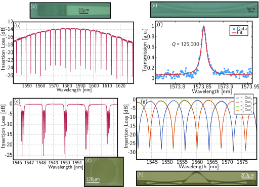
To illustrate the utility of this process, we demonstrate several photonic devices. Figures 2(a) and (b) show microscope images of a SiN grating and the spectral response of a single ring coupled to a waveguide between two gratings. The insertion loss due to the gratings is 6.8 dB/coupler, in close agreement with the finite-difference time-domain simulated value of 6.68 dB/coupler. The 3 dB bandwidth of these couplers is 90 nm. This spectrum was taken after the fibers were fixed in place as described in Sec. III. While the lower index contrast of SiN limits grating efficiency, the insertion loss can be significantly improved with a thicker SiN layer Doerr et al. (2010), a backside mirror Zhang et al. (2014), a second deposited layer Roelkens, Van Thourhout, and Baets (2006), or an additional (partial) etch step Maire et al. (2008). With a backside mirror (which could be integrated easily in this process), insertion loss of 2.6 dB has been demonstrated Zhang et al. (2014), and insertion loss of 2 dB has been simulated Doerr et al. (2010) in a SiN single-etch process similar to this work. The addition of more and higher index layers, such as a-Si, could also improve grating coupler insertion loss. State-of-the-art Si grating couplers have achieved insertion losses of less than 1 dB Mekis et al. (2011); Zaoui et al. (2014), while grating couplers in a two-layer CMOS process with 0.2 dB coupling loss have recently been designed Notaros and Popović (2015). All of these approaches are compatible with the deposited photonics process and packaging approach presented here.
Next we investigated critically coupled ring resonators. In Fig. 2(c) we show the transmission spectrum of four rings coupled to a single bus. One such ring is shown in Fig. 2(d). Each of the four rings has a different gap ranging from 360 nm to 500 nm on the mask, corresponding to 610 nm to 750 nm after fabrication. The optimally coupled device achieved 25 dB extinction across several FSRs. To assess parasitic losses in the critically coupled rings, the most critically coupled resonance from each FSR of the spectrum in Fig. 2(c) was fit to a Lorentzian to obtain a factor. The mean of these resonances was 43,250 (corresponding to an intrinsic of 86,500), and the standard deviation was 2,630.
In addition to critically coupled ring resonators, we have investigated weakly coupled, high- rings. Figure 2(e) shows a microscope image of a ring-bus coupler, and Fig. 2(f) shows a fit to a weakly coupled resonance with -factor of 125,000, corresponding to 2.5 dB/cm propagation loss. The five resonances of this ring closest to 1570 nm were fit to obtain s. The mean of the data set was 110,000 (corresponding to 2.8 dB/cm), and the standard deviation was 8,900. Sidewall roughness due to patterning with i-line lithography is likely the leading contribution to linear propagation losses, as lower losses have been observed in waveguides of similar material when patterned with electron beam lithography (0.8 dB/cm) [Shao et al., 2016] as well as within this process when resist reflow was employed (1.8 dB/cm), as discussed in Sec. IV. This is comparable to PECVD nitride deposited at 400∘C [Lee and Lipson, 2013], but significantly higher than high temperature deposited LPCVD SiN, where losses of less than 0.1 dB/cm have been observed Bauters et al. (2011, 2013); Pfeiffer et al. (2016); Xuan et al. (2016). Silicon waveguides typically exhibit propagation losses near 3 dB/cm [Poon et al., 2015]. Finally, in Fig. 2(g) we show the spectrum of an unbalanced MZI [Fig. 2(h)] demonstrating 25 dB extinction between all ports across 40 nm of spectral bandwidth. This extinction demonstrates that the adiabatic beam splitters created in our process are nearly ideal with no more than 1.5% deviation from 50/50 splitting. If scattered light, noise from the laser source, or unbalanced losses are affecting the visibility, then the beam splitters are even closer to 50/50.
The thermal tuning of passive integrated-photonic devices is often advantageous. A process layer for heaters can be straightforwardly inserted either with evaporated metals or PECVD-deposited and doped a-Si. The a-Si option is particularly attractive due to the decreased electromigration relative to metals, and addition of a-Si to the process is also likely to lead to detectors for high-peak-power pulses used for nonlinear optics.
III Fiber Packaging
Due to the absence of an integrated silicon light source, coupling external light on chip via a robust packaging technique has been an important technological goal for the integrated photonics community. Fiber packaging for operation at cryogenic temperatures is particularly challenging, and many researchers avoid packaging altogether by using fiber positioning stages in the cryostatPernice et al. (2012); Schuck et al. (2016); Sprengers et al. (2011); Najafi et al. (2015). Alternatively, a high-numerical-aperture objective can be used to couple to waveguides through a window in the cryostat Akhlaghi, Schelew, and Young (2015). Such systems typically achieve insertion losses 7 dB, although lower insertion losses have been reported Najafi et al. (2015). Cryogenic coupling with tapered optical fibers has been achieved with losses below 1 dB Srinivasan and Painter (2007). However, coupling with positioning stages requires frequent realignment and high-precision stages inside the cryostat where space is constrained.
The fiber packaging approach presented here is achieved with two processing steps which construct fiber support structures above the grating couplers. These fiber collars comprise two layers of SU-8 epoxy-based photoresist which is permanent upon UV exposure and curing. First, a 20 m pedestal layer is fabricated with SU-8 3020 photoresist. This layer serves to hold an optical fiber at the designed angle relative to the grating (15° in this work). The second SU-8 3050 layer is referred to as the collar, and it is 50 m thick. The collar serves to align the fiber relative to the grating, and it provides a receptacle in which epoxy can be delivered.
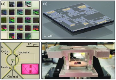
After patterning the SU-8 collar layer, the wafer is diced, and the chips are ready for fiber packaging. A fully processed and diced wafer is shown in Fig. 3(a). It can be seen that multiple die types have been fabricated. A close up of one particular die is shown in Fig. 3(b). The SU-8 pedestal and collar are shown in Fig. 3(c). A grating coupled to a tapered waveguide is also visible, and the inset shows two such fiber collars with a ring coupled to a bus between. In Fig. 3(c) one can see that the fiber collar has two channels on the sides of the fiber. The low viscosity of the epoxy enables it to run through these channels into the ellipse housing the fiber. Upon filling the entire volume, the epoxy is UV-cured. After placing all fibers, an additional amount of epoxy can be delivered to further strengthen the assembly. A fully packaged chip suitable for cryogenic applications is shown in Fig. 3(d).
This packaging approach is suitable for a wide range of operating temperatures. With Dymax OP-4-20632 cryogenic epoxy, we demonstrated cooling of a packaged sample down to 1 K, incurring an additional 1.5 dB insertion loss per coupler. This sample has been thermally cycled twice with the same performance. Additional thermal cycles have not been attempted. With Norland Optical Adhesive, we demonstrated heating up to 160 °C. Upon heating to 120 °C an additional 1 dB insertion loss per coupler was incurred. The sample was held at 120 °C for 16 hours with no additional insertion loss. It was then raised to 160 °C incurring an additional 1 dB insertion loss per coupler. Such packaged chips have been observed to maintain stable coupling for weeks, and the fully encased fibers are protected from the environment to enable exceptional longevity.
We wish to use our waveguide devices to perform spectroscopy in outdoor environments, and also for quantum optical experiments with superconductors in cryogenic environments. Toward these ends, the packaging approach presented here has several strengths. The simplicity renders it useful in many contexts, as it does not depend on KOH wet etch steps to form v-grooves Cohen, Meenehan, and Painter (2013); Beyer et al. (2015), which can be difficult from a process-integration standpoint, and it is not dependent on a two-chip assembly Barwicz and Taira (2014). Alignment of the collar relative to the grating is achieved lithographically, so little optimization is required. Fiber couplers can be placed anywhere on the die for higher density, not just the periphery, as in many v-groove Cohen, Meenehan, and Painter (2013); Beyer et al. (2015) and two-chip approaches Barwicz and Taira (2014). Packaging can be highly automated as the placement of a fiber in a collar and the epoxy delivery is well-suited to robotics with machine vision.
IV Applications in nonlinear optics
SiN waveguides provide an excellent platform for nonlinear optics due to their high nonlinear index (10x larger than silica) Mayer et al. (2015) and low absorption from visible to infrared wavelengths. Recent progress Boggio et al. (2014); Okawachi et al. (2011) has revealed opportunities to use group-velocity-dispersion (GVD) engineered devices in conjunction with high-power ultrafast lasers to generate spectra suitable for applications such as spectroscopy Coddington, Newbury, and Swann (2016), time and frequency metrology Diddams et al. (2000); Hall (2006); Bartels, Heinecke, and Diddams (2009); Diddams (2010), and novel optical sources.
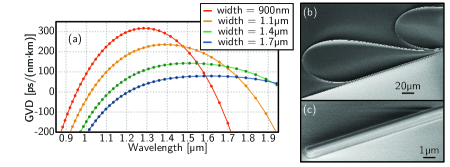
Finite-difference frequency domain calculations show near-zero GVD is achieved for wavelengths in the near-IR by engineering SiN waveguides with thicknesses above 600 nm. For the present study, we investigated waveguides with 700 nm thickness. The GVD curves for these waveguides are shown in Fig. 4(a) for various waveguide widths. These calculations assume thermal SiO2 as an undercladding, air as an overcladding, and employ the SiN index data shown in Fig. 1(b). Waveguides with widths 1.4 m have very flat, near-zero anomalous GVD with one zero crossing at short wavelengths. These waveguides can be used for octave-spanning supercontinuum generation which is useful for self-referenced frequency combs Diddams et al. (2000); Hall (2006); Diddams (2010). Slightly narrower waveguides have anomalous GVD with two zero crossings. As the waveguide width is reduced below 1 m, the anomalous GVD region becomes narrower and drops more steeply to negative values. These waveguides generate narrow, flat-top spectra. Such spectra improve the signal-to-noise ratio for spectroscopic applications targeting a specific narrow frequency band.
Figure 4(b) and (c) show scanning electron micrographs of fabricated waveguides. In addition to the processing described in Sec. II, these waveguides incurred a resist reflow at 150 °C for five minutes before etching. The WSi, SU-8, and overcladding layers were omitted for these devices. Figure 4(b) shows a waveguide in a paperclip configuration Orcutt et al. (2012) to measure propagation losses. These measurements give 1.8 dB/cm propagation loss, an improvement over the loss-ring measurement of the thin waveguides presented in Sec. II (2.5 dB/cm). The loss has not been observed to depend on intensity, indicating that multiphoton absorption is a smaller contribution than sidewall scattering even for femtosecond pulses with 6 kW peak power. Figure 4(c) shows a waveguide with a tapered tip for edge coupling, which was used for these nonlinear optics experiments. Insertion loss of 5.2 dB/facet was measured. For spectroscopy applications in the field or metrology applications in a system, the fiber packaging approach presented in Sec. III can be utilized.
For investigation of nonlinear spectral broadening, a high-power, femtosecond 1550 nm fiber frequency comb with up to 17 kW peak power and 60 fs pulse duration was used as the laser source Sinclair et al. (2015). The source was TE-polarized and coupled into the waveguide tapers with a lensed fiber. Output spectra were recorded as a function of incident power with an optical spectrum analyzer. The measured outputs of 900 nm- and 1900 nm-wide waveguides are presented in Figs. 5(a) and (b), respectively. Also shown on these plots are the theoretical predictions using the GVD curves of Fig. 4(a) in the nonlinear Schrödinger equation (NLSE). The 900 nm device generates a supercontinuum that stays within 20 dB over the wavelength range from 1350 nm to 1850 nm and sharply drops beyond this spectral range. This relatively flat spectrum is suitable for spectroscopy wherein a flat spectrum provides a correspondingly flat response function with a uniform signal-to-noise ratio.

In contrast to the spectrum of Fig. 5(a) the spectrum of Fig. 5(b) shows broad supercontinuum generation from a 2100 nm-wide waveguide. This supercontinuum covers the spectrum from 1050 to 2200 nm when pumped with comb peak power of 5.25 kW. Such a coherent comb spectrum is suitable for self-referenced frequency combs. Additionally, due to the design of the GVD zero crossings at 1.1 m and 2.2 m, the optical power is concentrated at these wavelengths which will be utilized in the difference-frequency generation process.
These examples of spectral tailoring for spectroscopic applications as well as frequency metrology applications show the utility of this deposited-waveguide fabrication process for nonlinear optics.
V Integration with single-photon detectors
For quantum optical applications including metrology, linear-optical quantum computing, and quantum networks, single-photon detection with near-unity efficiency is paramount. For systems utilizing many components, an integrated photonic environment with fiber optics and on-chip devices operating at telecom wavelengths is the most promising route to scaling. Within this context, SNSPDs are a promising candidate for single-photon detection with high efficiency and low timing jitter. The fabrication of SNSPDs on waveguide devices Cavalier et al. (2011); Sprengers et al. (2011); Tanner et al. (2012); Pernice et al. (2012); Atikian et al. (2014); Akhlaghi, Schelew, and Young (2015); Kahl et al. (2015); Beyer et al. (2015); Sahin et al. (2015); Najafi et al. (2015); Schuck et al. (2016) has been described in Sec. II.
The detection mechanism of an SNSPD depends on the absorption of a photon locally breaking Cooper pairs in the superconductor, leading to the production of a region of normal metal, referred to as a “hot spot”. With sufficient bias current, the absorption of a photon by the SNSPD will result in a voltage pulse Gol’tsman et al. (2001a); Natarajan, Tanner, and Hadfield (2012); Liu et al. (2013); Kerman et al. (2009); Jahanmirinejad and Fiore (2012); Casaburi et al. (2015, 2013); Marsili et al. (2009); Divochiy et al. (2008); Yang et al. (2007); Fitch et al. (2003); Marsili et al. (2013). The required wire dimensions for this process depend on the wavelength of the light and the material properties. Typical SNSPD materials are NbN Gol’tsman et al. (2001b) or WSi Baek et al. (2011). WSi devices typically have a lower critical temperature and higher timing jitter than NbN, but at present have higher yield and higher detection efficiency. Here we explore WSi SNSPDs.
For detection of 1550 nm photons, typical WSi wires are 130 nm wide and 4 nm thick Marsili et al. (2013). In wires much wider than this, the hot spot created via photon absorption is not large enough to span the width of the wire and result in a voltage pulse, even when the wire is biased very close to its critical current. However, using the lithographic system available to us, we cannot achieve such narrow features. To circumvent this issue, we experimented with varying the film thickness with the intention of achieving similar photon detection efficiency with wider wires.
We incorporated these SNSPDs into several photonic devices. Figure 6(a) shows an optical micrograph of an MZI with two fiber input ports and WSi SNSPDs at the output ports. Figure 6(b) shows an optical micrograph of the waveguide-integrated SNSPD, and Fig. 6(c) shows a scanning electron micrograph of the photolithographically patterned nanowire with 250 nm width.
The response of a waveguide-integrated WSi SNSPD with 250 nm width and 3.5 nm (85% the typical thickness Marsili et al. (2013)) to light at 1570 nm is shown in Fig. 6(d) for different input powers at the grating. For these measurements, the device was operated at 740 mK. Not only do we find that these wider, thinner wires are capable of detecting photons of this energy, we observe a broad plateau as a function of bias current, indicating saturated internal quantum detection efficiency. We note that thinning of our SNSPD material suppresses the critical temperature and current, leading to reduced performance, limiting the extent to which thinning the material can relax the lithographic requirements. A thorough study of SNSPD performance across the parameter space of width and thickness will be the subject of future work.

The optical transmission spectra from each of the two MZI input ports to each of the two detectors is shown in Fig. 6(e), and nearly 30 dB extinction is observed. The data in Fig. 6(d) was acquired from one of these detectors, and their performance was nearly identical. The minor offset of the spectra along the wavelength axis is due to imprecise timing alignment between the sweep of the laser and the SNSPD data acquisition, resulting in a slight inaccuracy in the recorded wavelength.
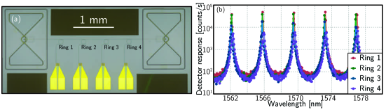
Finally, we integrated the SNSPDs at the drop ports of four first-order filters. An optical micrograph of the optoelectronic devices is shown in Fig. 7(a). The ring design used for this device is the same as that shown in Fig. 2(c), except with a drop port as well as a through port and a 650 nm ring-bus gap on both ports. The detector response as a function of wavelength is shown in Fig. 7(b) for the detectors at all four drop ports. Extinction of 20 dB is observed for all four detectors. We note that the yield of these detectors fabricated from WSi using i-line lithography was quite high, and it was not necessary to test multiple MZI devices or filter banks to find one with all detectors working. Such a fabrication process is scalable to large systems without the need for pick-and-place device assembly methods Najafi et al. (2015).
VI Summary and Outlook
We have presented an approach to fabrication and packaging of integrated photonic devices that utilizes waveguide and detector layers deposited at near-ambient temperature. All lithography was performed with a 365 nm i-line stepper. We have shown low-loss waveguides, high- ring resonators, critically coupled ring resonators, 50/50 beam splitters, MZIs, and a robust fiber-packaging system. We have further explored the utility of this process by demonstrating spectral tailoring and supercontinuum generation of a fiber-generated frequency comb. Finally, we demonstrated the applicability of this fabrication process to quantum-optical systems by integrating SNSPDs with MZIs and channel-dropping filters.
Because all layers in this process are deposited at near-ambient temperature, and because the fiber packaging approach is compatible with a wide variety of substrates, devices, and processes, this fabrication process is compatible with BEOL incorporation on fully processed CMOS wafers or wafers of integrated photonic devices fabricated by other foundries. Additionally, because we have only made use of deposited films for the waveguide and detector layers, it is possible to extend this platform by vertically stacking many layers of waveguides and detectors using interlayer waveguide couplers to construct complex, 3D photonic systems.
Regarding the utility of this scalable and nimble fabrication infrastructure, we note that the cost of all equipment used to perform the fabrication of these devices is quite low. The PECVD tool costs $400K, and can also serve as the RIE tool. The sputtering tool also costs $400K. The i-line stepper is $3.2M. Thus, the entire capital investment for this equipment could be as low as $4M, making this approach accessible for start-ups, small businesses, academics, and innovators in developing countries. If added to an existing foundry, the additional capital investment would be a small fraction of the total cost of the foundry. Based on these results, we are of the opinion that as integrated photonics moves to a foundry process model, innovation per dollar can be maximized through investment in nimble and diverse processes serving a wider range of application spaces.
This is a contribution of NIST, an agency of the US government, not subject to copyright. Product disclaimer: Any mention of commercial products is for information only; it does not imply recommendation or endorsement by NIST.
References
- Kish et al. (2011) F. Kish, D. Welch, R. Nagarajan, J. Pleumeekers, V. Lal, M. Ziari, A. Nilsson, M. Kato, S. Murthy, P. Evans, S. Corzine, M. Mitchell, P. Samra, J. Rahn, M. V. Leeuwen, J. Stewart, D. Lambert, R. Muthiah, H.-S. Tsai, J. Bostak, A. Dentai, K.-T. Wu, H. Sun, D. Pavinski, J. Zhang, J. Tang, J. McNicol, M. Kuntz, V. Dominic, B. Taylor, R. Salvatore, M. Fisher, A. Spannagel, E. Strezelecka, P. Studenkov, M. Raburn, W. Williams, D. Christini, K. T. S. Agashe, R. Malendevich, G. Goldfarb, S. Melle, C. Joyner, M. Kaufman, and S. Grubb, “Current status of large-scale inp photonic integrated circuits,” IEEE J. Sel. Topics Quant. Electron. 17, 1470 (2011).
- nac (2016) Spectral engineering of frequency combs using deposited waveguides (2016).
- Vollmer and Arnold (2008) F. Vollmer and S. Arnold, “Whispering-gallery-mode biosensing: label-free detection down to single molecules,” Nat. Methods 5, 591 (2008).
- Jokerst et al. (2009) N. Jokerst, M. Royal, S. Palit, L. Luan, S. Dhar, and T. Tyler, “Chip scale integrated microresonator sensing systems,” J. Biophotonics 2, 212 (2009).
- Washburn, Gunn, and Bailey (2009) A. Washburn, L. Gunn, and R. Bailey, “Label-free quantitation of a cancer biomarker in complex media using silicon photonic microring resonators,” Anal. Chem. 81, 9499 (2009).
- Washburn et al. (2010) A. Washburn, M. Luchansky, A. Bowman, and R. Bailey, “Quantitative, label-free detection of five protein biomarkers using multiplexed arrays of silicon photonic microring resonators,” Anal. Chem. 82, 69 (2010).
- Chen et al. (2015) Y. Chen, F. Yu, C. Yang, J. Song, L. Tang, M. Li, and J.-J. He, “Label-free biosensing using cascaded double-microring resonators integrated with microfluidic channels,” Opt. Comm. 344, 129 (2015).
- Yamada et al. (2014) K. Yamada, T. Tsuchizawa, H. Nishi, R. Kou, T. Hiraki, K. Takeda, H. Fukuda, Y. Ishikawa, K. Wada, and T. Yamamoto, “High-performance silicon photonics technology for telecommunications applications,” Sci. Technol. Adv. Mater. 15, 024603 (2014).
- Doerr (2015) C. Doerr, “Silicon photonic integration in telecommunications,” Frontiers in Physics 3, 37 (2015).
- Kachris and Tomkos (2012) C. Kachris and I. Tomkos, “A survey on optical interconnects for data centers,” IEEE Comm. Surveys Tutorials 14, 1021 (2012).
- Nikolova et al. (2015) D. Nikolova, S. Rumley, D. Calhoun, A. Li, R. Hendry, P. Samadi, and K. Bergman, “Scaling silicon photonic switch fabrics for data center interconnection networks,” Opt. Express 23, 1159 (2015).
- Rumley et al. (2015) S. Rumley, D. Nikolova, R. Hendry, Q. Li, D. Calhoun, and K. Bergman, “Silicon photonics for exascale systems,” J. Lightwave Tech. 33, 547 (2015).
- Sun et al. (2015) C. Sun, M. Wade, Y. Lee, J. Orcutt, L. Alloatti, M. Georgas, A. Waterman, J. Shainline, R. Avizienis, S. Lin, B. Moss, R. Kumar, F. Pavanello, A. Atabaki, H. Cook, A. Ou, J. Leu, Y.-H. Chen, K. Asanović, R. Ram, M. Popović, and V. Stojanović, “Single-chip microprocessor that communicates directly using light,” Nature 528, 534 (2015).
- (14) “American institute for manufacturing integrated photonics,” .
- Moss et al. (2013) D. J. Moss, R. Morandotti, A. L. Gaeta, and M. Lipson, “New CMOS-compatible platforms based on silicon nitride and Hydex for nonlinear optics,” Nat. Photon. 7, 597–607 (2013).
- Soref, Emelett, and Buchwald (2006) R. A. Soref, S. J. Emelett, and W. R. Buchwald, “Silicon waveguided components for the long-wave infrared region,” Journal of Optics A: Pure and Applied Optics 8, 840–848 (2006).
- Marsili et al. (2013) F. Marsili, V. B. Verma, J. A. Stern, S. Harrington, A. E. Lita, T. Gerrits, I. Vayshenker, B. Baek, M. D. Shaw, R. P. Mirin, and S. W. Nam, “Detecting single infrared photons with 93% system efficiency,” Nat. Photon. 7, 210–214 (2013).
- Lee and Lipson (2013) Y. H. D. Lee and M. Lipson, “Back-End Deposited Silicon Photonics for Monolithic Integration on CMOS,” IEEE Journal of Selected Topics in Quantum Electronics 19, 8200207–8200207 (2013).
- Shao et al. (2016) Z. Shao, Y. Chen, H. Chen, Y. Zhang, F. Zhang, J. Jian, Z. Fan, L. Liu, C. Yang, L. Zhou, and S. Yu, “Ultra-low temperature silicon nitride photonic integration platform,” Opt. Express 24, 1865 (2016).
- Zhu, Lo, and Kwong (2010) S. Zhu, G. Lo, and D. Kwong, “Low-loss amorphous silicon wire waveguide for integrated photonics: effect of fabrication process and the thermal stability,” Opt. Express 18, 25283 (2010).
- Takei et al. (2014) R. Takei, S. Manako, E. Omoda, Y. Sakakibara, M. Mori, and T. Kamei, “Sub-1 db/cm submicrometer-scale amorphous silicon waveguide for backend on-chip optical interconnect,” Opt. Express 22, 4779 (2014).
- Sacher et al. (2016) W. Sacher, Z. Yong, J. Mikkelsen, A. Bois, Y. Yang, J. Mak, P. Dumais, D. Goodwill, C. Ma, J. Jeong, E. Bernier, and J. Poon, “Multilayer silicon nitride-on-silicon integrated photonic platform for 3d photonic circuits,” Conference on Lasers and Electro-optics , JTh4C.3 (2016).
- Biberman et al. (2011) A. Biberman, K. Preston, G. Hendry, N. Sherwood-Droz, J. Chan, J. S. Levy, M. Lipson, and K. Bergman, “Photonic network-on-chip architectures using multilayer deposited silicon materials for high-performance chip multiprocessors,” ACM Journal on Emerging Technologies in Computing Systems 7, 1–25 (2011).
- Sherwood-Droz and Lipson (2011) N. Sherwood-Droz and M. Lipson, “Scalable 3D dense integration of photonics on bulk silicon,” Optics Express 19, 17758 (2011).
- Bauters et al. (2011) J. F. Bauters, M. J. R. Heck, D. John, D. Dai, M.-C. Tien, J. S. Barton, A. Leinse, R. G. Heideman, D. J. Blumenthal, and J. E. Bowers, “Ultra-low-loss high-aspect-ratio Si3N4 waveguides,” Optics Express 19, 3163 (2011).
- Doerr et al. (2010) C. R. Doerr, L. Chen, Y.-K. Chen, and L. L. Buhl, “Wide Bandwidth Silicon Nitride Grating Coupler,” IEEE Photonics Technology Letters 22, 1461–1463 (2010).
- Zhang et al. (2014) H. Zhang, C. Li, X. Tu, H. Zhou, X. Luo, M. Yu, and P. G.-Q. Lo, “High Efficiency Silicon Nitride Grating Coupler with DBR,” in Optical Fiber Communication Conference (OSA, Washington, D.C., 2014) p. Th1A.4.
- Roelkens, Van Thourhout, and Baets (2006) G. Roelkens, D. Van Thourhout, and R. Baets, “High efficiency Silicon-on-Insulator grating coupler based on a poly-Silicon overlay,” Optics Express 14, 11622 (2006).
- Maire et al. (2008) G. Maire, L. Vivien, G. Sattler, A. Kazmierczak, B. Sanchez, K. B. Gylfason, A. Griol, D. Marris-Morini, E. Cassan, D. Giannone, H. Sohlström, and D. Hill, “High efficiency silicon nitride surface grating couplers,” Optics Express 16, 328 (2008).
- Mekis et al. (2011) A. Mekis, S. Gloeckner, G. Masini, A. Narasimha, T. Pinguet, S. Sahni, and P. De Dobbelaere, “A Grating-Coupler-Enabled CMOS Photonics Platform,” IEEE Journal of Selected Topics in Quantum Electronics 17, 597–608 (2011).
- Zaoui et al. (2014) W. S. Zaoui, A. Kunze, W. Vogel, M. Berroth, J. Butschke, F. Letzkus, and J. Burghartz, “Bridging the gap between optical fibers and silicon photonic integrated circuits,” Optics Express 22, 1277 (2014).
- Notaros and Popović (2015) J. Notaros and M. Popović, “Band-Structure Approach to Synthesis of Grating Couplers with Ultra-High Coupling Efficiency and Directivity,” in Optical Fiber Communication Conference (OSA, Washington, D.C., 2015) p. Th3F.2.
- Bauters et al. (2013) J. F. Bauters, M. L. Davenport, M. J. R. Heck, J. K. Doylend, A. Chen, A. W. Fang, and J. E. Bowers, “Silicon on ultra-low-loss waveguide photonic integration platform,” Optics Express 21, 544 (2013).
- Pfeiffer et al. (2016) M. Pfeiffer, A. Kordts, V. Brasch, M. Zervas, M. Geiselmann, J. Jost, and T. Kippenberg, “Photonic damascene process for integrated high-q microresonator based nonlinear photonics,” Optica 3, 20 (2016).
- Xuan et al. (2016) Y. Xuan, Y. Liu, L. Varghese, A. Metcalf, X. Xue, P.-H. Wang, K. Han, J. Jaramillo-Villegas, A. Noman, C. Wang, S. Kim, M. Teng, Y. Lee, B. Niu, L. Fan, J. Wang, D. Leaird, A. Weiner, and M. Qi, “High-q silicon nitride microresonators exhibiting low-power frequency comb initiation,” Optica 3, 1171 (2016).
- Poon et al. (2015) J. K. S. Poon, W. D. Sacher, Y. Huang, and G.-Q. Lo, “Multilayer Silicon Nitride-on-Silicon Integrated Photonic Platforms,” in 2015 IEEE Compound Semiconductor Integrated Circuit Symposium (CSICS) (IEEE, 2015) pp. 1–4.
- Pernice et al. (2012) W. H. P. Pernice, C. Schuck, O. Minaeva, M. Li, G. N. Goltsman, A. V. Sergienko, and H. X. Tang, “High-speed and high-efficiency travelling wave single-photon detectors embedded in nanophotonic circuits.” Nat. Comm. 3, 1325 (2012).
- Schuck et al. (2016) C. Schuck, X. Guo, L. Fan, X. Ma, M. Poot, and H. X. Tang, “Quantum interference in heterogeneous superconducting-photonic circuits on a silicon chip.” Nat. Comm. 7, 10352 (2016).
- Sprengers et al. (2011) J. P. Sprengers, A. Gaggero, D. Sahin, S. Jahanmirinejad, G. Frucci, F. Mattioli, R. Leoni, J. Beetz, M. Lermer, M. Kamp, S. Höfling, R. Sanjines, and A. Fiore, “Waveguide superconducting single-photon detectors for integrated quantum photonic circuits,” Appl. Phys. Lett. 99, 181110 (2011).
- Najafi et al. (2015) F. Najafi, J. Mower, N. C. Harris, F. Bellei, A. Dane, C. Lee, X. Hu, P. Kharel, F. Marsili, S. Assefa, K. K. Berggren, and D. Englund, “On-chip detection of non-classical light by scalable integration of single-photon detectors.” Nat. Comm. 6, 5873 (2015).
- Akhlaghi, Schelew, and Young (2015) M. K. Akhlaghi, E. Schelew, and J. F. Young, “Waveguide integrated superconducting single-photon detectors implemented as near-perfect absorbers of coherent radiation.” Nat. Comm. 6, 8233 (2015).
- Srinivasan and Painter (2007) K. Srinivasan and O. Painter, “Optical fiber taper coupling and high-resolution wavelength tuning of microdisk resonators at cryogenic temperatures,” Appl. Phys. Lett. 90, 031114 (2007).
- Cohen, Meenehan, and Painter (2013) J. D. Cohen, S. M. Meenehan, and O. Painter, “Optical coupling to nanoscale optomechanical cavities for near quantum-limited motion transduction,” Optics Express 21, 11227 (2013).
- Beyer et al. (2015) A. Beyer, R. Briggs, F. Marsili, J. D. Cohen, S. M. Meenehan, O. J. Painter, and M. Shaw, “Waveguide-Coupled Superconducting Nanowire Single-Photon Detectors,” in CLEO: 2015 (OSA, Washington, D.C., 2015) p. STh1I.2.
- Barwicz and Taira (2014) T. Barwicz and Y. Taira, “Low-Cost Interfacing of Fibers to Nanophotonic Waveguides: Design for Fabrication and Assembly Tolerances,” IEEE Photonics Journal 6, 1–18 (2014).
- Mayer et al. (2015) A. S. Mayer, A. Klenner, A. R. Johnson, K. Luke, M. R. E. Lamont, Y. Okawachi, M. Lipson, A. L. Gaeta, and U. Keller, “Frequency comb offset detection using supercontinuum generation is silicon nitride waveguides,” Opt. Express 12, 015440 (2015).
- Boggio et al. (2014) J. M. C. Boggio, D. Bodenmüller, T. Fremberg, R. Haynes, M. M. Roth, R. Eisermann, M. Lisker, L. Zimmermann, and M. Böhm, “Dispersion engineered silicon nitride waveguides by geometrical and refractive-index optimization,” J. Opt. Soc. Am. B 31, 2846 (2014).
- Okawachi et al. (2011) Y. Okawachi, K. Saha, J. S. Levy, Y. H. Wen, M. Lipson, and A. L. Gaeta, “Octave-spanning frequency comb generation in a silicon nitride chip,” Opt. Lett. 36, 3398 (2011).
- Coddington, Newbury, and Swann (2016) I. Coddington, N. Newbury, and W. Swann, “Dual-comb spectroscopy,” Optica 3, 414 (2016).
- Diddams et al. (2000) S. Diddams, D. Jones, J. Ye, S. Cundiff, J. Hall, J. Ranka, R. Windeler, R. Holzwarth, T. Udem, and T. Hänsch, “Direct link between microwave and optical frequencies with a 300 thz femtosecond laser comb,” Phys. Rev. Lett. 84, 5102 (2000).
- Hall (2006) J. Hall, “Defining and measuring optical frequencies,” Rev. Mod. Phys. 78, 1279 (2006).
- Bartels, Heinecke, and Diddams (2009) A. Bartels, D. Heinecke, and S. Diddams, “10-ghz self-referenced optical frequency comb,” Science 326, 681 (2009).
- Diddams (2010) S. Diddams, “The evolving optical frequency comb,” J. Opt. Soc. Am. B 27, B51 (2010).
- Orcutt et al. (2012) J. Orcutt, S. Tang, S. Kramer, K. Mehta, H. Li, , V. Stojanović, and R. Ram, “Low-loss polysilicon waveguides fabricated in an emulated high-volume electronics process,” Opt. Express 20, 7243 (2012).
- Sinclair et al. (2015) L. Sinclair, J.-D. Deschênes, L. Sonderhouse, I. K. W.C. Swann, E. Baumann, N. Newbury, and I. Coddington, “A compact optically coherent fiber frequency comb,” Rev. Sci. Instrum. 86, 081301 (2015).
- Cavalier et al. (2011) P. Cavalier, J.-C. Villégier, P. Feautrier, C. Constancias, and A. Morand, “Light interference detection on-chip by integrated SNSPD counters,” AIP Advances 1, 042120 (2011).
- Tanner et al. (2012) M. G. Tanner, L. S. E. Alvarez, W. Jiang, R. J. Warburton, Z. H. Barber, and R. H. Hadfield, “A superconducting nanowire single photon detector on lithium niobate.” Nanotechnology 23, 505201 (2012).
- Atikian et al. (2014) H. A. Atikian, A. Eftekharian, A. Jafari Salim, M. J. Burek, J. T. Choy, A. Hamed Majedi, and M. Lončar, “Superconducting nanowire single photon detector on diamond,” Appl. Phys. Lett. 104, 122602 (2014).
- Kahl et al. (2015) O. Kahl, S. Ferrari, V. Kovalyuk, G. N. Goltsman, A. Korneev, and W. H. P. Pernice, “Waveguide integrated superconducting single-photon detectors with high internal quantum efficiency at telecom wavelengths.” Scientific reports 5, 10941 (2015).
- Sahin et al. (2015) D. Sahin, A. Gaggero, J.-W. Weber, I. Agafonov, M. A. Verheijen, F. Mattioli, J. Beetz, M. Kamp, S. Hofling, M. C. M. van de Sanden, R. Leoni, and A. Fiore, “Waveguide Nanowire Superconducting Single-Photon Detectors Fabricated on GaAs and the Study of Their Optical Properties,” IEEE Journal of Selected Topics in Quantum Electronics 21, 1–10 (2015).
- Gol’tsman et al. (2001a) G. Gol’tsman, O. Okunev, G. Chulova, A. Lipatov, A. Semenov, K. Smirnov, B. Voronov, A. Dzardanov, C. Williams, and R. Sobolewski, “Picosecond superconducting single-photon optical detector,” Appl. Phys. Lett. 79, 705 (2001a).
- Natarajan, Tanner, and Hadfield (2012) C. Natarajan, M. Tanner, and R. Hadfield, “Superconducting nanowire single-photon detectors: physics and applications,” Supercond. Sci. Tech. 25, 063001 (2012).
- Liu et al. (2013) D. Liu, L. You, S. Chen, X. Yang, Z. Wang, Y. Wang, X. Xie, and M. Jiang, “Electrical characteristics of superconducting nanowire single photon detector,” IEEE Trans. Appl. Supercond. 23, 2200804 (2013).
- Kerman et al. (2009) A. Kerman, J. Yang, R. Molnar, E. Dauler, and K. Berggren, “Electrothermal feedback in superconducting nanowire single-photon detectors,” Phys. Rev. B 79, 100509(R) (2009).
- Jahanmirinejad and Fiore (2012) S. Jahanmirinejad and A. Fiore, “Proposal for a superconducting photon number resolving detector with large dynamic range,” Opt. Express 20, 5017 (2012).
- Casaburi et al. (2015) A. Casaburi, R. Heath, M. Ejrnaes, C. Nappi, R. Cristiano, and R. Hadfield, “Experimental evidence for photoinduced vortex crossing in current carrying superconducting strips,” Phys. Rev. B 92, 214512 (2015).
- Casaburi et al. (2013) A. Casaburi, R. Heath, M. Tanner, R. Cristiano, M. Ejrnaes, C. Nappi, and R. Hadfield, “Current distribution in a parallel configuration superconducting strip-line detector,” Appl. Phys. Lett. 103, 013503 (2013).
- Marsili et al. (2009) F. Marsili, D. Bitauld, A. Gaggero, S. Jahanmirinejad, R. Leoni, F. Mattioli, and A. Fiore, “Physics and application of photon number resolving detectors based on superconducting parallel nanowires,” New J. Phys. 11, 045022 (2009).
- Divochiy et al. (2008) A. Divochiy, F. Marsili, D. Bitauld, A. Gaggero, R. Leoni, F. Mattioli, A. Korneev, V. Seleznev, N. Kaurova, O. Minaeva, G. Gol’tsman, K. Lagoudakis, M. Benkhaoul, F. Lévy, and A. Fiore, “Superconducting nanowire photon-number-resolving detector at telecommunication wavelengths,” Nat. Photon 2, 302 (2008).
- Yang et al. (2007) J. Yang, A. Kerman, E. Dauler, V. Anant, K. Rosfjord, and K. Berggren, “Modeling the electrical and thermal response of superconducting nanowire single-photon detectors,” IEEE Trans. Appl. Supercond. 17, 581 (2007).
- Fitch et al. (2003) M. Fitch, B. Jacobs, T. Pittman, and J. Franson, “Photon-number resolution using time-multiplexed single-photon detectors,” Phys. Rev. A 68, 043814 (2003).
- Gol’tsman et al. (2001b) G. N. Gol’tsman, O. Okunev, G. Chulkova, A. Lipatov, A. Semenov, K. Smirnov, B. Voronov, A. Dzardanov, C. Williams, and R. Sobolewski, “Picosecond superconducting single-photon optical detector,” Appl. Phys. Lett. 79, 705 (2001b).
- Baek et al. (2011) B. Baek, A. E. Lita, V. Verma, and S. W. Nam, “Superconducting a-WxSi1-x nanowire single-photon detector with saturated internal quantum efficiency from visible to 1850 nm,” Appl. Phys. Lett. 98, 251105 (2011).