Weak ferromagnetism and short range polar order in NaMnF3 thin films
Abstract
The orthorhombically distorted perovskite NaMnF3 has been predicted to become ferroelectric if an distortion of the bulk Pnma structure is imposed. In order to test this prediction, NaMnF3 thin films were grown on SrTiO3 (001) single crystal substrates via molecular beam epitaxy. The best films were smooth and single phase with four different twin domains. In-plane magnetization measurements revealed the presence of antiferromagnetic ordering with weak ferromagnetism below the Néel temperature K. For the dielectric studies, NaMnF3 films were grown on a 30 nm SrRuO3 (001) layer used as a bottom electrode grown via pulsed laser deposition. The complex permittivity as a function of frequency indicated a strong Debye-like relaxation contribution characterized by a distribution of relaxation times. A power-law divergence of the characteristic relaxation time revealed an order-disorder phase transition at 8 K. The slow relaxation dynamics indicated the formation of super-dipoles (superparaelectric moments) that extend over several unit cells, similar to polar nanoregions of relaxor ferroelectrics.
There is much interest in multiferroic (MF) materials that show coexistence of two or more long-range orders such as ferroelectricity, (anti-) ferromagnetism and/or ferroelasticity. Magnetoelectric (ME) coupling can allow for the control of magnetization (electric polarization ) using an electric field (a magnetic field ), which can be used for potential applications in data storage, sensors and spintronic devices. Eerenstein, Mathur, and Scott (2006); Fiebig (2005); Cherepov et al. (2014); Cheong and Mostovoy (2007); Hayes et al. (2016) As a result, there has been much effort expended towards synthesizing MF insulating materials with strong ME coupling at room temperature.Zhao et al. (2006); Park et al. (2007); Yang et al. (2016); Hwang et al. (2015)
Many MF materials are oxides, but multiferroicity can also be found in fluorides. For example, in the orthorhombic BaF4 family the Co and Ni compounds in bulk form are ferroelectric (FE) and antiferromagnetic.Scott and Blinc (2011) While in oxide perovskites ABO3 the simultaneous presence of FE and magnetic orderings is limited by conflicting requirements for the electronic configuration of the transition metal in the B-site,Cohen (1992) ferroelectricity in BaMnF4 is mainly due to geometric (topological) reasons.Ravez (2000) Recent experiments showed that BaCoF4 thin films are weakly ferromagnetic at low temperatures due to strain.Borisov et al. (2016)
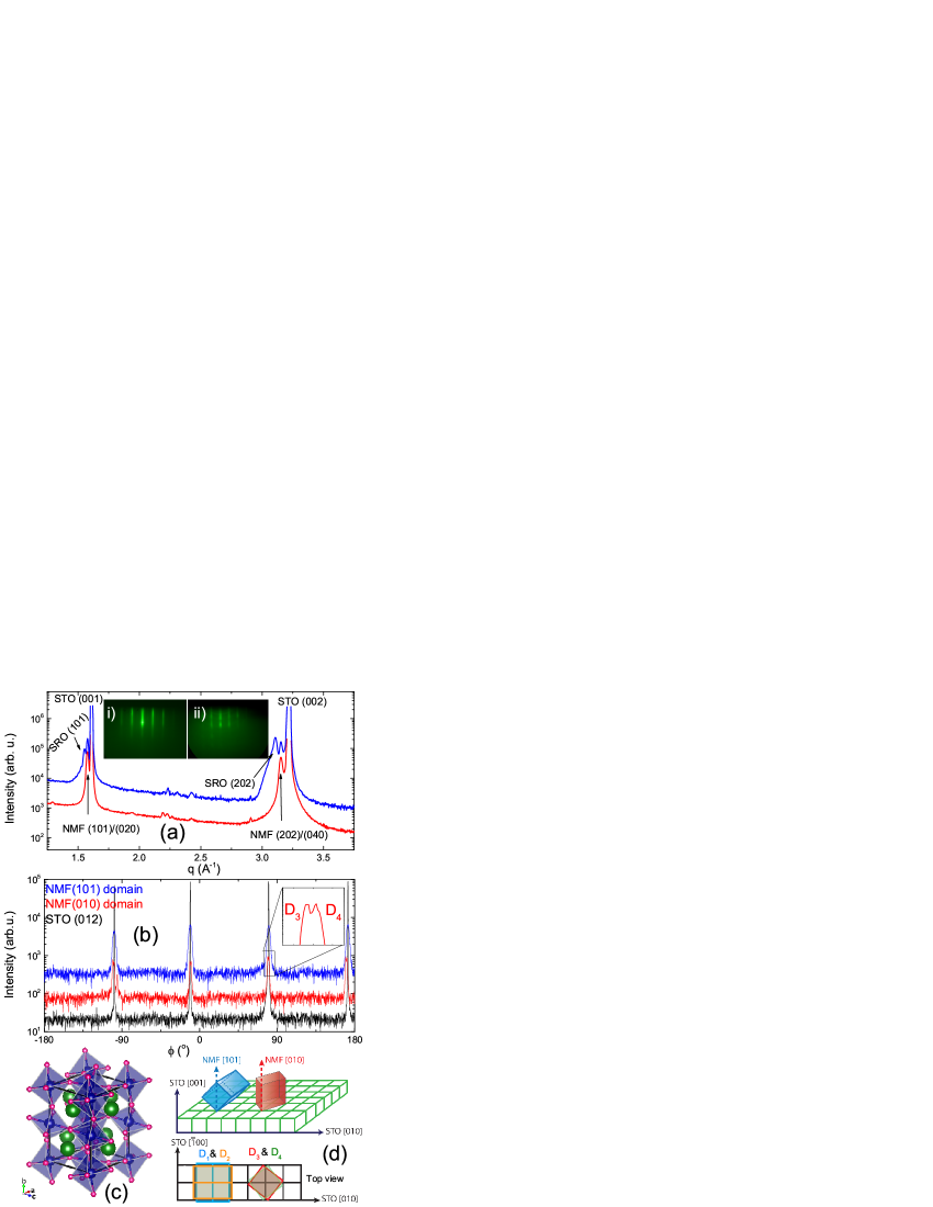
NaMnF3 (NMF) is another fluoride compound that is possibly MF with ME coupling. The NMF crystal structure is described by the orthorhombic space group Pnma. At room temperature, the lattice constants are Å, Å, and Å (Fig. 1a).Ratuszna, Majewska, and Lis (1989) In the pseudo-cubic unit cell, the corresponding lattice parameters are Å and Å. NMF exhibits G-type antiferromagnetism of the Mn magnetic moments centered within tilted MnF6 octahedra, with additional weak ferromagnetic canting.Ratuszna, Majewska, and Lis (1989); Pickart, Alperin, and Nathans (1964); Shane, Lyons, and Kestigian (1967) The Néel temperature has been reported to be K. Teaney, Blackburn, and Stevenson (1962); Shane, Lyons, and Kestigian (1967); Pickart, Alperin, and Nathans (1964); Daniel et al. (1995); Carpenter, Sangregorio, and O’connor (1999); Du et al. (2007) Recent computational work predicted a ferroelectric instability in NMF originating from Na displacements (the A-site perovskite cation in the ABF3 structure). Calculations assuming that a cubic substrate forces the and lattice parameters to be equal to each other have shown that the soft polar mode freezes, resulting in a transformation to the polar space group which causes a polarization of C/cm2 along the long axis . Calculations also indicate that can be enhanced by negative or positive strains (12 Ccm2 at % strain 9 C/cm2 at % strain).Garcia-Castro et al. (2014); Garcia-Castro, Romero, and Bousquet (2016) A weak ferromagnetic phase and an amplification of ME coupling are also expected in the strained films, with a ME response comparable to Cr2O3.Garcia-Castro, Romero, and Bousquet (2016) Therefore, NMF is an attractive ME material because its ferroelectricity can be modulated by strain and is not subject to the rule because there is no displacement of the Mn ion from the center of the MnF6 octahedra.
Here we report on the growth of NMF thin films on cubic SrTiO3 (STO) substrates and on SrRuO3 (SRO) layers, their weak ferromagnetism (FM) below the , and their short range dipolar order. NMF thin films approximately 50 nm thick were grown on pre-polished single crystal (001) STO substrates ( Å) by molecular beam epitaxy (MBE) by co-depositing NaF and MnF2 in an ultra-high vacuum chamber with growth pressure Torr. Atomically flat surface and single termination of STO substrates was achieved by the combination of two thermal annealing steps and a de-ionized (DI) water treatment.Connell et al. (2012) For additional details of the growth process, see supplementary material. The crystallography of the substrate and film surfaces was monitored in-situ using reflection high energy electron diffraction (RHEED). Further crystallographic characterization was carried out ex-situ using x-ray diffraction (XRD) and x-ray reflectivity (XRR) techniques using a rotating anode source with a graphite bent crystal monochromator optimized for Cu Kα radiation. The surface morphology was studied by atomic force microscopy (AFM). Magnetic measurements were performed using a superconducting quantum interference device (SQUID) magnetometer with the substrate signal subtracted by performing identical measurements on a blank substrate.
Dielectric measurements of NMF films were performed by first depositing a 30 nm SRO film on the STO substrate as a bottom electrical contact via pulsed laser deposition (PLD) in a separate vacuum chamber. The SRO was grown at a substrate temperature of 600 ∘C in 100 mTorr O2 partial pressure. A 150 nm NMF thin film was then deposited on the SRO using the conditions described above. The dielectric constant was measured using a lock-in amplifier in the frequency range of 100 Hz to 100 kHz from 10 K to room temperature using a cryostat and an ac voltage amplitude of mV. Similar results were obtained for mV.
The best film quality was achieved at = 250 and 300 ∘C as determined from XRD and RHEED. Figure 1a shows the XRD scan for a film grown at ∘C. The out-of-plane lattice parameters were 3.989 Å and 3.982 Å, and the rocking curve full width at half maximum (FWHM) values were 1.32∘ and 2.23∘ for NMF/STO and NMF/SRO films, respectively (see supplementary material). The positions of the SRO peaks were consistent with data in the literature.Kim, Kang, and Je (2001) XRR data (supplementary material) were fitted using GenX software for the NMF/STO filmBjörck and Andersson (2007) to obtain a NMF thickness of 51.76 nm and a NMF surface surface roughness of 0.4 nm. Streaky RHEED patterns (Fig. 1a inset i) confirmed that the NMF/STO film was smooth and crystalline while the NMF/SRO sample also had streaky patterns with a somewhat fuzzy streaky background (Fig. 1a inset ii).
Using the Pnma NMF structure, reflections associated with -axis pointing out-of-plane [NMF(010)/STO(001)] as well as in-plane [NMF(101)/STO(001)] domains were identified via XRD -scans and reciprocal space maps (RSMs) (the corresponding (010) and (101) lattice parameters are virtually identical; see supplementary material Fig. S4 for RSM data). These results indicate the absence of = distortion in the NMF/STO film for both of these domains. The measured lattice parameters for NMF(010)/STO(001) and NMF(101)/STO(001) domains were Å, Å, and Å and Å, Å, and Å respectively (see Table S1 in the supplementary material). Figure 1b shows the -scans of the reflection of the NMF(101) and NMF(010) domains along with (012) reflections of the substrate. In both NMF domains, four peaks separated by were observed, meaning that two NMF phases with orthogonal axes were present. For NMF(010) domains, the orthorhombic and axes STO [110]. For NMF(101) domains, the axis commensurately aligns STO [010] and [00] (labeled D1 and D2 in Fig. 1d). For the NMF(010) domains, each reflection was additionally comprised of two peaks separated by (Fig. 1b, inset). Therefore, each NMF(010) domain was actually comprised of two in-plane twin domains rotated by about the surface normal with respect to each other (labeled D3 and D4 in Fig. 1b inset and 1d top view). Similar epitaxies of orthorhombically distorted perovskite oxide films on STO have been reported elsewhere.Kim, Kang, and Je (2001); Martí et al. (2008); Daumont et al. (2009); Scola et al. (2011)
For the NMF/SRO sample, epitaxy could not be confirmed by -scans or RSM, despite the streaky RHEED pattern in Fig. 1a. This indicates that the bulk of NMF was highly disordered, with small domains. Because of the similarity between STO and SRO, however, it is reasonable to assume that the strain in the NMF/SRO sample was not too different from the NMF/STO sample.
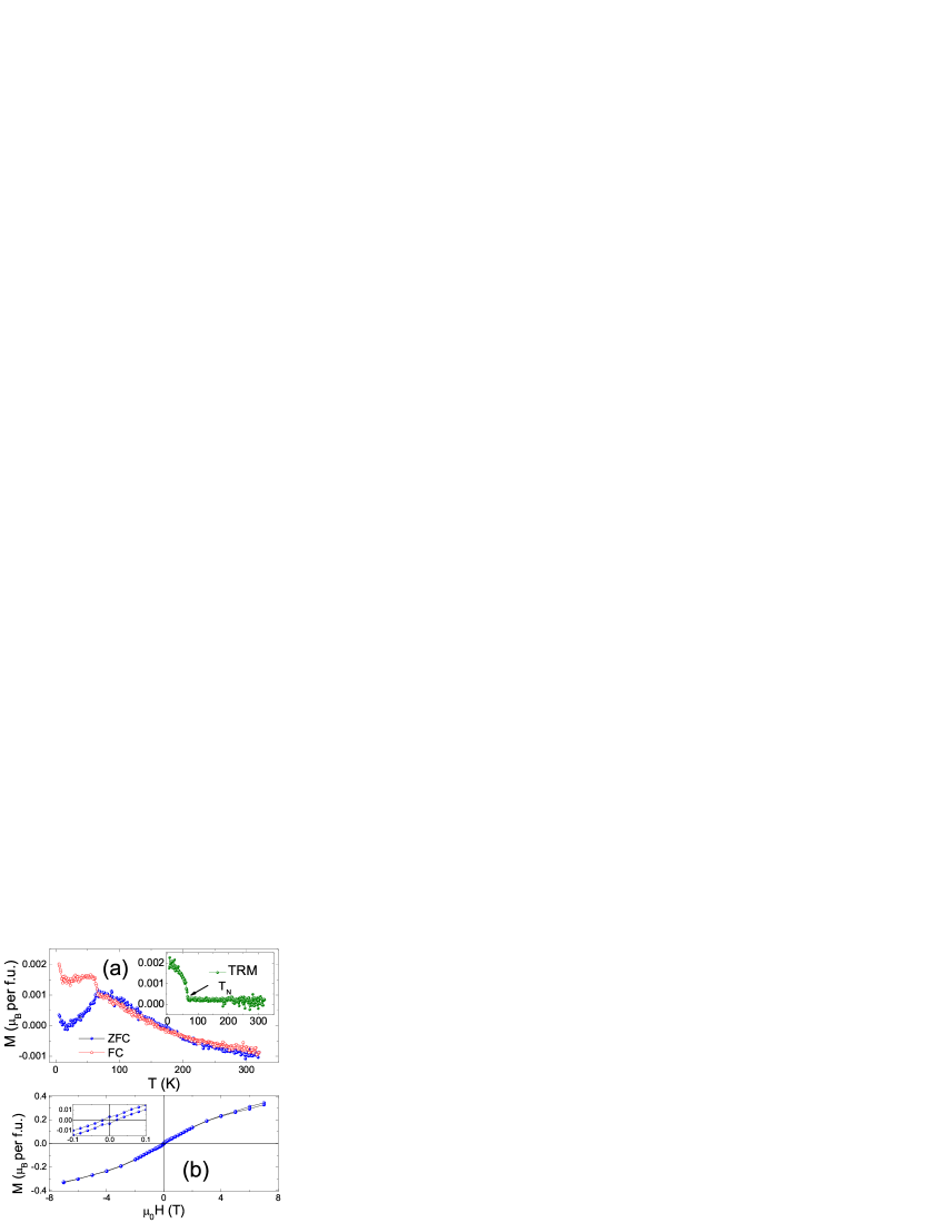
The temperature-dependent magnetization measurements on NMF/STO were carried out by first cooling the samples from room temperature to 5 K in , and then measuring the magnetic moment as a function of in kOe applied in-plane along the STO [001] direction while warming up to 320 K (zero-field cooled, ZFC). Then the measurements were continued while cooling in the same down to 5 K (field cooled, FC). Subsequently, the thermoremanent magnetization (TRM) was measured while warming in . ZFC and FC data in Fig. 2a show a Curie-Weiss-like increase with decreasing temperature until the ZFC data peak at K. On the other hand, the FC decreases sharply below K, in good agreement with theoryGarcia-Castro et al. (2014) and previous experimental work.Teaney, Blackburn, and Stevenson (1962); Shane, Lyons, and Kestigian (1967); Pickart, Alperin, and Nathans (1964); Daniel et al. (1995); Carpenter, Sangregorio, and O’connor (1999) This split between ZFC and FC magnetizations below 66 K is consistent with weak FM below , in agreement with previous studies of NMF nanoparticles and nanoplates.Carpenter, Sangregorio, and O’connor (1999); Du et al. (2007) The TRM data have a Brillouin-like increase below , confirming the weak ferromagnetic nature of the transition. Fig 2b shows the in-plane magnetization hysteresis loop measured at 5 K with the diamagnetic response from the substrate subtracted. The behavior is consistent with weak FM, including an S-shaped loop with a lack of saturation in magnetic fields of up to 7 T and a remanent magnetization in the low field region (Fig. 2b, inset).

Figure 3c and d shows the dielectric permittivity as a function of for the 150 nm thick NMF/SRO film at frequencies from 1 to 78 kHz. The response at 0.1 kHz almost overlaps with that at 1 kHz so it is not shown. At large frequencies, the increase of the real part of the dielectric permittivity at low is superimposed with a broad maximum whose position shifts to lower with decreasing frequency . The imaginary part of dielectric permittivity, , also shows a peak that shifts to lower and becomes narrower with decreasing . This behavior implies a strong relaxation of the dielectric permittivity and resembles properties of relaxor ferroelectrics,Bokov and Ye (2006) but the frequency dependence of the position of the maximum of , , is much stronger than is typically observed in relaxors.Samara (2003) In our case, shifts more than 200 K in only two frequency decades.
To gain more insight in relaxation dynamics, we analyzed dependence of . At low , follows a dependence which is due to a non-zero dc conductivity (Fig. 3b). Also, a typical relaxation maximum is observed for kHz, whose position shifts to lower as decreases. The behavior shows a step-like increase at frequencies where is a maximum. As decreases below 52 K, another relaxation peak seems to appear at a higher frequency. However, this peak was not within our experimental window down to the lowest , and only the low- wing is visible.
Assuming a Debye-like dielectric relaxation, the broad peaks (steps) in the () data indicate the existence of a distribution of relaxation times. Using the Cole-Cole dispersion law,Kremer and Schönhals (2003)
| (1) |
where is an effective characteristic relaxation time, is the dielectric permittivity at very high frequencies, is the relaxation strength, and () indicates the width of the relaxation time distribution ( corresponds to a Debye relaxation with a single relaxation time). The values of , extracted from the position of the maximum of , , are shown in Figs. 3e-f. cannot be satisfactory fitted either by an Arrhenius law,
| (2) |
or by a Vogel-Fulcher law applicable to typical relaxor FE,
| (3) |
where is Boltzmann’s constant and is an activation energy, as seen in Fig. 3e. In the case of Eq. 2, the quality of the fit is low, while the fit to Eq. 3 results in an unphysical negative value of the freezing temperature, . On the other hand, is described well by the power law equation
| (4) |
The best fit (Fig. 3f) yields , s, and a transition temperature K. The value of is close to that describes the divergence of the relaxation time for an order-disorder phase transition in the classical mean-field approximation.Lines and Glass (2004) The actual transition temperature could be much lower than 8 K because only the behavior for was observed. Interestingly, in canonical ferroelectrics the relaxation dynamics corresponding to such transition are typically observed in the GHz frequency range, indicating that relaxing dipolar entities are relatively large and slowly fluctuating microscopic regions spanning several unit cells.
Large dielectric dipolar regions could form because of the diffusion of a FE soft modeGarcia-Castro et al. (2014); Garcia-Castro, Romero, and Bousquet (2016) as a result of the disorder in the NMF/SRO film. Although the NMF/STO film has only a small strain, local measurements like piezoelectric force microscopy (PFM) need to be performed to verify ferroelectricity because of the lack of an electrically conductive bottom layer. In adddtion, further research is required to obtain a tetragonal lattice distortion in NaMnF3 thin films to verify the large ferroelectric polarization predicted by theory.Garcia-Castro et al. (2014); Garcia-Castro, Romero, and Bousquet (2016)
See supplementary material for details of the growth procedure and structural characteristics of the films.
This work was supported by the National Science Foundation (grant # 1434897) and the WVU Shared Research Facilities. We thank A. H. Romero and C. Chen for helpful discussions.
References
- Eerenstein, Mathur, and Scott (2006) W. Eerenstein, N. Mathur, and J. F. Scott, Nature 442, 759 (2006).
- Fiebig (2005) M. Fiebig, Journal of Physics D: Applied Physics 38, R123 (2005).
- Cherepov et al. (2014) S. Cherepov, P. Khalili Amiri, J. G. Alzate, K. Wong, M. Lewis, P. Upadhyaya, J. Nath, M. Bao, A. Bur, T. Wu, G. P. Carman, A. Khitun, and K. L. Wang, Applied Physics Letters 104, 082403 (2014).
- Cheong and Mostovoy (2007) S.-W. Cheong and M. Mostovoy, Nature materials 6, 13 (2007).
- Hayes et al. (2016) P. Hayes, S. Salzer, J. Reermann, E. Yarar, V. Röbisch, A. Piorra, D. Meyners, M. Höft, R. Knöchel, G. Schmidt, and E. Quandt, Applied Physics Letters 108, 182902 (2016).
- Zhao et al. (2006) T. Zhao, A. Scholl, F. Zavaliche, K. Lee, M. Barry, A. Doran, M. Cruz, Y. Chu, C. Ederer, N. Spaldin, et al., Nature materials 5, 823 (2006).
- Park et al. (2007) T.-J. Park, G. C. Papaefthymiou, A. J. Viescas, A. R. Moodenbaugh, and S. S. Wong, Nano Letters 7, 766 (2007).
- Yang et al. (2016) W.-G. Yang, N. A. Morley, J. Sharp, Y. Tian, and W. M. Rainforth, Applied Physics Letters 108, 012901 (2016).
- Hwang et al. (2015) J. S. Hwang, J. Y. Cho, S. Y. Park, Y. J. Yoo, P. S. Yoo, B. W. Lee, and Y. P. Lee, Applied Physics Letters 106, 062902 (2015).
- Scott and Blinc (2011) J. F. Scott and R. Blinc, Journal of Physics: Condensed Matter 23, 113202 (2011).
- Cohen (1992) R. E. Cohen, Nature 358, 136 (1992).
- Ravez (2000) J. Ravez, Comptes Rendus de l’Académie des Sciences - Series {IIC} - Chemistry 3, 267 (2000).
- Borisov et al. (2016) P. Borisov, T. A. Johnson, A. C. García-Castro, A. KC, D. Schrecongost, C. Cen, A. H. Romero, and D. Lederman, ACS Applied Materials & Interfaces 8, 2694 (2016).
- Ratuszna, Majewska, and Lis (1989) A. Ratuszna, K. Majewska, and T. Lis, Acta Crystallographica Section C 45, 548 (1989).
- Pickart, Alperin, and Nathans (1964) S. Pickart, H. Alperin, and R. Nathans, Journal de Physique 25, 565 (1964).
- Shane, Lyons, and Kestigian (1967) J. R. Shane, D. H. Lyons, and M. Kestigian, Journal of Applied Physics 38, 1280 (1967).
- Teaney, Blackburn, and Stevenson (1962) D. Teaney, J. Blackburn, and R. Stevenson, Bull. Am. Phys. Soc. 7, 201 (1962).
- Daniel et al. (1995) P. Daniel, M. Rousseau, A. Desert, A. Ratuszna, and F. Ganot, Phys. Rev. B 51, 12337 (1995).
- Carpenter, Sangregorio, and O’connor (1999) E. E. Carpenter, C. Sangregorio, and C. J. O’connor, Molecular Crystals and Liquid Crystals Science and Technology. Section A. Molecular Crystals and Liquid Crystals 334, 641 (1999).
- Du et al. (2007) Y.-P. Du, Y.-W. Zhang, Z.-G. Yan, L.-D. Sun, S. Gao, and C.-H. Yan, Chemistry – An Asian Journal 2, 965 (2007).
- Garcia-Castro et al. (2014) A. C. Garcia-Castro, N. A. Spaldin, A. H. Romero, and E. Bousquet, Phys. Rev. B 89, 104107 (2014).
- Garcia-Castro, Romero, and Bousquet (2016) A. C. Garcia-Castro, A. H. Romero, and E. Bousquet, Phys. Rev. Lett. 116, 117202 (2016).
- Connell et al. (2012) J. G. Connell, B. J. Isaac, G. B. Ekanayake, D. R. Strachan, and S. S. A. Seo, Applied Physics Letters 101, 251607 (2012).
- Kim, Kang, and Je (2001) S. S. Kim, T. S. Kang, and J. H. Je, Journal of Applied Physics 90, 4407 (2001).
- Björck and Andersson (2007) M. Björck and G. Andersson, Journal of Applied Crystallography 40, 1174 (2007).
- Martí et al. (2008) X. Martí, F. Sánchez, V. Skumryev, V. Laukhin, C. Ferrater, M. García-Cuenca, M. Varela, and J. Fontcuberta, Thin Solid Films 516, 4899 (2008).
- Daumont et al. (2009) C. J. M. Daumont, D. Mannix, S. Venkatesan, G. Catalan, D. Rubi, B. J. Kooi, J. T. M. D. Hosson, and B. Noheda, Journal of Physics: Condensed Matter 21, 182001 (2009).
- Scola et al. (2011) J. Scola, P. Boullay, W. Noun, E. Popova, Y. Dumont, A. Fouchet, and N. Keller, Journal of Applied Physics 110, 043928 (2011).
- Bokov and Ye (2006) A. Bokov and Z.-G. Ye, in Frontiers of Ferroelectricity (Springer, 2006) pp. 31–52.
- Samara (2003) G. A. Samara, Journal of Physics: Condensed Matter 15, R367 (2003).
- Kremer and Schönhals (2003) F. Kremer and A. Schönhals, eds., Broadband Dielectric Spectroscopy (Springer, Berlin, Heidelberg, 2003).
- Lines and Glass (2004) M. E. Lines and A. M. Glass, Principles and applications of ferroelectrics and related materials (Claredon Press, Oxford, 2004).