A Computational Framework for Automation of Point Defect Calculations
Abstract
A complete and rigorously validated open-source Python framework to automate point defect calculations using density functional theory has been developed. The framework provides an effective and efficient method for defect structure generation, and creation of simple yet customizable workflows to analyze defect calculations. The package provides the capability to compute widely-accepted correction schemes to overcome finite-size effects, including (1) potential alignment, (2) image-charge correction, and (3) band filling correction to shallow defects. Using Si, ZnO and In2O3 as test examples, we demonstrate the package capabilities and validate the methodology.
I Introduction
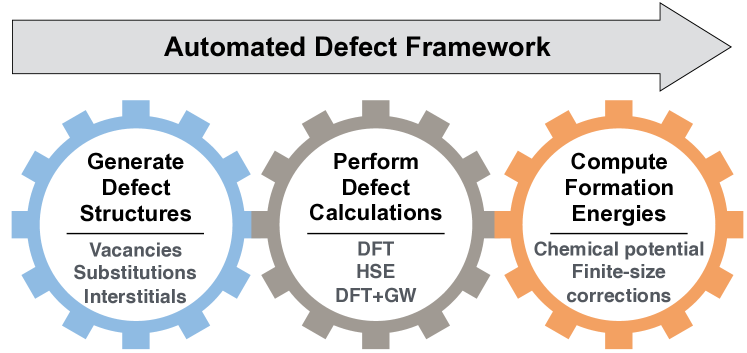
In semiconductor materials, point defects play a vital role in determining their properties and performance, particularly in microelectronics,del Alamo (2011) optoelectronics,Yu et al. (2016) and thermoelectricsYan et al. (2015) related applications. The dominant point defects and their concentrations are determined from the defect formation energies, which can be predicted with reasonable accuracyLejaeghere et al. (2016) using first-principles methods such as density functional theory (DFT). Therefore, computational modeling of point defects is increasingly becoming an indispensable tool to understand and predict behavior of semiconductors.Van de Walle (2004); Alkauskas et al. (2011); Freysoldt et al. (2014) Modern approaches to point defect calculations uses DFT and are typically based on the supercell approach.Alkauskas et al. (2011); Freysoldt et al. (2014) With the goal of accelerating the design and discovery of materials by large-scale deployment of defect calculations, we have developed a computational framework (Fig. 1) to automate supercell-based point defect calculations with DFT. Our approach successfully addresses two main challenges of automating point defect calculations: (1) generation of defects structures including vacancies, substitutional defects and interstitials, and (2) application of the finite-size and band gap corrections.
In the context of structure generation, creating supercells with vacancies and substitutional defects is relatively straightforward. In contrast, identifying likely locations of interstitials is much more challenging because of the large number of interstitialcy sites, especially in complex, multinary systems. In addition, interstitials might adopt complex configurations, including the split or dumbbell where the interstitial is associated with a off-site lattice atom. To address these challenges, we have developed an efficient scheme based on Voronoi tessellation;Rycroft (2009) the scheme considers corners, edge and face centers of the Voronoi polyhedra as likely sites for interstitials. We demonstrate that, upon relaxing the structure, this scheme successfully discovers both the symmetric and general Wyckoff positions as well as the split interstitial configurations. Our implementation of this scheme is independent of pymatgenOng et al. (2013) where Voronoi tessellation is also employed. Here we will discuss the algorithm in detail and validate the Voronoi-driven approach to identify interstitial sites.
Within the supercell approach to calculate the defect formation energies, finite-size artifacts need to be removed using carefully designed correction schemes. We have implemented tools to calculate the following finite-size corrections: (1) potential alignment, (2) image-charge correction, and (3) band filling correction to address Moss-Burstein-type effects. We follow the widely used and tested approach of Lany and ZungerLany and Zunger (2008, 2009) out of the several others that addresses the same issues.Makov and Payne (1995); Freysoldt et al. (2011); Taylor and Bruneval (2011); Komsa et al. (2012); Kumagai and Oba (2014) However, the automated framework is highly modular so that other correction schemes can be easily implemented including computation of defect formation energies using series of supercell sizes in order to extrapolate the values to the infinitely large supercell. In addition, the framework employs fitted elemental-phase reference energies (FERE) Lany (2008); Stevanović et al. (2012) to compute elemental chemical potentials.
Beyond the finite-size effects, another source of inaccuracy arises from the well-known DFT band gap problem. Accurate band gaps are needed to correctly describe the formation energy of charged defects as a function of the electronic chemical potential i.e., Fermi energy. We employ state-of-the-art GW quasiparticle energy calculationsHedin (1965) to compute band edge shifts (relative to the DFT-computed band edges). The band edge shifts are used to correct the defect formation energy in multiple charge states. The automated framework is also capable of performing defect calculations with DFT hybrid functionals.Perdew et al. (1996a); Heyd et al. (2003) However, supercell defects calculations with hybrid functionals have sources of uncertainty arising from the choice of input parameters (e.g. fraction of exchange) and have considerable computational overheads.Peng et al. (2013) Therefore, we have implemented a DFT+GW approach for calculating defect formation energy that has been shown to be as accurate as calculations with hybrid functionals.Peng et al. (2013) Finally, we illustrate and validate the automated computational framework by considering the set of three well-studied semiconductor materials, Si, ZnO, and In2O3 with a total of 17 unique interstitial and vacancy structures in multiple charged states. We show that our results on defect formation energies and charge defect transition levels in Si, ZnO and In2O3 agree well with the literature. The framework successfully identifies the known intrinsic interstitial and vacancy structures in Si, ZnO and In2O3. In addition, it discovers interstitial structures in In2O3, with formation energies 0.5 eV above that of previously known interstitial structures.
II Overview of the Automated Defect Framework
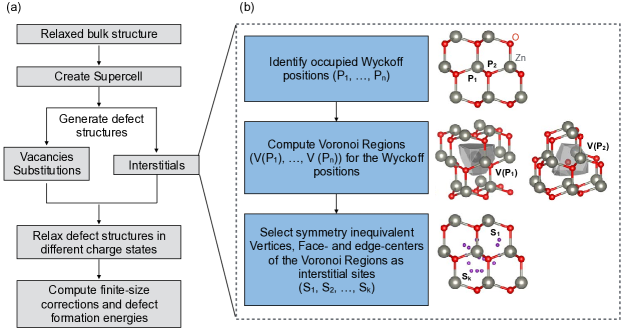
Figure 2(a) presents a workflow of the automated framework, including generation of defect structures, relaxation of defect supercells within DFT using the PyLada framework,d’Avezac et al. (2010) and determination of finite-size and band gap corrections to compute the defect formation energies. In this section, we describe each component of the framework and provided technical details.
II.1 Generate Defect Structures
The workflow takes the fully-relaxed primitive cell as an input to create supercells. To create a vacancy or substitutional defect in supercell, the occupied Wyckoff positions (lattice-sites) for all atom types in the supercell are identified. Then the corresponding atom is removed or substituted with an impurity atom, to generate vacancy or substitutional defect. Finally, the first nearest-neighbor atoms to the vacancy or substitutional site are randomly displaced ( 0.1 Å) to break the underlying site symmetry and thereby, ensuring the non-symmetric configurations of the defects are properly captured. The Voronoi tesselation,Rycroft (2009); Smith (2015) scheme is employed to identify likely interstitial sites. Voronoi region is the volume that encloses the points closest to a given lattice site than to any other lattice site for . Mathematically, it is defined asRycroft (2009)
| (1) |
where, is the Voronoi region associated with , and specifies the minimum distance between a general point and . To create an interstitial, Voronoi regions (Eq. 1) are computed across each occupied Wyckoff positions, and symmetry inequivalent vertices, face, and edge centers of the Voronoi regions are chosen as the candidate sites for the interstitials. The number of candidate interstitial sites depends on the symmetry of the crystal structure. The lower the symmetry and the more complex the crystal structure, the larger the number of sites. For example, in In2O3 (space group Ia-3, 40 atoms in primitive cell), we find that some of the faces of the Voronoi region are very small, resulting in sampled interstitial sites very close to each other. Therefore a minimum tolerance of 0.5 Å is used while determining symmetry inequivalent sites. The procedure is described in Fig. 2(b), with ZnO as an example structure.
II.2 Perform Defect Calculations
DFT calculations are performed with the projector augmented wave (PAW) methodBlöchl (1994) as implement in VASP.Kresse and Furthmüller (1996) The Perdew Burke Ernzerhof (PBE) exchange correlation functionalPerdew et al. (1996b) is used both in GGA (Si, In2O3) and GGA+U spin polarized calculations (ZnO, U(Zn-d) = 6 eV). The plane wave energy cutoff of 340 eV, and a Monkhorst-Pack k-point samplingMonkhorst and Pack (1976) is used. The structures are taken from the inorganic crystal structure database (ICSD)Belsky et al. (2002) and fully relaxed using the procedure outlines in Ref.18. Defect calculations are performed on 216, 96 and 80 atoms supercell for Si, ZnO, and In2O3, respectively. A -centered 2x2x2 k-point mesh is used for all supercell calculations, except for Si, for which only single point only calculations are performed. The low-frequency total (electronic + ionic) dielectric constant is obtained following the procedure in Ref.22. For hybrid functional (HSE06Krukau et al. (2006)) calculations in Si, the exchange-mixing, is used. GW calculations are performed on the DFT relaxed structures, with the unit cell vectors re-scaled to match the experimental lattice volume.Peng et al. (2013) The high-throughput DFT calculations are performed using PyLada,d’Avezac et al. (2010) a powerful Python framework for the constructing workflows, and managing large number of calculations. PyLada also offers variety of useful tools for constructing crystal structures, for manipulating functionals and extracting their output, and analyzing results.Gorai et al. (2016); Stevanović (2016); Deml et al. (2016)
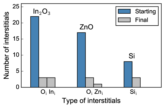
As summarized in Fig. 2(a), the workflow starts with fully relaxing (volume, cell shape and ionic positions) the bulk primitive cell. Dielectric constant, and GW calculations are performed on the relaxed primitive cell. Point defects are then created in the bulk supercell followed by relaxation (only ionic positions) of defect structures in multiple charge states. Calculations of interstitial defects are performed in two steps: (1) All candidate interstitials (shown as starting interstitials in Fig. 3) are relaxed in the neutral charge state, (2) followed by relaxation of only unique interstitials (shown as final interstitials in Fig. 3) in multiple charge states. Unique interstitial structures are determined based on: (1) the total energy, (2) space group, and (3) the number of neighboring atoms. Finally, the defect formation energies are computed as discussed in the next section.
II.3 Compute Defect Formation Energy
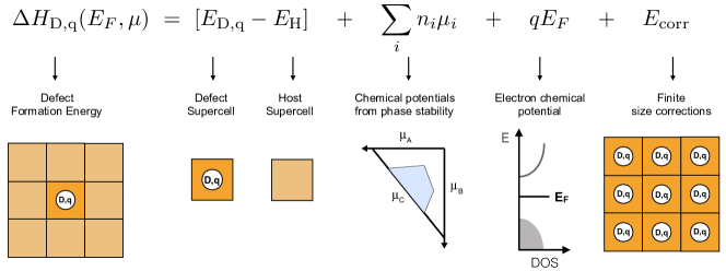
The formation energy of the defect D in the charge state q is calculated as
| (2) |
where, and are the total DFT energies of the defect and host supercell, respectively. is the chemical potential of the atom (host or impurity) of type added () or removed () from the host supercell to form the defect. is the Fermi energy, and is the term that account for the finite-size corrections, within the supercell approach. A schematic of Eq. 2, representing computation of the defect formation energy from supercell to the dilute limit is shown in Fig. 4.
II.3.1 Chemical Potential and Phase Stability
Chemical potentials reflect the energy of the reservoirs for the atoms that are involved in creating the defect. Numerical values of the chemical potentials () depend on their implicit references, , which here are obtained from the reference FERE Lany (2008); Stevanović et al. (2012) energies, . FERE energies are also used to compute the formation enthalpy () of all the competing phases which are needed to determine the thermodynamic limits of the chemical potential . The computed and values are summarized in table 1. For Si, (Si) = -5.41 eV/atom is used and to determine the limits to the respective elemental chemical potentials, we apply the following thermodynamic stability conditions, (ZnO) and (In2O3), in ZnO and In2O3, respectively.
II.3.2 Electron Chemical Potential
Fermi energy is the measure of the chemical potential of electrons. It is defined with respect to the host valence band maximum (VBM), , and is bounded by the conduction band maximum (CBM). DFT (GGA) band gaps are corrected by determining the band edge shifts, for the VBM, and for the CBM, from the GW quasiparticle energy calculations.Peng et al. (2013) The computed band gaps are also summarized in table 1.
| System | Lattice constant | Dielectric constant | Chemical potential | Hf | Band Gap (eV) | |
| (Å) | (eV) | (eV) | GW (GGA) | |||
| Si | 5.46 | 13.36 | -5.41 | 1.29 (0.62) | ||
| Expt. 111References34; 35 | 5.43 | 11.7 | 1.17 | |||
| ZnO | = 3.28, | 5.53 | 5.12 | O = -4.76, | -3.63 | 3.25 (0.73) |
| = 5.30 | Zn = -0.56 | |||||
| Expt. 222References36; 37; 38; 39 | = 3.25, = 5.2 | 3.7 - 3.8 | 4 - 5.13 | -3.62 | 3.44 | |
| In2O3 | 10.28 | 4.90 | 6.47 | O = -4.76 | -9.45 | 2.47 (0.96) |
| In = -2.31 | ||||||
| Expt. 333References40; 41; 42; 38; 43; 44; 45; 46 | 10.1 | 4.08 | 4.8 | -9.6 | 2.67 - 3.1 | |
II.3.3 Finite-size Corrections
Finite size corrections are implemented in the package following the approach of Lany and Zunger.Lany and Zunger (2008, 2009) Correction schemes focusing on single physical effect are considered.Freysoldt et al. (2014) These include:
Potential alignment correction, which restores the relative position of the host VBM in the calculations of charged defect (affecting the Fermi energy). Correction to the defect formation energy due to the potential alignment is given asLany and Zunger (2008)
| (3) |
where the reference potentials, , for the charged defect (D,q) and the pure host (H) are determined from the (local) atomic-sphere-averaged electrostatic potentials at the atomic sites farther away from the defect.Lany and Zunger (2008)
Image-charge correction, is needed to correct for the spurious electrostatic interactions of the charged defect (in the presence of homogeneous compensating background charge) with its periodic images. This is given asLany and Zunger (2009)
| (4) |
where is the linear supercell dimension (volume, ), is the static dielectric constant (electronic + ionic), and , are the Madelung constant, and shape factor, respectively, for the adopted supercell geometry.
Band filling correction, correct for the Moss-Burstein-type band filling effects that appear due to high defect concentrations in a typical finite-size supercell calculations.Lany and Zunger (2008) For a given k-point set (weighted sum, ) and band occupations, , the correction for the shallow donor is computed asLany and Zunger (2008)
| (5) |
and for shallow acceptor
| (6) |
where, are the band energies in the defect calculation, is the CBM and is the VBM energy of the pure host after potential alignment correction.
III Examples
III.1 Silicon
Silicon has been the focus of both experimentalWatkins (1997); Bracht et al. (2007) and theoreticalBaraff et al. (1979); Car et al. (1984); Bar-Yam and Joannopoulos (1984); Puska et al. (1998); Wright (2006); Rinke et al. (2009); Śpiewak and Kurzydłowski (2013) research on intrinsic point defects over the past decade. Structure of both silicon vacanciesBaraff et al. (1979); Puska et al. (1998); Wright (2006); Śpiewak and Kurzydłowski (2013) and self-interstitialsCar et al. (1984); Bar-Yam and Joannopoulos (1984); Rinke et al. (2009) has been topic of interest as they exists in several stable and metastable configurations.
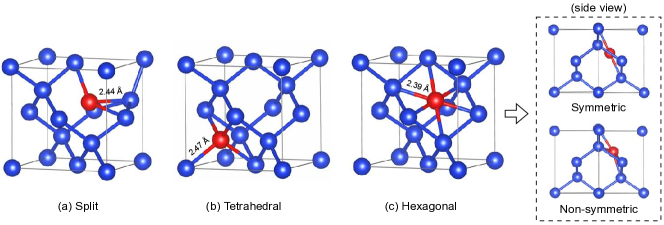
In agreement with the existing literature, we find three distinct silicon self-interstitial structures namely, spit, hexagonal and tetrahedral as shown in Fig. 5, among the starting 7 candidate sites from the defect generation code. Neutral split interstitial has the lowest formation energy (3.25 eV), followed by hexagonal interstitial with energy 0.2 eV higher. Hexagonal interstitial lies along the [111] direction and sit symmetrically at the center of the hexagon formed by six neighboring Si lattice atoms. Hexagonal interstitial also exists in a non-symmetric configuration, as shown in the side view in Fig. 5. This configuration is 5 meV lower in energy than the symmetric one, but is unstable and relaxes to tetrahedral geometry in the charge states 1+ and 2+. Metastable hexagonal configuration have been reported in previous DFT calculations,Rinke et al. (2009) referred as ‘displaced hexagonal’ or by C3v site symmetry. Tetrahedral interstitial in the neutral charge state has the highest formation energy, about 0.33 eV higher than the split interstitial. All the distances between the interstitial and the four neighboring Si lattice sites are same and are equal to 2.47 Å.
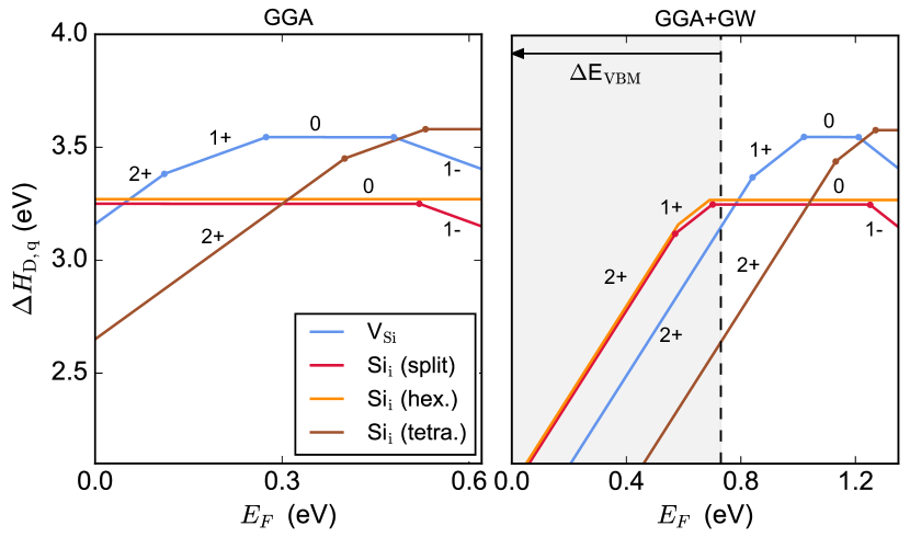
Vacancy structures are analyzed in terms of distances between the neighboring 4 silicon atoms to the vacancy site. It has been reportedWatkins (1997) that silicon vacancy undergo structure reconstruction in different charge states, and form a Negative-U system.Baraff et al. (1979); Watkins (1997) The negative-U behavior implies an energy lowering structural distortion by the presence of a second electron, such that the energy gain more than compensates the e-e repulsive energy cost.Baraff et al. (1979) For the spin-polarized calculations, vacancy in the neutral and 2- charge state relaxes to higher energy configurations, with C2v and D2d point group symmetry, respectively. The inability of spin-polarized calculations to reproduce lower energy point group symmetry of charged vacancies has also been reported in previous LDACorsetti and Mostofi (2011) and GGAŚpiewak and Kurzydłowski (2013) calculations. We observe (2+/1+) and (1+/0) charge transitions for silicon vacancy, instead of the direct (2+/0) charge transition because the computed neutral Si vacancy is in the higher energy configuration compared to its lower energy D2d configuration. However, using spin-polarized HSE calculations on DFT structures, we observe direct (2+/0) charge transition.
Among interstitials, tetrahedral structure is most stable in 2+ charge state, which then transition (-0.27 eV below CBM) to the split structure, which is the most stable configuration for 0 and 1- charge states. The computed defect formation energies and charge transition levels (Fig. 6) for silicon vacancies and interstitials are in good agreement with the reported GGARinke et al. (2009); Corsetti and Mostofi (2011); Śpiewak and Kurzydłowski (2013) and HSE calculations.Weber et al. (2013); Śpiewak and Kurzydłowski (2013) However, their are noticeable difference in the charge defect transition levels between GGA and GGA+GW, mainly due to the band edge positions predicted by the self-consistent GW calculation.Chen and Pasquarello (2014) Similar differences in charge transition levels between LDA and LDA+G0W0 in calculations on silicon interstitials has been reported by Rinke et al.Rinke et al. (2009)
III.2 Zinc Oxide
ZnO is a direct band gap semiconductor and occurs in the ground state wurtzite crystal structure (space group P63mc, 186), with two lattice parameters, and , in the ratio of . The calculated lattice constants and band gap for the wurtzite ZnO are in good agreement with the known experimental measurements, as summarized in table 1. Comprehensive studies of intrinsic vacancy and interstitial structuresJanotti and Van De Walle (2007); Huang et al. (2009) in ZnO has been done in the past. In the following discussion we analyze the defect structures predicted using the automated defect framework and compare our results with the existing literature.
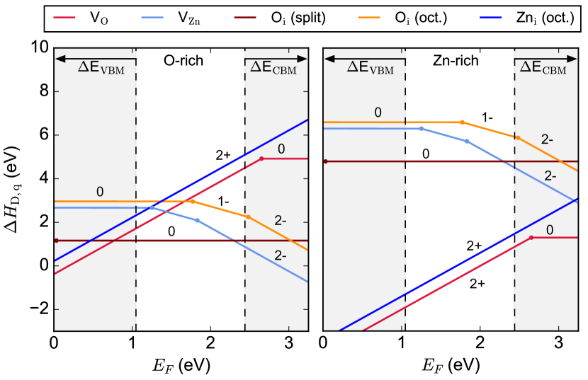
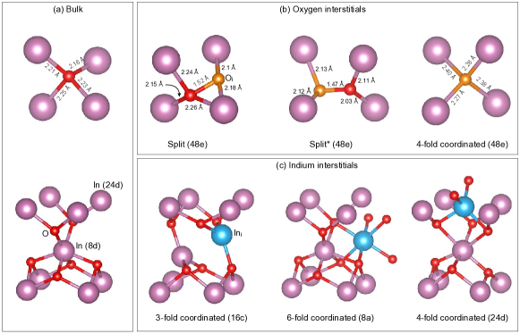
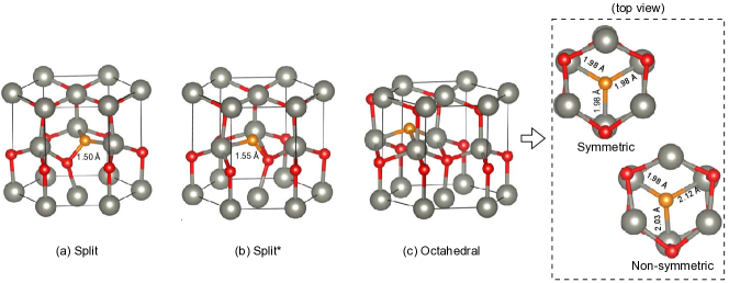
Figure 7 shows the obtained three distinct oxygen interstitial structures out of the starting 17 possibilities for the interstitial sites. Among oxygen interstitials, split interstitial (Fig. 7(a)) has the lowest formation energy. Split interstitial has a metastable configuration (Fig. 7(b), referred here, and in literature as split*Erhart and Albe (2006); Janotti and Van De Walle (2007)) which is 0.21 eV higher in energy than the stable split configuration and relaxes to stable configuration on further relaxation. Octahedral oxygen interstitial lies in the empty channel along [001] Z-axis inside the six member ring formed by O-Zn atoms, Fig. 7(c), and is about 1.8 eV higher in energy than the neutral split interstitial. We find two configurations of octahedral oxygen interstitial as shown in the projection along [001] Z-axis (dashed box) in Fig. 7. The symmetric configuration is 0.3 eV higher in energy than the non-symmetric configuration. The symmetric octahedral is only stable in the neutral charge state and relaxes to non-symmetric configuration for positive and negative charge states. The low energy non-symmetric octahedral configuration has been reported in a previous DFT study,Huang et al. (2009) investigating migration path of oxygen interstitials along [001] direction. With our method we directly find the non-symmetric configuration as the lowest energy octahedral structure.
Zinc interstitial is stable in the octahedral configuration with interstitial atom symmetrically placed at the center of the empty channel along [001] Z-axis, similar to the symmetric octahedral oxygen interstitial. In the relaxed geometry the Zni-O distance is 2.05 Å, and Zni-Zn distance is 2.45Å. Among interstitials split oxygen interstitial is stable in neutral charge state for the whole range of Fermi Energy (Fig. 8). Oxygen interstitials at the octahedral site act as deep acceptors, and have relatively high formation energies compared to Zinc vacancies. Zinc interstitials act as shallow donors, with 2+ charge as the most stable charge state (Fig. 8). But with formation energies as high as 2.6 eV at CBM, even under Zn rich conditions are unlikely to form in substantial concentration.
Both oxygen and zinc in ZnO occupy the 2b Wyckoff position, with 4-fold coordinated tetrahedral geometry. Oxygen vacancy in 2+ charge state shows relatively large outward relaxation of the neighboring Zn atoms, as reported in previous DFT calculations.Janotti and Van De Walle (2007) Oxygen vacancy shows transition from 2+ to 0 charge state, at Fermi energy -0.45 eV below the CBM (Fig. 8), confirming the reported Negative-U character.Janotti and Van De Walle (2007); Lany and Zunger (2007); Oba et al. (2008) Oxygen vacancy act a deep donor, with fully occupied neutral defect state inside the band gap. Zinc vacancy has partially occupied defect states in the band gap, and act as deep acceptor with (0/1-) and (1-/2-) transition level occur at 1.16, and 1.58 eV, respectively above the VBM.
Overall, our approach confirms the known interstitial and vacancy structures in ZnO, and provide a clear picture of the defect energetics and electronic structure consistent with the previous defect calculations. Our next step forward is to investigate the automated point defect framework against In2O3, a relatively complex crystal structure containing 40 atoms in the primitive unit cell.
III.3 Indium Oxide
In2O3 is a direct band gap semiconductor which is widely used as a transparent conducting oxide. Intrinsic defects in In2O3 have received relatively moderate attention both experimentallyDe Wit (1977); De Wit et al. (1977) and theoreticallyLany and Zunger (2007); Ágoston et al. (2009); Liu et al. (2014) compared to silicon and ZnO. It crystalizes in ground state cubic bixbyite structure (space group Ia-3, 206) with indium (Wyckoff positions 8b and 24d) and oxygen (48e) lattice sites in the bulk structure as shown in Fig. 9(a).
Figure 9 displays the oxygen and indium interstitials structures realized using the automated defect framework. We observe three distinct structures for oxygen interstitials (among the initial set of 22 possible candidates), all occupying the general 48e (x, y, z) Wyckoff position in the relaxed structure. Split oxygen interstitial (Fig. 9(b)) is the lowest energy configuration. We find a new split interstitial configuration (referred as split* in Fig. 9(b)) which is stable in the neutral charge state and is about 0.67 eV higher than the lowest energy split interstitial. However split* configuration is unstable in positive charge states and relaxes to the split geometry. Oxygen interstitial bonded to 4 neighboring indium atoms (referred as 4-fold coordinated in Fig. 9(b)) is the highest energy configuration, with energy of about 1.0 eV higher than the split configuration. To our knowledge only the split and 4-fold coordinated oxygen interstitial configuration has been reported in literature.Lany and Zunger (2007) This could be due to the fact that, first, such an exhaustive method to theoretically search interstitials has not been adopted for In2O3, and second, often only the un-occupied Wyckoff positions (16c and 8a) are considered to investigate interstitials in In2O3.Lany and Zunger (2007)
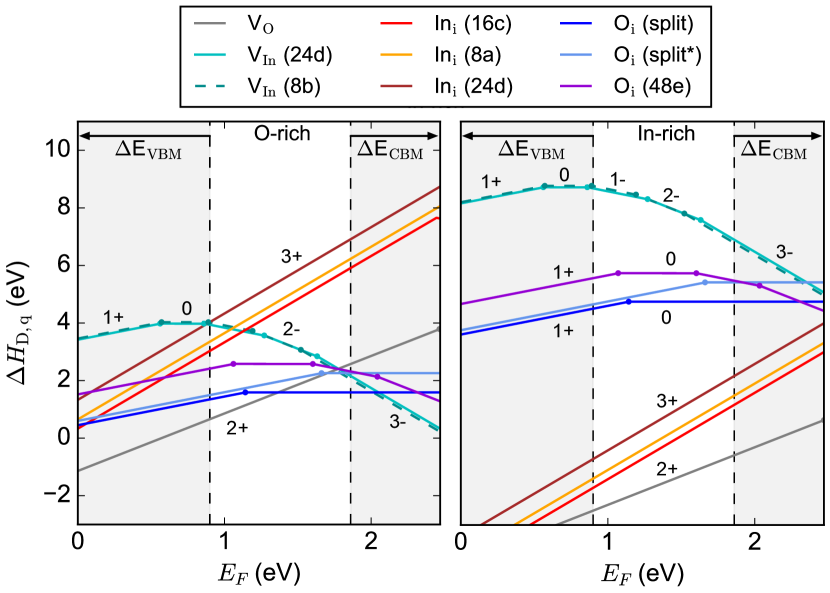
For indium interstitials we also find three distinct configurations (Fig. 9(c)). Lowest energy configuration correspond to indium atom occupying the 16c (0.17, 0.17, 0.17) Wyckoff position, which is 3-fold coordinated to neighboring oxygen atoms (bond length 2.15 Å). Interstitial atom displaces the indium atom originally at the lattice site 8b (with 6-fold coordination) to a similar 16c (0.83, 0.17, 0.34) Wyckoff position with 3-fold coordination. Indium interstitial at 8a (0.5, 0.0, 0.5) Wyckoff position is symmetrically placed in the empty channel between host indium and oxygen atoms along [110] type direction. It is bonded to 6 neighboring oxygen atoms at bond length of 2.24 Å. In neutral charge state its energy is about 0.3 eV higher than 16c configuration. Third indium interstitial configuration occupy the 24d (0.75, 0.25, 0.50) Wyckoff position, and is also placed in the empty channel along [110] type direction. It is bonded to 4 neighboring oxygen atom, two of which are at bond length 2.05 Å, and the other two at 2.18 Å. 24d configuration is highest in energy, with energy 0.83 eV than the 16c configuration in the neutral charge state. To our knowledge, 24d configuration for indium interstitial has never been considered previously, and though it is high in energy, we believe its existence is relevant and crucial because of the entropy at growth temperatures.
In the context of electronic structure, oxygen interstitials has defect states deep inside the band gap, and so as for the indium vacancies (Fig. 10). Indium vacancies have two distinct configurations 8b (0.75, 0.25, 0.25) and 24d (0.75, 0.5, 0.0) both 6-fold coordinated to the neighboring oxygen atoms. Indium interstitials in all structural configurations act as shallow donors, with defect states formed as resonance states above the CBM. Indium interstitial occur in 3+ charge state for the Fermi energy in majority of the band gap, with charge transition levels occur almost at the CBM (Fig. 10). We observe shallow donor type defect states for oxygen vacancy in DFT with 2+ charge state being the most stable within the explored range of the Fermi energy. As discussed previously,Lany and Zunger (2011) defect states in DFT can hybridize strongly with the band edges, and requires self-consistent band gap corrected method such as hybrid functional and defect GW to accurately determine oxygen vacancy charge transition levels. Overall, our results are consistent with previous DFT calculationsLany and Zunger (2007); Liu et al. (2014) in In2O3 and demonstrate the potential of the employed automated point defect framework to discover interstitials structures in complex crystal structures.
IV Summary and future outlook
We have developed an efficient and extensively validated framework to automate point defect calculations. We applied the framework to Si, ZnO and In2O3, and recovered the known intrinsic defect structures as well as their electronic structure properties. Our results demonstrate that the automated defect framework can not only be employed to discover interstitials in complex crystal structures such as In2O3, but also predict accurate defect formation energy of point defects using the implemented finite-size correction schemes. The package is being continuously developed and is hosted on GitHub at https://github.com/pylada/pylada-defects. We believe an automated point defect analysis framework like this will accelerate structure-property prediction by bringing detailed defect understanding to the forefront, and will contribute to more strategic efforts towards tuning the device performance.
Acknowledgements.
We thank Rachel Kurchin for helpful discussions. A. Goyal and V. Stevanovic are funded by the National Science Foundation (NSF) partially under grants DMR-1309980 and CBET-1605495. P. Gorai is funded by the NSF DMR program, grant no. 1334713. H. Peng and S. Lany acknowledges support as part of the Center for the Next Generation of Materials by Design, an Energy Frontier Research Center (EFRC) funded by U.S. Department of Energy (DOE), Office of Science, Basic Energy Sciences. This research used computational resources sponsored by the DOE Office of Energy Efficiency and Renewable Energy and located at the National Renewable Energy Laboratory (NREL).References
- del Alamo (2011) J. A. del Alamo, Nature 479, 317 (2011).
- Yu et al. (2016) X. Yu, T. J. Marks, and A. Facchetti, Nature Materials 15, 383 (2016).
- Yan et al. (2015) J. Yan, P. Gorai, B. Ortiz, S. Miller, S. A. Barnett, T. Mason, V. Stevanović, and E. S. Toberer, Energy Environ. Sci. 8, 983 (2015).
- Lejaeghere et al. (2016) K. Lejaeghere, G. Bihlmayer, T. Bjorkman, P. Blaha, S. Blugel, V. Blum, D. Caliste, I. E. Castelli, S. J. Clark, A. Dal Corso, S. de Gironcoli, T. Deutsch, J. K. Dewhurst, I. Di Marco, C. Draxl, M. Du ak, O. Eriksson, J. A. Flores-Livas, K. F. Garrity, L. Genovese, P. Giannozzi, M. Giantomassi, S. Goedecker, X. Gonze, O. Granas, E. K. U. Gross, A. Gulans, F. Gygi, D. R. Hamann, P. J. Hasnip, N. A. W. Holzwarth, D. Iu an, D. B. Jochym, F. Jollet, D. Jones, G. Kresse, K. Koepernik, E. Kucukbenli, Y. O. Kvashnin, I. L. M. Locht, S. Lubeck, M. Marsman, N. Marzari, U. Nitzsche, L. Nordstrom, T. Ozaki, L. Paulatto, C. J. Pickard, W. Poelmans, M. I. J. Probert, K. Refson, M. Richter, G.-M. Rignanese, S. Saha, M. Scheffler, M. Schlipf, K. Schwarz, S. Sharma, F. Tavazza, P. Thunstrom, A. Tkatchenko, M. Torrent, D. Vanderbilt, M. J. van Setten, V. Van Speybroeck, J. M. Wills, J. R. Yates, G.-X. Zhang, and S. Cottenier, Science 351, aad3000 (2016).
- Van de Walle (2004) C. G. Van de Walle, Journal of Applied Physics 95, 3851 (2004).
- Alkauskas et al. (2011) A. Alkauskas, P. Deák, J. Neugebauer, A. Pasquarello, and C. G. Van de Walle, eds., Advanced Calculations for Defects in Materials (Wiley-VCH Verlag GmbH & Co. KGaA, Weinheim, Germany, 2011).
- Freysoldt et al. (2014) C. Freysoldt, B. Grabowski, T. Hickel, J. Neugebauer, G. Kresse, A. Janotti, and C. G. Van de Walle, Reviews of Modern Physics 86, 253 (2014).
- Rycroft (2009) C. H. Rycroft, Chaos 19 (2009), 10.1063/1.3215722.
- Ong et al. (2013) S. P. Ong, W. D. Richards, A. Jain, G. Hautier, M. Kocher, S. Cholia, D. Gunter, V. L. Chevrier, K. A. Persson, and G. Ceder, Computational Materials Science 68, 314 (2013).
- Lany and Zunger (2008) S. Lany and A. Zunger, Physical Review B 78, 235104 (2008).
- Lany and Zunger (2009) S. Lany and A. Zunger, Modelling and Simulation in Materials Science and Engineering 17, 084002 (2009).
- Makov and Payne (1995) G. Makov and M. Payne, Physical Review B 51, 4014 (1995).
- Freysoldt et al. (2011) C. Freysoldt, J. Neugebauer, and C. G. Van de Walle, Physica Status Solidi (B) 248, 1067 (2011).
- Taylor and Bruneval (2011) S. E. Taylor and F. Bruneval, Physical Review B 84, 075155 (2011).
- Komsa et al. (2012) H.-P. Komsa, T. T. Rantala, and A. Pasquarello, Physical Review B 86, 045112 (2012).
- Kumagai and Oba (2014) Y. Kumagai and F. Oba, Physical Review B - Condensed Matter and Materials Physics 89, 195205 (2014), arXiv:1402.1226 .
- Lany (2008) S. Lany, Physical Review B 78, 245207 (2008).
- Stevanović et al. (2012) V. Stevanović, S. Lany, X. Zhang, and A. Zunger, Physical Review B 85, 115104 (2012).
- Hedin (1965) L. Hedin, Physical Review 139, A796 (1965).
- Perdew et al. (1996a) J. P. Perdew, M. Ernzerhof, and K. Burke, The Journal of Chemical Physics 105, 9982 (1996a).
- Heyd et al. (2003) J. Heyd, G. E. Scuseria, and M. Ernzerhof, Journal of Chemical Physics 118, 8207 (2003).
- Peng et al. (2013) H. Peng, D. O. Scanlon, V. Stevanovic, J. Vidal, G. W. Watson, and S. Lany, Physical Review B 88, 115201 (2013).
- d’Avezac et al. (2010) M. d’Avezac, P. Graf, T. Paudal, H. Peng, L. Zhang, S. Stephen, and V. Stevanović, GitHub repository (2010), https://github.com/pylada.
- Smith (2015) W. Smith, GitHub repository (2015), https://github.com/wackywendell/tess.
- Blöchl (1994) P. E. Blöchl, Physical Review B 50, 17953 (1994).
- Kresse and Furthmüller (1996) G. Kresse and J. Furthmüller, Computational Materials Science 6, 15 (1996).
- Perdew et al. (1996b) J. Perdew, K. Burke, and M. Ernzerhof, Physical review letters 77, 3865 (1996b).
- Monkhorst and Pack (1976) H. J. Monkhorst and J. D. Pack, Physical Review B 13, 5188 (1976).
- Belsky et al. (2002) A. Belsky, M. Hellenbrandt, V. L. Karen, and P. Luksch, Acta Crystallographica Section B Structural Science 58, 364 (2002).
- Krukau et al. (2006) A. V. Krukau, O. A. Vydrov, A. F. Izmaylov, and G. E. Scuseria, The Journal of Chemical Physics 125, 224106 (2006).
- Gorai et al. (2016) P. Gorai, D. Gao, B. Ortiz, S. Miller, S. A. Barnett, T. Mason, Q. Lv, V. Stevanović, and E. S. Toberer, Computational Materials Science 112, 368 (2016).
- Stevanović (2016) V. Stevanović, Physical Review Letters 116, 075503 (2016), arXiv:1509.05913 .
- Deml et al. (2016) A. M. Deml, R. O’Hayre, C. Wolverton, and V. Stevanović, Physical Review B 93, 085142 (2016).
- Hubbard et al. (1975) C. R. Hubbard, H. E. Swanson, and F. A. Mauer, Journal of Applied Crystallography 8, 45 (1975).
- Madelung (1991) O. Madelung, “Semiconductors: group IV elements and III-V compounds,” (1991).
- Karzel et al. (1996) H. Karzel, W. Potzel, M. Köfferlein, W. Schiessl, M. Steiner, U. Hiller, G. M. Kalvius, D. W. Mitchell, T. P. Das, P. Blaha, K. Schwarz, and M. P. Pasternak, Physical Review B 53, 11425 (1996).
- Ashkenov et al. (2003) N. Ashkenov, B. N. Mbenkum, C. Bundesmann, V. Riede, M. Lorenz, D. Spemann, E. M. Kaidashev, A. Kasic, M. Schubert, M. Grundmann, G. Wagner, H. Neumann, V. Darakchieva, H. Arwin, and B. Monemar, Journal of Applied Physics 93, 126 (2003).
- Kubaschewski et al. (1993) O. Kubaschewski, P. J. Spencer, and C. B. Alcock, “Materials thermochemistry,” (1993).
- Özgür et al. (2005) U. Özgür, Y. I. Alivov, C. Liu, A. Teke, M. A. Reshchikov, S. Doğan, V. Avrutin, S.-J. Cho, and H. Morkoç, Journal of Applied Physics 98, 041301 (2005).
- De Wit (1977) J. De Wit, Journal of Solid State Chemistry 20, 143 (1977).
- Hamberg and Granqvist (1986) I. Hamberg and C. G. Granqvist, Journal of Applied Physics 60, R123 (1986).
- Feneberg et al. (2016) M. Feneberg, J. Nixdorf, C. Lidig, R. Goldhahn, Z. Galazka, O. Bierwagen, and J. S. Speck, Physical Review B 93, 045203 (2016).
- Bourlange et al. (2008) A. Bourlange, D. J. Payne, R. G. Egdell, J. S. Foord, P. P. Edwards, M. O. Jones, A. Schertel, P. J. Dobson, J. L. Hutchison, A. Bourlange, D. J. Payne, R. G. Egdell, J. S. Foord, P. P. Edwards, and M. O. Jones, Applied Physics Letters 92 (2008), 10.1063/1.2889500.
- Walsh et al. (2008) A. Walsh, A. Klein, L. F. J. Piper, A. Demasi, K. E. Smith, J. L. F. D. Silva, S.-h. Wei, C. Ko, G. Panaccione, P. Torelli, D. J. Payne, A. Bourlange, and R. G. Egdell, Physical Review Letters 100 (2008), 10.1103/PhysRevLett.100.167402.
- King et al. (2009) P. D. C. King, T. D. Veal, F. Fuchs, C. Y. Wang, D. J. Payne, A. Bourlange, H. Zhang, G. R. Bell, V. Cimalla, O. Ambacher, R. G. Egdell, F. Bechstedt, and C. F. McConville, Physical Review B - Condensed Matter and Materials Physics 79, 1 (2009).
- Irmscher et al. (2014) K. Irmscher, M. Naumann, M. Pietsch, Z. Galazka, R. Uecker, T. Schulz, R. Schewski, M. Albrecht, and R. Fornari, physica status solidi (a) 211, 54 (2014).
- Watkins (1997) G. D. Watkins, MRS Proceedings 469, 139 (1997), arXiv:arXiv:1011.1669v3 .
- Bracht et al. (2007) H. Bracht, H. H. Silvestri, I. D. Sharp, and E. E. Haller, Physical Review B - Condensed Matter and Materials Physics 75, 1 (2007).
- Baraff et al. (1979) G. A. Baraff, E. O. Kane, and M. Schlüter, Physical Review Letters 43, 956 (1979).
- Car et al. (1984) R. Car, P. J. Kelly, A. Oshiyama, and S. T. Pantelides, Physical Review Letters 52, 1814 (1984).
- Bar-Yam and Joannopoulos (1984) Y. Bar-Yam and J. D. Joannopoulos, Physical Review Letters 52, 1129 (1984).
- Puska et al. (1998) M. Puska, S. Pöykkö, M. Pesola, and R. Nieminen, Physical Review B 58, 1318 (1998).
- Wright (2006) A. F. Wright, Physical Review B 74, 165116 (2006).
- Rinke et al. (2009) P. Rinke, A. Janotti, M. Scheffler, and C. G. Van De Walle, Physical Review Letters 102, 1 (2009), arXiv:0812.2492 .
- Śpiewak and Kurzydłowski (2013) P. Śpiewak and K. J. Kurzydłowski, Physical Review B 88, 195204 (2013).
- Corsetti and Mostofi (2011) F. Corsetti and A. A. Mostofi, Physical Review B 84, 035209 (2011), arXiv:1010.3921 .
- Weber et al. (2013) J. R. Weber, A. Janotti, and C. G. Van de Walle, Physical Review B 87, 035203 (2013).
- Chen and Pasquarello (2014) W. Chen and A. Pasquarello, Physical Review B - Condensed Matter and Materials Physics 90, 1 (2014).
- Janotti and Van De Walle (2007) A. Janotti and C. G. Van De Walle, Physical Review B - Condensed Matter and Materials Physics 76, 1 (2007).
- Huang et al. (2009) G. Y. Huang, C. Y. Wang, and J. T. Wang, Solid State Communications 149, 199 (2009).
- Erhart and Albe (2006) P. Erhart and K. Albe, Physical Review B 73, 115207 (2006).
- Lany and Zunger (2007) S. Lany and A. Zunger, Physical Review Letters 98, 2 (2007).
- Oba et al. (2008) F. Oba, A. Togo, I. Tanaka, J. Paier, and G. Kresse, Physical Review B - Condensed Matter and Materials Physics 77, 3 (2008).
- De Wit et al. (1977) J. De Wit, G. Van Unen, and M. Lahey, Journal of Physics and Chemistry of Solids 38, 819 (1977).
- Ágoston et al. (2009) P. Ágoston, K. Albe, R. M. Nieminen, and M. J. Puska, Physical Review Letters 103, 245501 (2009).
- Liu et al. (2014) J. Liu, T. Liu, F. Liu, and H. Li, RSC Advances 4, 36983 (2014).
- Lany and Zunger (2011) S. Lany and A. Zunger, Physical Review Letters 106 (2011), http://dx.doi.org/10.1103/PhysRevLett.106.069601.