Andreev Molecules in Semiconductor Nanowire Double Quantum Dots
Abstract
Quantum simulation is a way to study unexplored Hamiltonians by mapping them onto the assemblies of well-understood quantum systems[1] such as ultracold atoms in optical lattices[2], trapped ions[3] or superconducting circuits[4]. Semiconductor nanostructures which form the backbone of classical computing hold largely untapped potential for quantum simulation[5, 6, 7]. In particular, chains of quantum dots in semiconductor nanowires can be used to emulate one-dimensional Hamiltonians such as the toy model of a topological p-wave superconductor[8, 9, 10, 11]. Here we realize a building block of this model, a double quantum dot with superconducting contacts, in an indium antimonide nanowire[12]. In each dot, tunnel-coupling to a superconductor induces Andreev bound states[13, 14, 15, 16, 17, 18, 19]. We demonstrate that these states hybridize to form the double-dot Andreev molecular states. We establish the parity and the spin structure of Andreev molecular levels by monitoring their evolution in electrostatic potential and magnetic field. Understanding Andreev molecules is a key step towards building longer chains which are predicted to generate Majorana bound states at the end sites[20, 21]. Two superconducting quantum dots are already sufficient to test the fusion rules of Majorana bound states, a milestone towards fault-tolerant topological quantum computing[22, 23, 24].
Department of Physics and Astronomy, University of Pittsburgh, Pittsburgh, PA 15260, USA
Department of Physics and SUPA, University of Strathclyde, Glasgow G4 0NG, UK
Universite Grenoble Alpes, F-38000 Grenoble, France
CNRS, Institut Neel, F-38000 Grenoble, France
Department of Applied Physics, Eindhoven University of Technology, 5600 MB Eindhoven, The Netherlands
LAAS CNRS, Université de Toulouse, 31031 Toulouse, France
QuTech and Kavli Institute of Nanoscience, Delft University of Technology, 2628 CJ Delft, The Netherlands
In order to realize Andreev molecules we fabricate a device depicted in Fig.1a. Superconductivity in the InSb nanowire is induced by two NbTiN contacts placed on top of the nanowire[25], the segments of the wire below the contacts labeled and act as superconducting reservoirs for the left and right dots. The reservoirs are characterized by the induced gap eV. We use voltages on five electrostatic gate electrodes placed under the nanowire to define the two quantum dots. Voltages on the two outer gates set the couplings and to the superconducting reservoirs. Gate voltages and control the chemical potentials on the left and right dots. The middle gate labeled controls the coupling between the dots. While all couplings are tunable in a wide range, here we focus on the regime where the system is approximately left/right symmetric, and with t. In this regime the two dots are strongly coupled to their respective superconducting reservoirs and weakly coupled to each other. The charging energy on each dot meV thus the dots can be filled by electrons one at a time rather than in Cooper pairs.
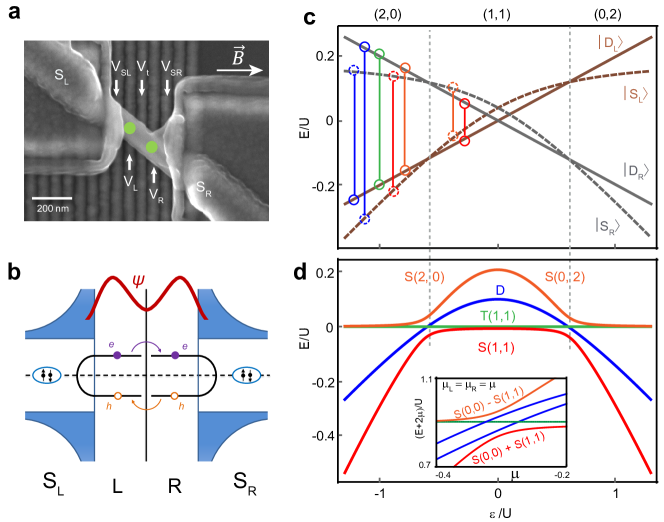
In superconductor-semiconductor hybrid structures, electrons arriving from a semiconductor with energies below the superconducting gap are prohibited from entering the superconductor and are reflected back into the semiconductor as quasiholes via Andreev reflection[26]. Through this mechanism, an electron-hole standing wave, known as an Andreev bound state, can form in the semiconductor (Fig. 1b). In a single quantum dot, Andreev bound state spectrum consists of a spin-singlet state (S) which is a superposition of 0 and 2 electrons on the quantum dot, and two doublet states and , both of which correspond to a single electron on a quantum dot either in the spin up or spin down state. In Fig. 1c, we depict the Andreev spectra of two decoupled quantum dots along the energy level detuning axis, meaning that the electrostatic energies on the two dots are changed in the opposite directions. From negative to positive detuning, the left dot is occupied with 2, 1 and 0 electrons, while the right dot is occupied with 0, 1, and 2. In the (2,0) and (0,2) double dot configurations, singlet states on both dots are lower in energy than doublets. In the (1,1) configuration, doublets are the ground states.
When the two dots are tunnel-coupled, each of the states on one dot will hybridize with each of the states on the other dot (Fig. 1b). The resulting Andreev molecular spectrum is depicted in Fig.1d. The new singlet states are S(0,2), S(2,0) and S(1,1): these three states hybridize at their degeneracy points due to tunnel coupling. The four doublet states hybridized of D(0,1) and D(1,0), D(2,1) and D(1,2) are nearly degenerate at zero field and are designated as D in Fig.1d and are always the excited states. When the chemical potentials and on the left and right dots are tuned along the energy shift axis, such that the double dot can transition from (0,0) to (1,1) configuration. In this case, S(0,0) and S(1,1) are hybridized by superconducting correlations (Fig. 1d(inset)).
A new type of levels appears below the gap in a double quantum dot: the three triplet states (1,1)=, (1,1)= and (1,1)= trace back to the symmetric combinations of single-dot doublet states. T(0,2) and T(2,0) are above the induced gap due to the large orbital energy and thus they do not correspond to bound Andreev states. In experiment, source-drain voltage bias is applied between and , thus the chemical potentials in the two superconductors are experimentally tunable. This influences the Andreev spectra because Andreev levels are pinned to the energy interval of width 2 around the chemical potential (see supplementary information).
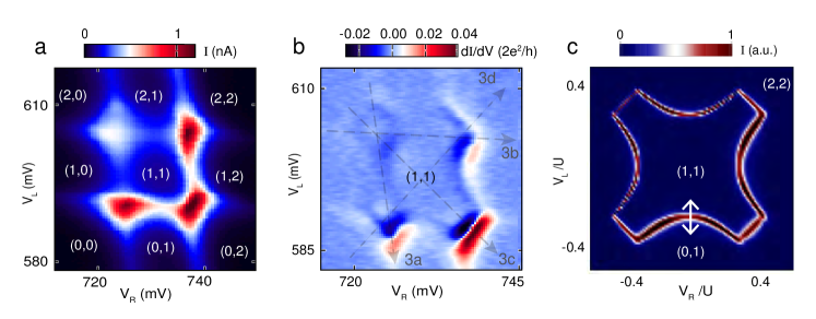
Measurements below are focused on a double dot stability diagram presented in Fig.2a (see supplementary information for expanded diagram). Four degeneracy points are observed at which the current has a local maximum. The upper-left maximum of current is lower than the other three. In reverse , the lower-right maximum has the lowest current. This is due to spin blockade which occurs between (1,1) and (0,2) or (2,0) double dot states due to Pauli exclusion (see supplementary information for further evidence)[27]. Spin blockade is a manifestation of hybridized quantum states on the two dots, and it allows us to identify and label the parity of nine configurations in Fig.2a. The dot occupations are higher than their parities.
In differential conductance the double dot stability diagram is defined by arc-shaped resonances that connect the degeneracy points (Fig.2b). Numerical simulation of transport confirms that these arcs are due to resonances between Andreev states with different double dot configurations. For instance, the resonance between Andreev states in (1,1) and (0,1) yields the lower arc-shaped transport peak depicted in Fig.2c. The same mechanism produces loop-like resonances in gate vs. bias scans (Fig.3). These resonances appear when either dot is fixed at a degeneracy point and the other dot is swept (Fig.3a-b). The similarity between Fig.3a and Fig.3b indicates that the system is symmetric, and Andreev reflection occurs both from the left and the right leads. Loop-like resonances are also observed when the energy levels on the two dots are tuned simultaneously (Fig.3c-d). These resonances are contained within and are accompanied by copies in negative differential conductance.
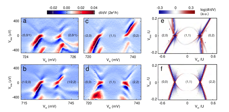
The observed Andreev loops are closed, i.e. the conductance resonances reach zero bias. This is counter-intuitive given that both leads of the system are superconductors and thus an energy gap is expected around zero bias[16, 14]. We ascribe the observed low bias transport to sub-gap quasi-particles that enable single-particle transport. When this effect is included in the numerical model, simulations reproduce the closed loops and negative differential conductance (Figs. 3e-f). We model each lead as being composed of two parts: a conventional superconductor with a hard superconducting gap and a normal Fermi gas with gapless excitations. The electrochemical potentials of the normal and the superconducting parts are pinned together at the value set by the voltage applied to the physical lead. In our model, Andreev reflection off the superconducting part results in the formation of Andreev molecules. The normal part induces transitions between the Andreev molecular states (see supplementary information for details).
We investigate the spin structure of Andreev molecular states by monitoring the evolution of subgap transport features in magnetic field. In Fig. 4a we plot differential conductance as a function of magnetic field and source drain bias for a double quantum dot in the (2,2) configuration. At zero magnetic field we observe two peaks, one at positive bias and one at negative bias. The application of magnetic field results in the splitting of both peaks. Two of the peaks move to higher bias towards the gap edge, while the other pair meets at zero bias. The two merged resonances stick to zero bias at finite field. This effect has been investigated as a signature of Majorana fermions[20]. Here, given the narrow range of field over which the zero-bias peak is observed, we associate it with level repulsion from the gap edge or from other subgap states[19]. By comparing measurements to numerical spectra and transport calculations, we assign the peaks to the transitions between the ground state and the and the excited states (Fig.4b,c). Magneto-transport of the double quantum dot system in the (0,0), (0,2) and (2,0) configurations is qualitatively the same as in the (2,2) configuration (see supplementary information).
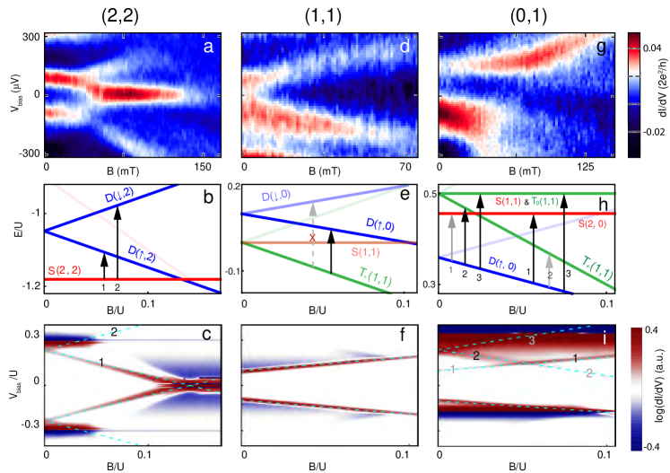
In the (1,1) configuration only a single pair of differential conductance peaks is observed at all fields, one at positive and one at negative bias (Fig. 4d). Both peaks shift to higher bias at higher magnetic fields. The explanation for this behavior originates in the Andreev molecular level structure depicted in Fig. 4e. The low energy manifold consists of ground state that is almost degenerate with the three triplet states , , . At finite field plunges below the and becomes the ground state. Transitions from this triplet state are allowed only to the doublet states , while transitions to are strongly suppressed because they involve an additional spin flip. Both states and shift to lower energies with magnetic field, but the triplet states shifts with while the doublet states shifts with , thus the energy difference between them grows with field. Transport calculations using our detailed model confirm this picture (Fig. 4f).
Odd total parity configurations (0,1), (1,0), (2,1) and (1,2) offer a richer variety of transport behavior (Fig. 4g, and supplementary information). The common features include asymmetry with respect to bias and kinks in the conductance peaks at which the effective g-factor increases. In some regimes we also observe the magnetic-field induced splitting of conductance peaks into as many as three sub-peaks. In Fig. 4h we plot the Andreev molecular spectrum in the (0,1) configuration as a function of magnetic field at zero bias. While is the well-separated ground state at finite field, there are two singlet states ( and ) and two triplet states ( and ) that can contribute to transport (transport via the state requires a spin flip and is therefore suppressed). Numerically computed transport demonstrating both a kink feature as well as the asymmetry with respect to bias, is plotted in Fig. 4i. The model indicates that the origin of the kink feature is that as increases the transition (labeled 2 in Fig. 4h,i) becomes dimmer while the transition (labeled 1 in Fig. 4h,i) becomes brighter. The dimming and brightening of the transitions is associated with proximity to the interdot resonances that occurs at higher bias. The model shows that the origin of the bias asymmetry is a combination of two factors. First, the energies of the Andreev molecular states are bias dependent, as electrons participating in these states are delocalized between the quantum dots and the leads. Second, the gate setting (VL, VR) is asymmetric, meaning such gate setting results in different parities on the two dots.
The nanowires (diameter 100 nm) are grown in the 111 crystal orientation by metalorganic vapor phase epitaxy from gold catalysts, as described in ref.12. Local gate electrodes (pitch 60 nm) are defined by electron beam lithography and electron beam evaporation of Ti(5 nm)/Au (10 nm) on thermal silicon oxide. The gate electrodes are then covered by Atomic layer dposition grown HfO2 (10 nm). Single InSb nanowires are transferred by a micromanipulator. The superconducting contacts are Ti/NbTi/NbTiN (5/5/150 nm). Prior to sputtering the nanowires are passivated in ammonium sulfide to remove the native oxide.
The measurements are performed at 35 mK in a dilution refrigerator. A d.c. voltage bias is applied to the left superconducting lead (SL) and the current from the right superconducting lead (SR) to the ground is measured by a current amplifier. To measure the differential conductance, a standard lock-in technique is used (77 Hz, 5 V).
References
- [1] Georgescu, I. M., Ashhab, S. & Nori, F. Quantum simulation. Rev. Mod. Phys. 86, 153–185 (2014).
- [2] Bloch, I., Dalibard, J. & Nascimbene, S. Quantum simulations with ultracold quantum gases. Nature Phys. 8, 267–276 (2012).
- [3] Blatt, R. & Roos, C. F. Quantum simulations with trapped ions. Nature Phys. 8, 277–277 (2012).
- [4] Houck, A. A., Tureci, H. E. & Koch, J. On-chip quantum simulation with superconducting circuits. Nature Phys. 8, 292–299 (2012).
- [5] Byrnes, T., Kim, N. Y., Kusudo, K. & Yamamoto, Y. Quantum simulation of fermi-hubbard models in semiconductor quantum-dot arrays. Phys. Rev. B 78, 075320 (2008).
- [6] Singha, A. et al. Two-dimensional mott-hubbard electrons in an artificial honeycomb lattice. Science 332, 1176–1179 (2011).
- [7] Barthelemy, P. & Vandersypen, L. M. K. Quantum dot systems: a versatile platform for quantum simulations. Annalen der Physik 525, 808–826 (2013).
- [8] Kitaev, A. Y. Unpaired majorana fermions in quantum wires. Physics-Uspekhi 44, 131 (2001).
- [9] Sau, J. D. & Das Sarma, S. Realizing a robust practical majorana chain in a quantum-dot-superconductor linear array. Nature Communications 3, 964 (2012).
- [10] Fulga, I. C., Haim, A., Akhmerov, A. R. & Oreg, Y. Adaptive tuning of majorana fermions in a quantum dot chain. New Journal of Physics 15, 045020 (2013).
- [11] Zhang, P. & Nori, F. Majorana bound states in a disordered quantum dot chain. New Journal of Physics 18, 043033 (2016).
- [12] Plissard, S. R. et al. From insb nanowires to nanocubes: Looking for the sweet spot. Nano Letters 12, 1794–1798 (2012).
- [13] Eichler, A. et al. Even-odd effect in andreev transport through a carbon nanotube quantum dot. Phys. Rev. Lett. 99, 126602 (2007).
- [14] Eichler, A. et al. Tuning the josephson current in carbon nanotubes with the kondo effect. Phys. Rev. B 79, 161407 (2009).
- [15] Deacon, R. S. et al. Tunneling spectroscopy of andreev energy levels in a quantum dot coupled to a superconductor. Phys. Rev. Lett. 104, 076805 (2010).
- [16] Pillet, J.-D. et al. Andreev bound states in supercurrent-carrying carbon nanotubes revealed. Nature Phys. 6, 965–969 (2010).
- [17] Dirks, T. et al. Transport through andreev bound states in a graphene quantum dot. Nature Phys. 7, 386–390 (2011).
- [18] Chang, W., Manucharyan, V. E., Jespersen, T. S., Nygård, J. & Marcus, C. M. Tunneling spectroscopy of quasiparticle bound states in a spinful josephson junction. Phys. Rev. Lett. 110, 217005 (2013).
- [19] Lee, E. J. et al. Spin-resolved andreev levels and parity crossings in hybrid superconductor-semiconductor nanostructures. Nature nanotechnology 9, 79–84 (2014).
- [20] Mourik, V. et al. Signatures of majorana fermions in hybrid superconductor-semiconductor nanowire devices. Science 336, 1003–1007 (2012).
- [21] Nadj-Perge, S. et al. Observation of majorana fermions in ferromagnetic atomic chains on a superconductor. Science 346, 602–607 (2014).
- [22] Aasen, D. et al. Milestones toward majorana-based quantum computing. Phys. Rev. X 6, 031016 (2016).
- [23] Sherman, D. et al. Hybrid double quantum dots: Normal, superconducting, and topological regimes. arXiv:1605.01865 .
- [24] Karzig, T. et al. Scalable designs for quasiparticle-poisoning-protected topological quantum computation with majorana zero modes. arXiv:1610.05289 .
- [25] Zhang, H. et al. Ballistic majorana nanowire devices. Preprint arXiv: 1603.04069 (2016).
- [26] Blonder, G., Tinkham, M. & Klapwijk, T. Transition from metallic to tunneling regimes in superconducting microconstrictions: Excess current, charge imbalance, and supercurrent conversion. Physical Review B 25, 4515 (1982).
- [27] Nadj-Perge, S. et al. Spectroscopy of spin-orbit quantum bits in indium antimonide nanowires. Phys. Rev. Lett. 108, 166801 (2012).
We thank R. Aguado, A. Akhmerov, S. De Franceschi, E. Lee, V. Liu for valuable discussions. Work is supported by Charles E. Kaufman Foundation (S.M.F. and D. P.), NSF DMR-125296, ONR N00014-16-1-2270 (S. M. F.) and AFOSR FA9550-12-1-0057 (A. D.).
D.C., S.P. and E.B. grew InSb nanowires. Z.S. and M.H. fabricated devices. Z.S. and S.F. performed the measurements and analyzed data. A.T., A.D. and D.P. performed numerical simulations. All authors wrote the manuscript.
Correspondence and requests for materials should be addressed to S.M.F. (email: frolovsm@pitt.edu).
See pages - of supp