Twistronics: Manipulating the Electronic Properties of Two-dimensional Layered Structures through their Twist Angle
Abstract
The ability in experiments to control the relative twist angle between successive layers in two-dimensional (2D) materials offers a new approach to manipulating their electronic properties; we refer to this approach as “twistronics”. A major challenge to theory is that, for arbitrary twist angles, the resulting structure involves incommensurate (aperiodic) 2D lattices. Here, we present a general method for the calculation of the electronic density of states of aperiodic 2D layered materials, using parameter-free hamiltonians derived from ab initio density-functional theory. We use graphene, a semimetal, and MoS2, a representative of the transition metal dichalcogenide (TMDC) family of 2D semiconductors, to illustrate the application of our method, which enables fast and efficient simulation of multi-layered stacks in the presence of local disorder and external fields. We comment on the interesting features of their Density of States (DoS) as a function of twist-angle and local configuration and on how these features can be experimentally observed.
I INTRODUCTION
A few short years after the experimental demonstration of the existence of monolayer graphene Novoselov et al. (2004), many other 2D materials, have been successfully fabricated Ayari et al. (2007); Dean et al. (2010); Mak et al. (2010); Radisavljevic et al. (2011); De et al. (2013). Although single-layer 2D systems have intriguing physical properties, there has also been great interest in developing and understanding artificial heterostructures composed of multiple atomic layers weakly bonded by van der Waals forces Geim and Grigorieva (2013). Mechanical or chemical exfoliation and positioning of one layer on top of another allows for a relative twist between successive layers, which can destroy the alignment and thereby break the translational symmetry in the combined system Cao et al. (2016); Koren et al. (2016). The resulting structures may have commensurate stacking for special orientations, but more generally are incommensurate. This allows for interesting new behavior: studies of bilayer graphene have found clear twist-dependent features in both the electronic density of states and the conductivity Rozhkov et al. (2016); Uchida et al. (2014); at very small twist-angles, a domain-wall phase appears, related to the stacking configuration Woods et al. (2014). Similar effects may occur in TMDC semiconductors, with their band-gaps affected by the substrate and the relative twist-angle orientation Ebnonnasir et al. (2014). Incommensurate structures pose a great challenge to theoretical studies since the standard description of solids with crystalline order, a periodic Bravais lattice and the associated Bloch states of electrons, is entirely absent in the combined system although each layer may still be a perfect 2D crystal.
In the effort to capture the physics of incommensurate systems, a simple approximation is to consider large super-cells that can mimic the incommensurate system; in the case of first-principles calculations like density functional theory (DFT), that can afford relatively small cells, this approximation limits the physical system rather severely to special values of the twist angle Uchida et al. (2014). This leaves important questions unaddressed: Are there distinct physical characteristics that distinguish the incommensurate from the commensurate case? Do the properties of commensurate systems approach the proper limit of the incommensurate systems as the twist-angle is varied?
In the present work we introduce a robust framework for the calculation of the properties of truly incommensurate 2D heterostructures that can address such questions for situations involving arbitrary twists between successive layers. Our method is inspired by previous mathematical works on disordered tight-binding models, which can be classified into two distinct concepts. First, an algebraic treatment of electronic transport in disordered systems Bellissard et al. (1994); Prodan (2012) that allows for a rigorous definition of quantum-mechanical operators in a disordered material. Second, the fact that local tight-binding models create exponentially localized observables, that is, they make it possible to controllably remove finite-size and edge effects from calculations Chen and Ortner (2016). We have already provided a rigorous mathematical discussion of this method Massatt et al. (2016), but here investigate its implications and results for physical systems. Our modeling is based on effective tight-binding hamiltonians without any adjustable parameters, obtained from first-principles DFT results Fang and Kaxiras (2016); Fang et al. (2015). As a demonstration of the capabilities of the method, we study some prototypical systems of 2D stacked layers, including bilayer graphene, a semimetal, and bilayer MoS2, a representative semiconductor of the TMDC family.
II FORMALISM
The essence of our approach consists of the following ideas: A tight-binding model in -dimensions is described by localized orbitals in a -dimensional lattice, , and the hopping matrix elements between them labeled . To describe disorder in this model, we consider the space of all possible defects and calculate physical properties for a carefully chosen subset of configurations. This is formulated by defining a configuration space with specific local configurations with a probability distribution . describes all possible environments that an atom in the infinite crystal can experience, and we simulate physical observables by sampling over this space of disordered configurations. This is in contrast to periodic approaches, which instead use the Bloch wavenumber, , as the sampling space. In incommensurate systems translational symmetry has been completely broken, and there is no Brillouin zone. , referred to as the “non-commutative Brillioun zone” for this reason Bellissard et al. (1994), is an alternative to this notion; neither nor the Brillioun zone provide a diagonalized band structure with a finite number of eigenvalues at each point.
Viewing the interlayer interaction as a perturbative potential, the relative twist-angle can be interpreted as an aperiodic disorder field applied to the single-layer system. For a fixed twist angle, the location of the orbital in the field created by another layer varies. This variation in location can be completely described by the offset, or shift, between the two layers’ unit cells, and thus can be viewed as the compact two-dimensional space of all shifts. For each shift, we construct a system of finite radius which contributes a finite-size error. The error decays exponentially with the radius, so it can be made to approach zero in a controlable fashion. Our results prove that this is a computationally feasible strategy.
In this picture, the difference between an incommensurate and commensurate twist angle becomes trivial: a commensurate angle has a finite number of possible configurations because a periodic super-cell exists, while an incommensurate angle has an infinite number. If two twist angles, commensurate and incommensurate, are extremely close then a specific shift configuration will look effectively identical between them. Therefore, the results of a single calculation will not vary significantly between and ; rather, it is the sampling of that varies. For the twist angle to act as the order parameter in a phase transition between commensurability and incommensurability, a physical observable must vary strongly enough over and the commensurate twist angle must not sample too finely. This distinction only holds for each layer being a perfect infinite crystal. In real materials, the difference between an incommensurate and a commensurate twist-angle is less clear, as the presence of imperfections (strain, tears, ripples) may make even a commensurate system sample continuously.
Our approach can also handle other sources of disorder straightforwardly. Magnetic and electric fields can be easily introduced through a Peierl’s substitution or an on-site energy term, respectively. Physical defects such as vacancies, ripples, and edges are easy to implement, provided that it has been established how the hopping terms of the tight-biding hamiltonian change in the presence of defects. This is handled by introducing extra dimensionality to to represent all possible forms of disorder and applying them directly in each tight-binding model.
Our implementation of these ideas on a high-performance computing system are as follows:
i) Creation of a heterostructure model out of layers that are disks of radius ; these
disks are centered at a point with “zero-shift”,
which is just one specific configuration.
ii) Determination of all relevant hopping indices
in the sparse hamiltonian by only looking for pairs of orbitals
that are within the range of the hopping matrix elements .
iii) For each desired configuration ,
displacement of one layer by the some amount
with respect to the other layer,
and computation of for each non-zero hopping term;
from this, we then calculate the local electronic density of states (LEDoS), or any
other useful physical property like the conductivity.
The LEDoS is derived from the global EDoS, ,
by considering all eigenstates (indexed by ) and orbitals (indexed by ):
| (1) |
iv) Application of the operator of interest to with a Kernel Polynomial Method (Chebyshev polynomials) Weiß e et al. (2006); Di Napoli et al. (2016); the Chebyshev polynomials form a complete basis for square integrable functions which take values in the range and a linear combination of them can be chosen to approximate the eigenspectrum of a tight-binding hamiltonian after a simple rescaling to ensure all eigenvalues lie in .
An additional advantage of the method is that it can be formulated into a code with excellent parallel efficiency, especially compared to DFT super-cell calculations. This is a consequence of the fact that to obtain the global operator requires a large number of independent computations of the local operator in different configurations that can be run in parallel (we use MVAPICH 2.2b). Since each local operator is computed using only sparse matrix-vector operations, a second layer of parallelization can be added by using multi-threaded implementations of highly optimized matrix-vector operator subroutines, which further enhances efficiency (we use Intel MKL 11.0).
III BILAYER GRAPHENE
Twisted bilayer graphene (tBLG) provides an excellent candidate for a test of our method, since it has been well characterized by many experimental works and analytical theory Bistritzer and MacDonald (2011); San-Jose et al. (2012). To compute the EDoS of tBLG we used a two-band model that describes the bonding and antibonding combinations of orbitals associated with the two-atom basis of the honeycomb lattice; the tight-binding hamiltonian is derived from first-principles calculations with the use of Wannier orbitals and involves no adjustable parameters, other than the range of hopping matrix elements Fang and Kaxiras (2016).
The main feature of twisted bilayer graphene is the presence of van Hove singularities (VHS) above and below the Fermi energy. The origin of these VHS can be best understood by considering the low-energy band-structure of tBLG as consisting of four Dirac cones at the valleys and , where labels the layers. At twist, and are at the same point in momentum-space. For , the Dirac cones move away from one another in momentum-space, and a partial band-gap opening occurs where the cones now overlap. These hybridizations at the overlap of the Dirac cones produce the VHS Castro Neto et al. (2009), which have already been investigated by experimental STM measurements Li et al. (2009); Luican et al. (2011); Wong et al. (2015); Yin et al. (2015).
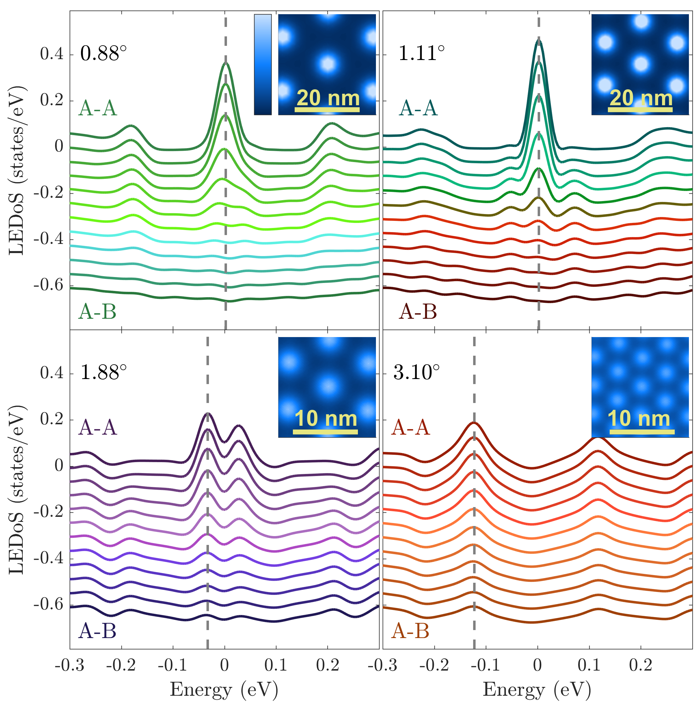
As a first test of the method, in Fig. 1 we compare the spatial dependence of tBLG at four twist angles to experimental results Yin et al. (2015). This is possible because sampling shifts over the diagonal of one layer’s unit-cell is the same as moving linearly from an AA to AB type stacking in the real-space moiré pattern. For these calculations we use a disk cut-off radius Å which contains atoms. The simulated features of the VHS for the four selected angles are identical to those from experiment Yin et al. (2015), but the scaling between the VHS feature and the background graphene DoS are different between theory and experiment. This can be partly explained by the fact that in STM measurements states with lower in-plane momentum have shorter decay lengths Stroscio et al. (1986); Huang et al. (2015). Our method gives the DoS independent of the momentum of electronic states that contribute to it, so it is expected that the VHS will be less pronounced in experiment.
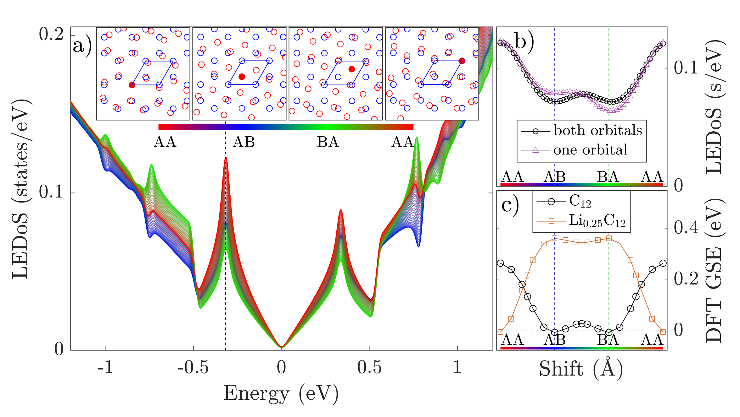
Next, we sample the configuration space for a fixed twist angle of (0.1 radians) for 100 configurations along the diagonal of the unit-cell, see Fig. 2. The LEDoS varies smoothly as a function of , with the only regions of significant configuration dependence being those near the VHS. The AB (BA) type stacking has much lower DoS at the VHS than any other stacking configuration. Since we fit the DoS to a smooth polynomial, the divergent nature of the DoS at the VHS is only partially recovered. We can still compare the intensity of the VHS by examining its spectral weight. In Fig. 2 (c) we plot the DFT ground-state energy calculations for non-twisted bilayer graphene over the same range of relative shifts. There are interesting similarities between the VHS LEDoS and the ground-state energy, namely, the LEDoS at the VHS has the same dependence on relative shift as the energy. An important question is: can one controllably induce a relative twist between two graphene layers in samples of macroscopic size? We suggest that use of intercalants may facilitate this process. In particular, Li-ions are know to be easily intercalated between graphene layers, with both insertion and removal being fast processes. Inspired by this observation, we have also calculated the ground-state energy as a function of relative shift for a graphene bilayer including Li-ion intercalation. In the fully lithiated structure, the relative stability of the AB and AA stacking is inverted, suggesting that Li-ion intercalation may indeed act as a way to facilitate changes in the relative twist-angle even for macroscopic samples.
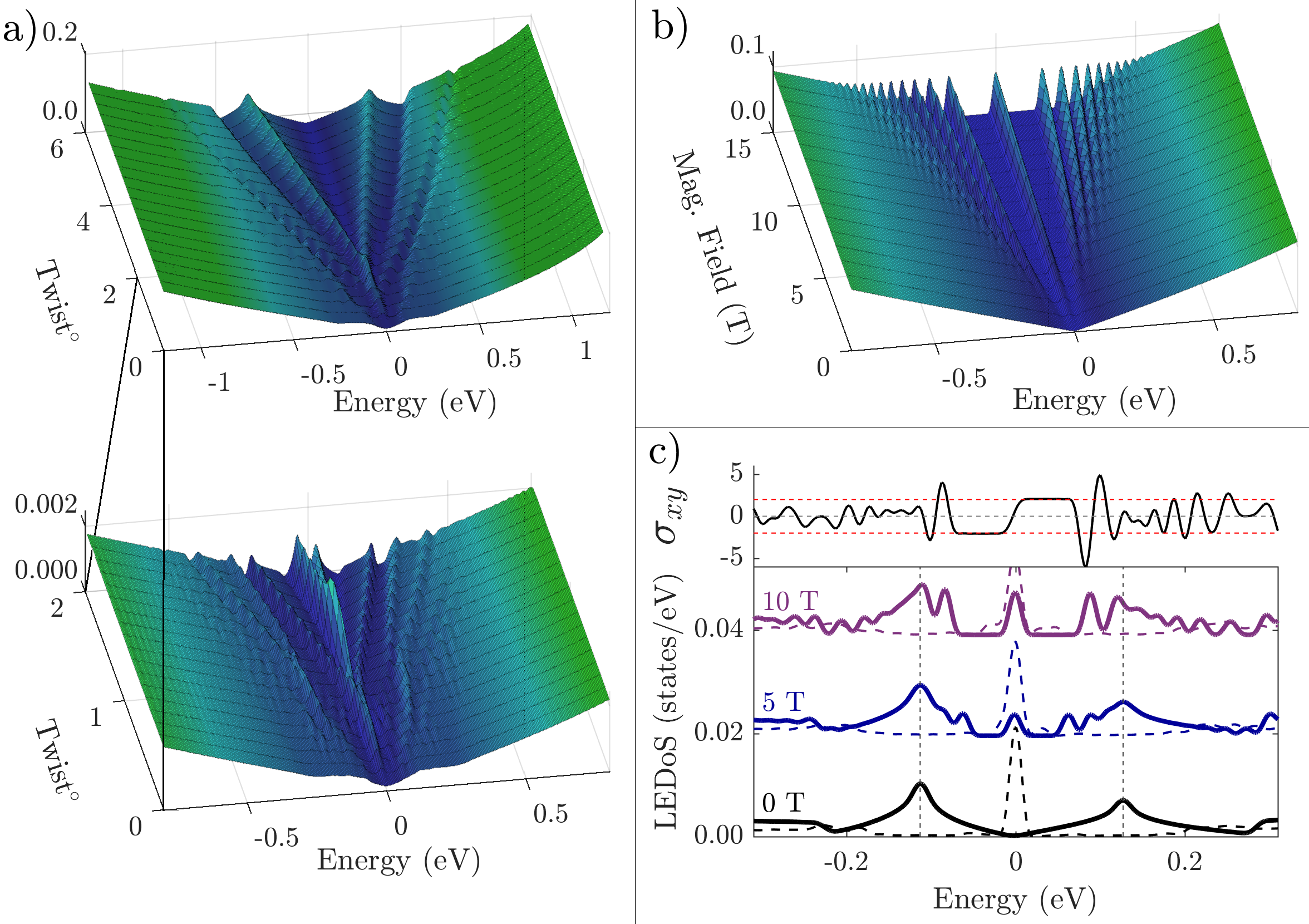
In Fig. 3(a) we plot the angle-dependent EDoS for tBLG. The first, second, and third VHS are visible in the low-angle regime and they move away from the Fermi level linearly with twist angle. At the VHS, we find that the real-space local DoS is highly localized at the AA stacking sites as in Fig. 1, in agreement with experimental STM results Wong et al. (2015); Brihuega et al. (2012). It is easy to identify in Fig. 3(a) the first and second “magic angles” of tBLG (near and , respectively), explained by band flattening near the Fermi level Bistritzer and MacDonald (2011); San-Jose et al. (2012). In Fig. 3(b) we plot the calculated EDoS of monolayer graphene in the presence of out-of-plane magnetic field. The Landau levels (LL’s) in the monolayer and the VHS in the twisted bilayer both represent tunable, localized electronic states, supporting the interpretation of the interlayer interaction in a twisted heterostructure as a non-abelian gauge field San-Jose et al. (2012); Yin et al. (2015). These calculations allow a very robust determination of the monolayer’s Fermi velocity without a band-structure calculation, using the low-energy model for the LL’s Castro Neto et al. (2009)
| (2) |
with the result for the Fermi velocity m/s. Finally, we test the interaction between twist and magnetic field in Fig. 3(c): at the AA stacking with a twist there are many clear LL’s and at a field of 5 T, the peak of the VHS is significantly altered relative to its zero-field shape. At a twist of , the magnetic field dependence of the peak is not visible. These results are in good agreement with experimental STM measurements Luican et al. (2011); Yin et al. (2015).
The Str̈eda formula Streda (1982) relates the fluctuations in the integrated electronic density under small changes in the magnetic field strength to the Hall conductance , while the energy of the system energy is in an energy-gapped region, :
| (3) |
Averaging over 100 configurations of the LEDoS on both layers with a 750 Å cut-off radius ( atoms), gives values for that jump from to in units of across the central LL in the simulation. This change of , before taking into account spin, corresponds to the four-fold degeneracy for the LL of bilayer graphene, with the four states originating from the monolayer’s valley degeneracy (factor of 2) and the two sheets (another factor of 2). A change of is observed in experiment for tBLG, which is in agreement with our results when we take into account spin degeneracy Cao et al. (2016). If only the AA configuration is used in the calculation we do not obtain good quantization of . Just like integrating over the entire Brillouin Zone when computing in momentum space, integrating over the entire configuration space is required in the case of tBLG. This allows us to compute the Chern number for the wavefunctions in the gapped region by taking the difference in in units of the conductance quanta (), which indicates that our method can capture accurately certain topological properties of the electronic band structure.
IV BILAYER TMDC
Unlike bilayer graphene, transition metal dichalcogenides will not be well described by low-energy theory due to their large band-gaps (about 2 eV). For bilayers of TMDCs we use an 11 band model, consisting of 5 orbitals on the transition metal atom and 3 orbitals on each of the two chalcogen atoms Fang et al. (2015). The interlayer interaction is modeled only between the chalcogen atoms closest to the bilayer interface. Here we present results for MoS2, whose model hamiltonian includes GW corrections for more accurate representation of the electronic structure. Since we are mainly interested in studying twist-angle dependent effects, we will neglect spin polarization, but an ab-initio model with spin-orbit coupling can be easily substituted if such effects are important.
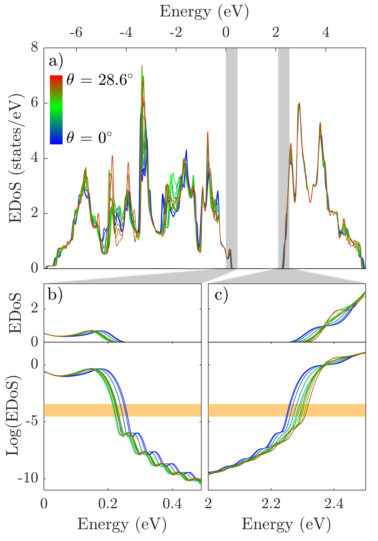
Some twist-angle dependent features were seen in the LEDoS for both WSe2 and MoS2, but most were not near the conduction or valence band-edges. The twist-angle dependence of the density of states for bilayer MoS2 is shown in Fig. 4(a). These calculations were performed with a 300 Å cut-off radius ( atoms) and averaged over 100 configurations. There are significant changes in the EDoS deep into the valence band (more than 2 eV below the maximum), but it is difficult to probe this region experimentally. They could be observed as interesting properties for high-frequency conductivity or optical activity.
Instead, we focus on the valence and conduction band edges. The band-gap is a twist-angle dependent feature: it increases by 76 meV (a % change) going from to twist-angle. The regions near the valence and conduction band extrema are shown in great detail in Fig. 4(b) and (c), with the logarithmic scale showing the changes more clearly. These plots also show the good numerical convergence of the EDoS in our model, with noticeable numeric error only occurring when the EDoS is smaller than states per eV. This error, reminiscent of Gibbs oscillations Weiß e et al. (2006), is likely an artifact of the KPM attempting to fit a smooth function to a band-edge in the eigenvalue spectrum. We thus take a region about states per eV to compare changes in the band-gap (plotted in orange). Our model does not take into account changes in the distance between the two layers as a function of twist-angle, which could give additional dependence of the band-gap and can be incorporated as a dependence of the tight-binding hopping matrix elements on twist angle and distance.
V CONCLUSION
We have introduced a new method for parameter-free computation of electronic properties in incommensurate layered 2D materials with controllable errors. Although here we have only studied bilayer materials, the method is general and extends to any number of layers and of arbitrary heterostructure composition. Viewing the problem on the space of configurations, , allows us to fully characterize the properties of incommensurate (aperiodic) systems. The method allows for the inclusion of external fields and other sources of disorder, such as strain or defects. We present results of applying the method to twisted bilayer graphene and a representative of the TMDC family of semiconductors. The method is accurate enough to correctly calculate quantization of Hall conductivity in tBLG in the presence of magnetic fields, and reproduces the correct Chern number for the Landau Level. It also predicts that bilayer TMDC’s have a twist-dependent band-gap. The method is a promising candidate for the targeted design of electronic properties in layered heterostructures.
Acknowledgements.
We acknowledge S. Shirodkar for providing the Li-ion itercalated graphene calculations shown in Fig. 2(c) and B.I. Halperin and D. Huang for helpful discussions. The computations in this paper were run on the Odyssey cluster supported by the FAS Division of Science, Research Computing Group at Harvard University. This work was supported by the ARO MURI Award No. W911NF-14-0247. SF is supported by the STC Center for Integrated Quantum Materials, NSF Grant No. DMR-1231319.References
- Novoselov et al. (2004) K. S. Novoselov, A. K. Geim, S. V. Morozov, D. Jiang, Y. Zhang, S. V. Dubonos, I. V. Grigorieva, and A. A. Firsov, Science (New York, N.Y.) 306, 666 (2004).
- Ayari et al. (2007) A. Ayari, E. Cobas, O. Ogundadegbe, and M. S. Fuhrer, Journal of Applied Physics 101, 014507 (2007).
- Dean et al. (2010) C. R. Dean, a. F. Young, I. Meric, C. Lee, L. Wang, S. Sorgenfrei, K. Watanabe, T. Taniguchi, P. Kim, K. L. Shepard, and J. Hone, Nature nanotechnology 5, 722 (2010).
- Mak et al. (2010) K. F. Mak, C. Lee, J. Hone, J. Shan, and T. F. Heinz, Physical review letters 105, 136805 (2010).
- Radisavljevic et al. (2011) B. Radisavljevic, A. Radenovic, J. Brivio, V. Giacometti, and A. Kis, Nature nanotechnology 6, 147 (2011).
- De et al. (2013) D. De, J. Manongdo, S. See, V. Zhang, A. Guloy, and H. Peng, Nanotechnology 24, 025202 (2013).
- Geim and Grigorieva (2013) A. K. Geim and I. V. Grigorieva, Nature 499, 419 (2013).
- Cao et al. (2016) Y. Cao, J. Y. Luo, V. Fatemi, S. Fang, J. D. Sanchez-Yamagishi, K. Watanabe, T. Taniguchi, E. Kaxiras, and P. Jarillo-Herrero, Physical Review Letters 117, 116804 (2016).
- Koren et al. (2016) E. Koren, I. Leven, E. Lörtscher, A. Knoll, O. Hod, and U. Duerig, Nature nanotechnology 11, 752 (2016).
- Rozhkov et al. (2016) A. Rozhkov, A. Sboychakov, A. Rakhmanov, and F. Nori, Physics Reports 648, 1 (2016).
- Uchida et al. (2014) K. Uchida, S. Furuya, J.-I. Iwata, and A. Oshiyama, Physical Review B 90, 155451 (2014).
- Woods et al. (2014) C. R. Woods, L. Britnell, A. Eckmann, R. S. Ma, J. C. Lu, H. M. Guo, X. Lin, G. L. Yu, Y. Cao, R. V. Gorbachev, A. V. Kretinin, J. Park, L. A. Ponomarenko, M. I. Katsnelson, Y. N. Gornostyrev, K. Watanabe, T. Taniguchi, C. Casiraghi, H.-J. Gao, A. K. Geim, and K. S. Novoselov, Nature Physics 10, 451 (2014).
- Ebnonnasir et al. (2014) A. Ebnonnasir, B. Narayanan, S. Kodambaka, and C. V. Ciobanu, Applied Physics Letters 105, 031603 (2014).
- Bellissard et al. (1994) J. Bellissard, A. van Elst, and H. Schulz- Baldes, Journal of Mathematical Physics 35, 5373 (1994).
- Prodan (2012) E. Prodan, Applied Mathematics Research eXpress 2, 176 (2012).
- Chen and Ortner (2016) H. Chen and C. Ortner, SIAM Multiscale Model. Simul. 14, 232 (2016).
- Massatt et al. (2016) D. Massatt, M. Luskin, and C. Ortner, (unpublished) , 1 (2016), arXiv:1608.01968 .
- Fang and Kaxiras (2016) S. Fang and E. Kaxiras, Physical Review B 93, 235153 (2016).
- Fang et al. (2015) S. Fang, R. Kuate Defo, S. N. Shirodkar, S. Lieu, G. a. Tritsaris, and E. Kaxiras, Physical Review B 92, 205108 (2015).
- Bistritzer and MacDonald (2011) R. Bistritzer and A. H. MacDonald, Proceedings of the National Academy of Sciences of the United States of America 108, 12233 (2011).
- San-Jose et al. (2012) P. San-Jose, J. González, and F. Guinea, Physical review letters 108, 216802 (2012).
- Castro Neto et al. (2009) a. H. Castro Neto, F. Guinea, N. M. R. Peres, K. S. Novoselov, and a. K. Geim, Reviews of Modern Physics 81, 109 (2009).
- Li et al. (2009) G. Li, A. Luican, J. M. B. Lopes dos Santos, a. H. Castro Neto, A. Reina, J. Kong, and E. Y. Andrei, Nature Physics 6, 109 (2009).
- Luican et al. (2011) A. Luican, G. Li, A. Reina, J. Kong, R. R. Nair, K. S. Novoselov, a. K. Geim, and E. Y. Andrei, Physical review letters 106, 126802 (2011).
- Wong et al. (2015) D. Wong, Y. Wang, J. Jung, S. Pezzini, A. M. DaSilva, H.-Z. Tsai, H. S. Jung, R. Khajeh, Y. Kim, J. Lee, S. Kahn, S. Tollabimazraehno, H. Rasool, K. Watanabe, T. Taniguchi, A. Zettl, S. Adam, A. H. MacDonald, and M. F. Crommie, Physical Review B 92, 155409 (2015).
- Yin et al. (2015) L.-J. Yin, J.-B. Qiao, W.-J. Zuo, W.-T. Li, and L. He, Physical Review B 92, 081406 (2015).
- Stroscio et al. (1986) J. Stroscio, R. Feenstra, and A. Fein, Physical review letters 57, 2579 (1986).
- Huang et al. (2015) D. Huang, C.-L. Song, T. a. Webb, S. Fang, C.-Z. Chang, J. S. Moodera, E. Kaxiras, and J. E. Hoffman, Physical review letters 115, 017002 (2015).
- Brihuega et al. (2012) I. Brihuega, P. Mallet, H. González-Herrero, G. Trambly de Laissardière, M. M. Ugeda, L. Magaud, J. M. Gómez-Rodríguez, F. Ynduráin, and J.-Y. Veuillen, Physical review letters 109, 196802 (2012).
- Streda (1982) P. Streda, Journal of Physics C: Solid State Physics 15, 1299 (1982).
- Weiß e et al. (2006) A. Weiß e, G. Wellein, A. Alvermann, and H. Fehske, Reviews of Modern Physics 78, 275 (2006).
- Di Napoli et al. (2016) E. Di Napoli, E. Polizzi, and Y. Saad, Numerical Linear Algebra with Applications 23, 674 (2016).