Electronic and optical properties of two-dimensional InSe
from a DFT-parameterized tight-binding model
Abstract
We present a tight-binding (TB) model and theory for electrons in monolayer and few-layer InSe. The model is constructed from a basis of all and valence orbitals on both indium and selenium atoms, with tight-binding parameters obtained from fitting to independently computed density functional theory (DFT) band structures for mono- and bilayer InSe. For the valence and conduction band edges of few-layer InSe, which appear to be in the vicinity of the point, we calculate the absorption coefficient for the principal optical transitions as a function of the number of layers, . We find a strong dependence on of the principal optical transition energies, selection rules, and optical oscillation strengths, in agreement with recent observations Bandurin et al. (2016). Also, we find that the conduction band electrons are relatively light (), in contrast to an almost flat, and slightly inverted, dispersion of valence band holes near the -point, which is found for up to .
I Introduction
Two-dimensional (2D) crystals are atomically thin films of van der Waals materials that are stable when exfoliated from the three-dimensional crystal due to the weak nature of the interaction holding the individual layers togetherYoffe (1973). Examples of such materials include graphiteNovoselov et al. (2005), boron nitrideGorbachev et al. (2011), and transition metal dichalcogenidesMak et al. (2010), which have shown that properties of monolayer and bilayer crystals may strongly differ from the bulk properties of these layered compounds. Many of the transition metal dichalcogenides have been shown to possess optical properties that make them well suited for use in photodetectors and other optical or optoelectronic applicationsSplendiani et al. (2010); Korn et al. (2011); Wang et al. (2012); Xu et al. (2014); Jones et al. (2013); Gan et al. (2013); Wu et al. (2014); Sie et al. (2015); Wang et al. (2015); Liu et al. (2015).
Another chalcogenide currently emerging as a high potential material for use on optical applications is the layered hexagonal metal chalcogenide InSe, atomically thin films of which are possible to fabricateLei et al. (2014); Mudd et al. (2013, 2014, 2015); Tamalampudi et al. (2014); Balakrishnan et al. (2014). While in its bulk form InSeDamon and Redington (1954); Likforman et al. (1975); Williams et al. (1977); Manjón et al. (2004, 2001); Pellicer-Porres et al. (1999); Goi et al. (1992); Kress-Rogers et al. (1982); Gorshunov et al. (1998); Dmitriev et al. (1995); Millot et al. (2010); Segura et al. (1983, 1997); McCanny and Murray (1977); De Blasi et al. (1983) is a direct gap semiconductor Camassel et al. (1978a), its electronic structure undergoes significant changes upon exfoliation to few-layer or monolayer thickness, with particularly interesting optical properties observed in recent experimentsBandurin et al. (2016); Mudd et al. . Density functional theory (DFT) calculations for single layer crystals of InSeZólyomi et al. (2014); Rybkovskiy et al. (2014) predict a large increase in the band gap as compared to bulk crystals, with the valence band maximum slightly shifted from the point. Despite being a van der Waals layered material, bulk InSe has a light effective mass for electrons in the conduction and valence band across the layers. Therefore, it is expected that the band gapZólyomi et al. (2014); Mudd et al. (2014); Sun et al. (2016) and related physical properties of few-layer InSe will exhibit a strong dependence on the number of layers.
In this work we develop a tight-binding (TB) model of atomically thin InSe, tracing the dependence of electronic and optical properties on the number of layers () in the film. We use density functional theory (DFT) to parametrize the model and apply a scissor correction to compensate for the underestimation of the band gap. Indeed, we find that as compared to the majority of other layered materials with van der Waals coupling between consecutive layers, which have the out-of-plane electron mass heavier than the in-plane mass, in InSe this relation is reversed leading to a strong -dependence of the band gap. Also, the stacking of consecutive layers in few-layer -InSe similar to A-B-C stacking in graphite breaks the mirror-plane symmetry of monolayer InSe, which should be expected to affect optical selection rules and SO coupling in few-layer InSe.
We use the TB model developed here to predict the band structure of few-layer InSe, and we develop a model to predict the optical properties, with the matrix elements of the momentum operator obtained from the TB model. We provide estimates for the band edge optical absorption coefficient as a function of the number of layers. The paper is structured as follows.
In Section II we discuss the crystal structure of InSe. In Section III we present the model of monolayer InSe and in Section IV we expand it to bilayer InSe. In Section V we apply the model to few-layer InSe. In Section VI we present a 4-band theory model, and we calculate the momentum matrix elements and the band edge optical absorption in few-layer InSe, which enables us to interpret the recent experimental results in Ref.Bandurin et al., 2016. The theory in section VI also describes spin-orbit coupling terms in mono- and few-layer InSe.
II Crystal Structure and symmetry
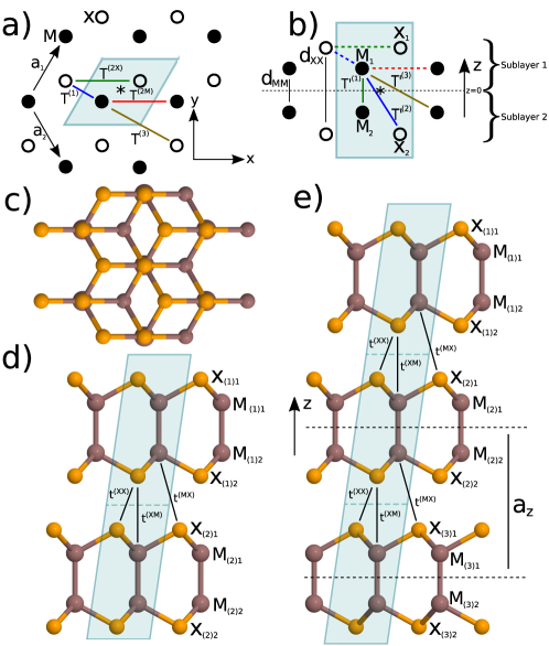
The crystalline structure of monolayer InSe considered in this study takes the form of hexagonal III-VI chalcogenides in M2X2 stoichiometry, where M is a metal atom of group III and X is a chalcogen atom of group VI. The structure is illustrated in Fig. 1a-c. A unit cell of the monolayer consists of four ions - one metal and one chalcogen in each of two sublayers.
The monolayer crystal has point-group symmetry (see Fig. 2) which includes mirror symmetry (, or reflection). This symmetry operation effectively swaps the sublayers. From a top-down view, the crystal exhibits a honeycomb structure in the plane, where sites are occupied by metal ions and sites by chalcogen ions, possessing rotational symmetry centered at each atomic position (, or rotation) and mirror symmetry (, or reflection) in the plane (and equivalent planes generated by ). The Bravais lattice is given by
| (1) | ||||
where and are integers, and the full crystal structure is given by
| (2) | ||||
where is a In/Se atom in the top (bottom) sublayer. The structure of -InSe is shown in Fig. 1e. The monolayers are stacked such that chalcogen atoms in the top layer are directly above the metal atoms in the layer below, while the chalcogen atoms in the bottom layer are not directly below the metal atoms in the layer above. The vector between a chalcogen atom and the metal atom directly below it is
| (3) |
while the vectors between a chalcogen atom and the nearest chalcogen atoms in the layer below are
| (4) |
where (=1,2,3) are the vectors between nearest-neighboring M-X pairs in the top sublayer of a monolayer. 8.32 Å is the distance along between the central plane of each layer. The structure parameters for monolayer InSe are given in the caption of Fig. 1.
It is important to note here that, due to the stacking, the point symmetry of the material is reduced from that of the monolayer. Bulk and few-layer -InSe exhibit only symmetry while in the monolayer we have symmetry. The main difference between the two cases is that the symmetry of the monolayer is broken by the stacking when we have more than one layer; this has important consequences for the optical matrix element, which is discussed below. In the bulk adjacent monolayers are related by and screw axes along . The space group symmetry for the bulk crystal is .
III TB model for monolayer InSe
III.1 Hamiltonian
To describe InSe in a TB model, we construct our basis from the and orbitals of In (group III) and Se (group VI) atoms, and consider all possible hoppings between these orbitals up to second-nearest neighbor interactions. The Hamiltonian takes the form
| (5) |
where the sum over runs over the sublayers in the model, and when . Here, contains terms arising from the on-site energies of the orbitals, while and describe the hopping interactions within and between the sublayers, respectively, detailed below. Motivated by the dominant orbital contributions in DFT data for bands with energies near the Fermi level, we start from an atomic orbital basis including and orbitals in the valence shells of and atoms. takes the form
| (6) | ||||
where the sum in goes over all unit cells in the crystal, while . Parameters and are on-site energies for the orbitals of metal and chalcogen ions respectively, while and are on-site energies for the relevant orbitals. is the annihilation (creation) operator for an electron in orbital on ion in unit cell . , is an annihilation (creation) operator for a orbital.
contains the hopping terms arising from intra-sublayer interactions, and is formed of the contributions
| (7) |
where includes nearest-neighbor hoppings for M-X pairs (labeled T(1) in Fig. 1), while and include hoppings for nearest pairs of like ions (M-M and X-X), (labeled T(2M) and T(2X)), and includes hoppings between next-nearest M-X pairs (labelled T(3)). The contributions are
| (8) | ||||
| (9) | ||||
| (10) | ||||
| (11) | ||||
where the sum over is over nearest-neighboring M-X pairs within a sublayer, and , , and are over nearest M-M, X-X and next-nearest M-X pairs respectively. In considering the hoppings between the various and orbitals we have made the two-center approximation, as set out by Slater and Koster Slater and Koster (1954). is the hopping integral for nearest-neighboring orbitals, and take into account hopping, while is the component of hopping where the orbitals are parallel to each other and perpendicular to the vector between the ions (hopping vector) and is the hopping between the components of the orbitals lying along the hopping vector. takes account of the component of a orbital along the hopping vector, and thus has the form
| (12) |
where is a unit vector along .
The inter-sublayer hopping is written as
| (13) |
where
| (14) | ||||
| (15) | ||||
| (16) | ||||
III.2 DFT band structures of monolayer and bulk InSe and parametrization of monolayer TB model
The DFT data to which we fit and compare the TB model of InSe in this section are obtained using the LDA exchange-correlation functional as set out in Ref. Zólyomi et al., 2014 for In2X2 materials. In these calculations the VASP codeKresse and Furthmüller (1996) is used to describe the materials in a plane-wave basis. The cutoff energy for the plane-wave basis is 600 eV and the vertical separation between repeated images of the monolayer is set to 20 Å to ensure that any interactions between them would be negligible. The Brillouin zone is sampled by a -point grid.
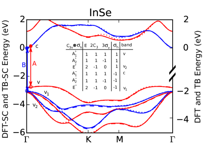
As semilocal density functional theory underestimates the band gap, we apply the “scissor” correction to the DFT energy gaps, as employed before in the studies of other semiconductors Fiorentini and Baldereschi (1995); Johnson and Ashcroft (1998); Bernstein et al. (2002); Parashari et al. (2008); Thilagam et al. (2010); Babu et al. (2011), as follows. A calculation with the LDA returns the band gap for bulk InSe as 0.41 eV as compared to the bulk experimental value of 1.40 eV at low temperature Camassel et al. (1978b); Millot et al. (2010) (1.25 eV at room temperature Mudd et al. (2013)). Hence, we subtract eV from the energies of all valence band states while keeping the conduction band energies unchanged for bulk, few-layer, and monolayer InSe. For optics, this scissor correction is equivalent to adding to the energies of all interband transitions (labeled and in Fig. 2), which we identify upon analyzing wave functions in the bands of monolayer and few-layer InSe (at room temperature, we use eV).
In the following we fit the TB model to the scissor corrected DFT band structure, and call this scissor corrected tight-binding (TB-SC). We do this by applying a constrained least squares minimization procedure to the difference between the TB and the scissor corrected DFT band energies. While the procedure is in principle straightforward, in practice one must take care, in particular with the choice of bands to use for the fitting procedure. For comparison, we also perform a fit to the original DFT data to obtain a parametrization without scissor correction (TB).
On diagonalization the model yields 16 bands – 8 even (symmetric) and 8 odd (antisymmetric) under . As one progresses further in energy away from the conduction band edge and valence band edge the assumption that and orbital contributions dominate begins to break down, with significant orbital contributions at energies far away from the band edges. In addition, the DFT calculation is less accurate in the higher energy unoccupied bands. We therefore fit the model to 7 DFT bands - the 5 highest energy valence bands (3 even, 2 odd) and the 2 lowest energy conduction bands (1 even, 1 odd), using bands 3-6 of the 8 even model bands, and bands 3-5 of the odd model bands. As our primary purpose is a good quantitative fit to the valence and conduction band edges, we give extra weights to these points during the fitting procedure. The fit is carried out over a grid of 141 points in -space covering the irreducible portion of the Brillouin zone.
Table 1 presents the parameters obtained in the fit for InSe with scissor correction taken into account (TB-SC) and without it (TB) for sake of completeness. Fig. 2 shows the TB band structure (TB-SC) and the DFT data (DFT-SC) to which the fit was applied for InSe; the TB band structure without scissor correction (TB) is also plotted in comparison to the raw DFT data (DFT). The model gives a good reproduction of the DFT bands, both with and without scissor correction. Note that slight differences can be found between the shape of the fitted bands when comparing the fit to the raw DFT data and the scissor corrected bands, and the parameter sets differ accordingly.
| TB-SC | TB | |
| -7.174 | -7.595 | |
| -2.302 | -3.027 | |
| 1.248 | 0.903 | |
| -14.935 | -15.188 | |
| -7.792 | -8.045 | |
| -7.362 | -7.615 | |
| 0.168 | 0.331 | |
| 2.873 | 2.599 | |
| -2.144 | -2.263 | |
| 1.041 | 0.977 | |
| 1.691 | 1.342 | |
| -0.200 | -0.248 | |
| -0.137 | -0.113 | |
| -0.433 | -0.561 | |
| -1.034 | -1.130 | |
| -1.345 | -1.451 | |
| -0.800 | -0.843 | |
| -0.148 | -0.110 | |
| -0.554 | -0.613 | |
| 0.821 | 0.793 | |
| 0.156 | 0.179 | |
| -0.294 | -0.323 | |
| 0.003 | -0.015 | |
| -0.455 | -0.477 | |
| -0.780 | -0.518 | |
| -4.964 | -4.644 | |
| -0.681 | -0.769 | |
| -4.028 | -4.052 | |
| 0.574 | 0.472 | |
| -0.651 | -0.544 | |
| -0.148 | -0.138 | |
| 0.100 | 0.082 | |
| 0.343 | 0.373 | |
| -0.238 | -0.187 | |
| -0.048 | -0.065 | |
| -0.020 | -0.052 | |
| -0.151 | -0.168 |
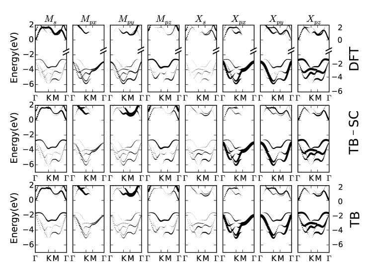
Alongside the energies predicted by our model Hamiltonian, it is useful to check the orbital decomposition, found in the normalized eigenvectors, against that given by the DFT results. We define as the coefficient of the eigenfunction of band , orbital , at wave vector . Fig. 3 shows the results of such a comparison for InSe, between the modulus square of the overlap integral between the DFT wave function and the spherical harmonics centered on each atom, normalized against the total of and orbitals, and the equivalent as calculated in the TB model. Larger markers indicate a more dominant contribution. Table 2 gives the numerical contributions for the conduction band ( ( odd)), the valence band ( ( even)) and the next two (twice degenerate) bands just below the valence band at . We obtain a reasonable qualitative agreement between the model and DFT results.
| (eV) | 0 | |||
|---|---|---|---|---|
| (eV) | -2.79 | -3.04 | -3.12 | |
| Se1 | 0.09[0.00] | 0.00[0.01] | 0.22[0.24] | 0.21[0.24] |
| 0.17[0.22] | 0.35[0.36] | |||
| In1 | 0.23[0.16] | 0.03[0.10] | 0.03[0.01] | 0.04[0.01] |
| 0.01[0.12] | 0.12[0.02] | |||
| In2 | 0.23[0.16] | 0.03[0.10] | 0.03[0.01] | 0.04[0.01] |
| 0.01[0.12] | 0.12[0.02] | |||
| Se2 | 0.09[0.00] | 0.00[0.01] | 0.22[0.24] | 0.21[0.24] |
| 0.17[0.22] | 0.35[0.36] |
III.3 Spin-orbit coupling
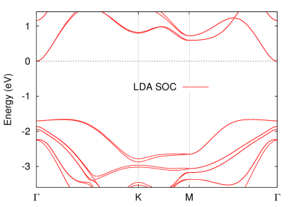
Fig. 4 shows the LDA band structure of the monolayer with spin-orbit coupling taken into account. The splitting is small, particularly so in the region of the -point, we therefore neglect it in the TB model. In the theory (see section VI), we include spin-orbit coupling to quantify how small it is near the -point, and to show how it is expected to behave at a larger number of layers.
IV Bilayer InSe: inter-layer hopping parameterized using DFT
We now extend the TB model to describe coupling between consecutive layers in -layer InSe. For this, we consider a bilayer and include hops in the -direction, XX, XM, and MX as depicted in Fig. 1d. The Hamiltonian can be written as
| (17) |
where and describe the individual monolayers comprising the bilayer structure, and describes the interaction between them and can be written as
| (18) |
where each term corresponds to a category of hopping interactions as labeled in Fig. 1d. The vertical M-X contribution is
| (19) | ||||
The creation and annihilation operators now have additional indices for layers and sublayers, e.g. annihilates (creates) an electron on layer (), atom X, in sublayer 2, in orbital . The sum over runs over all unit cells in the crystal. We denote inter-layer hopping parameters with a lowercase . For the other M-X inter-layer interaction we have
| (20) | ||||
while X-X hoppings are included in the form
| (21) | ||||
where the sums over are over nearest-neighboring X-X pairs and next-nearest-neighboring M-X pairs in adjacent sublayers. The inter-layer interactions included add 14 parameters to the model. When expressed in matrix form in a -space basis, the bilayer model gives a matrix, which we diagonalize to obtain a set of bands.
To obtain the parameters, we fit the TB band structure to the DFT band structure of bilayer InSe obtained within the local density approximation. In the DFT calculation the monolayer geometry was kept fixed and the inter-layer distance set to 8.32 Å, which corresponds to the experimentally known separation in -InSe Mudd et al. (2013). We search for the ideal set of inter-layer hopping parameters to achieve the best least squares fit between the two band structures while keeping the inter-layer hopping parameters obtained in the monolayer model unchanged. In the monolayer we fitted the model to DFT data for 7 bands near the Fermi level. In the bilayer these bands split into subbands forming 14 bands in total, all of which are taken into account in the fitting procedure. As in the monolayer, we fit to the scissor-corrected DFT data, since the dependence of the optical transition matrix elements on is significantly affected by the size of the band gap - this is explored in detail in appendix C.
The results of the fitting are presented alongside the DFT data for bilayer -InSe in Fig. 5, with the inter-layer TB parameters given in Table 4. We highlight the 8 bands derived from the monolayer bands , , , and ; we label these , , , , , , , and . The zero of energy is set at the bottom of the conduction band. We provide the orbital decomposition of the -point wave functions in Table 3.
| (eV) | 0.69 | 0.00 | -1.21 | -1.81 | -1.88 | -1.91 | -2.00 | -2.03 |
|---|---|---|---|---|---|---|---|---|
| (eV) | -2.20 | -2.80 | -2.87 | -2.90 | -2.99 | -3.02 | ||
| Se1 | 0.06[0.00] | 0.05[0.00] | 0.01[0.01] | 0.06[0.07] | 0.20[0.06] | 0.15[0.36] | 0.00[0.01] | 0.01[0.00] |
| 0.03[0.07] | 0.11[0.15] | 0.18[0.23] | 0.16[0.14] | |||||
| In1 | 0.10[0.05] | 0.12[0.11] | 0.03[0.07] | 0.01[0.00] | 0.04[0.01] | 0.03[0.00] | 0.00[0.03] | 0.00[0.00] |
| 0.06[0.05] | 0.00[0.07] | 0.06[0.01] | 0.07[0.02] | |||||
| In2 | 0.06[0.09] | 0.12[0.07] | 0.00[0.03] | 0.03[0.01] | 0.00[0.00] | 0.01[0.00] | 0.05[0.08] | 0.03[0.01] |
| 0.00[0.07] | 0.02[0.05] | 0.07[0.02] | 0.06[0.01] | |||||
| Se2 | 0.01[0.00] | 0.07[0.00] | 0.01[0.01] | 0.17[0.22] | 0.01[0.01] | 0.05[0.04] | 0.02[0.01] | 0.19[0.21] |
| 0.16[0.17] | 0.03[0.07] | 0.14[0.15] | 0.15[0.19] | |||||
| Se3 | 0.01[0.00] | 0.06[0.00] | 0.01[0.01] | 0.16[0.19] | 0.02[0.01] | 0.04[0.03] | 0.02[0.01] | 0.20[0.25] |
| 0.16[0.18] | 0.04[0.07] | 0.14[0.15] | 0.15[0.19] | |||||
| In3 | 0.06[0.07] | 0.11[0.08] | 0.00[0.02] | 0.03[0.00] | 0.00[0.00] | 0.01[0.00] | 0.05[0.10] | 0.04[0.01] |
| 0.01[0.03] | 0.02[0.07] | 0.08[0.02] | 0.06[0.01] | |||||
| In4 | 0.11[0.07] | 0.11[0.09] | 0.04[0.07] | 0.01[0.00] | 0.03[0.00] | 0.04[0.00] | 0.00[0.04] | 0.00[0.00] |
| 0.07[0.08] | 0.00[0.05] | 0.06[0.00] | 0.07[0.02] | |||||
| Se4 | 0.07[0.00] | 0.05[0.00] | 0.01[0.00] | 0.04[0.01] | 0.19[0.40] | 0.17[0.06] | 0.00[0.01] | 0.02[0.02] |
| 0.04[0.07] | 0.10[0.14] | 0.19[0.22] | 0.16[0.15] |
| -0.238 |
V TB model for few-layer InSe: 2D bands and gaps
Applying our TB model to few-layer InSe requires the generalization of the bilayer model as follows. As in the bilayer, we consider the interactions between the nearest-neighboring X-X pairs and nearest and next-nearest M-X pairs on adjacent monolayers. This gives us a Hamiltonian of the form
| (22) |
where is the total number of layers, is the monolayer Hamiltonian on layer as set out above, and takes into account inter-layer interactions between adjacent layers and . It has the form
| (23) |
The vertical M-X contribution is
| (24) | ||||
For the other M-X inter-layer interaction we have
| (25) | ||||
while X-X hoppings are included in the form
| (26) | ||||
where the sums over are over nearest-neighboring X-X pairs and next-nearest-neighboring M-X pairs in adjacent sublayers. When expressed in matrix form in a -space basis, the -layer model gives a matrix, which we diagonalize to obtain a set of bands. The matrix elements are given in the Appendix.
For the parameterization of the model we retain the hopping parameters from the bilayer model, corresponding to the approximation that the TB parameters will be the same for all values of . Fig. 6 shows the results of this extrapolation of the TB model to 3, 4, and 5.
The bottom right panel of Fig. 6 shows the vertical band gaps at according to the TB model at varying number of layers. If the band structure of bulk InSe is available along , one can extract the effective masses along the axis in the valence and conduction band, and respectively, and use these to apply the size-quantization gap model to approximate the expected gap for an -layer structure, . This approximation strictly speaking only works for , but can be easily extended to few-layer materials using the following asymptotic formula
| (27) |
with obtained from fitting to vertical gaps from the TB model. The parameter is present to allow the model to retain its validity at a small number of layers, in which case the traditional effective mass model would need to be used with a general boundary condition, , to take into account that the wave function is pushed to the surface of the few-layer slabs, as we see in the wave functions calculated using the TB model. The behavior described by Eq. (27) is shown by a solid line in the right-hand lower panel in Fig. 6.
VI 4-band theory for - layer InSe and interband optical transitions
In the following we present a simple model for the , , , and bands in Fig. 2. In monolayer InSe these bands can be assigned the irreducible representations of point group as seen in Fig. 2. The 4-band Hamiltonian can be written as
| (28) |
where the diagonal components are the single band Hamiltonians for the bands , , , and as discussed below, while the off-diagonal components correspond to the interaction between the electrons and photons required to describe optical transitions between the bands and , as well as between the bands and . The one-band description of the valence and conduction band is a straightforward polynomial expansion described below, while for bands and a suitable two-component Hamiltonian needs to be constructed that describes both branches in each band.
The bottom of the conduction band in 1L-InSe is quadratic in shape and can be described by the Hamiltonian
| (29) |
where is the electron wave-vector measured from the -point, is the effective mass at the conduction band minimum (listed in the caption of Fig. 7) and the second term in the Hamiltonian describes the spin-orbit splitting in the vicinity of the -point, and . The magnitude of the coupling constant is eVÅ3 as found by fitting the energy splitting between the two spin components in the conduction band up to wave vectors less than 0.06 1/Å. The spin-orbit splitting according to the local density approximation is presented in Fig. 4. The lack of a splitting along the line is in agreement with the trigonal symmetry exhibited by the second term in the Hamiltonian in Eq. (29). The last term in Eq. (29) appears in L-InSe only for and is present due to the breaking of the mirror-plane symmetry. The coefficient is expected to depend on the number of layers.
The highest valence bands in L-InSe are “sombrero-shaped” Zólyomi et al. (2014). The highest valence band can be fitted around the -point with an 8th order polynomial function as follows:
| (30) | ||||
where the coefficient describes the hexagonal anisotropy. The fitted parameters are summarized in Table 5. Note that the valence band takes the shape of an inverted sombrero which has been demonstrated to lead to a Lifshitz transition upon hole doping in the monolayer Zólyomi et al. (2014). The sombrero shape and the associated Lifshitz transition persists with increasing but slowly vanishes as we approach the bulk limit. Accordingly, the critical carrier density required to achieve the transition decreases with increasing , as shown in Table 5.
The last two terms in Eq. (30) describe the spin-orbit splitting similar to Eq. (29). The magnitude of according to a fit to the spin-orbit splitting in 1L-InSe for wave vectors less than 0.06 1/Å is eVÅ3. Note that the polynomial fit is valid in a 4-5 times larger range than the fit for the spin-orbit splitting.
| 1L | 2L | 3L | |
|---|---|---|---|
| (eV) | -0.078 | -0.069 | -0.056 |
| (eVÅ2) | 2.915 | 4.767 | 5.318 |
| (eVÅ4) | -38.057 | -106.817 | -163.540 |
| (eVÅ6) | 206.551 | 896.029 | 1894.272 |
| (eVÅ6) | 3.050 | 5.658 | 6.500 |
| (eVÅ8) | -450.034 | -2982.703 | -8844.573 |
| (cm-2) | 7.3 | 3.6 | 1.8 |
The bands and are double degenerate at the -point and can each be described by a two-component model as described by the Hamiltonian
| (31) |
where are the Pauli matrices. This Hamiltonian transforms according to the irrep. of the symmetry group (see Fig. 2). Eq. (31) can be fitted to the DFT band structure to obtain the effective masses. In the band we obtain and , and in the band we obtain and in units of .
In Fig. 7a we show the energies of the and optical transitions at the -point (energies and , respectively), where we apply the low-temperature scissor correction to the transition energies as discussed in Section III.2. On the right hand side we show the same data with scissor corrections for reference to room temperature measurements. The scissor corrected transition energies are summarized in the caption of Fig. 7.
| (eV) | (eV) | (eV) | () | (/Å) | (eÅ) | ||
|---|---|---|---|---|---|---|---|
| 1 | 1.602 / 1.933 | 2.734 / 3.066 | 2.584 / 2.916 | 0.188 | 0.000 | 1.096 | 1.68 |
| 2 | 1.031 / 1.695 | 2.164 / 2.827 | 2.014 / 2.677 | 0.148 | 0.082 | 1.055 | 2.87 |
| 3 | 0.796 / 1.601 | 1.929 / 2.734 | 1.779 / 2.584 | 0.132 | 0.132 | 1.119 | 3.72 |
To describe the coupling of the principal interband transition, A, between the conduction () and valence ( bands to an in-plane vector potential carried by an incoming photon, , we rely on the following formula for the interband momentum operator Lew Yan Voon and Ram-Mohan (1993):
| (32) | ||||
where the sum over runs over the orbitals in the model, is the coefficient of the eigenfunction of the conduction(valence) band, orbital , at , , and is the free electron mass. We can therefore calculate the interband momentum matrix element using the above TB parameterization, with the matrix elements of the Hamiltonian and the eigenfunctions of the valence and conduction bands obtained directly from the TB model.
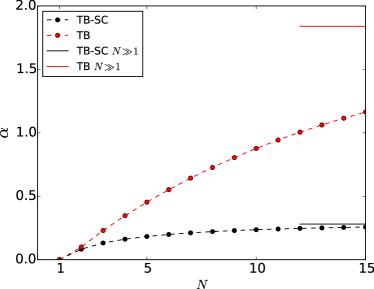
The TB matrix elements, seen in Fig. 7b, are linear at small and the slope of this linear regime increases with an increasing number of layers. The latter observation is in line with the result that the momentum matrix element in the monolayer is zero. The finding that the matrix element is linear near the -point allows the introduction of the dimensionless parameter through the relation which is taken into account in Eq. (28).
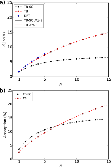
For coupling to the electric field associated with out-of-plane polarized light, we can also calculate the out-of-plane dipole matrix element between the valence and the conduction band. Since the crystal is finite in the direction we calculate the dipole matrix element directly as
| (33) |
where the sum over is over all orbitals in the unit cell, is the coefficient of the conduction (valence) band eigenfunction for orbital at , and is the -coordinate, w.r.t. the mean plane of the crystal, of the atom on which orbital sits.
The optical absorption coefficient for band edge absorption can be calculated from using Fermi’s golden rule. A perturbation of where is the electric field of the incoming photon, the rate of energy absorption in a material of dipole moment is
| (34) |
where is the photon energy, , and and are the band edge dispersions in the conduction and the valence band, respectively, as determined by theory. The absorption coefficient as a function of the angle between the incoming photon and the surface can be calculated simply by dividing by the absorbed energy, which is the flux of the Poynting vector over the visible area of the unit cell,
| (35) |
where is the unit cell area. Evaluating this expression yields for the absorption at
| (36) |
where is the conduction band effective mass.
For coupling of the transition between bands and , B, with in-plane polarized light, , we evaluate as
| (37) |
from which we find how the transition B absorbs in-plane polarized light, at ,
| (38) |
where has finite values at , listed in the caption to Fig. 7 for . In Fig. 7d we show the dependence of and on the number of layers ; while exhibits a strong dependence on , is almost constant.
VII Conclusions
We have developed a TB model to describe monolayer and few-layer indium selenide which takes into account all and orbitals of constituent atoms. We have used first principles density functional theory to parametrize the model. We have found that:
-
•
inclusion of and orbitals and hoppings to second-nearest-neighbors is sufficient to describe the energies of the bands near the band edge,
-
•
the interband optical matrix element obtained from our model exhibits a linear -dependence in agreement with DFT calculations, and
-
•
the matrix element vanishes in the monolayer due to symmetry.
We used the model to find the optical absorption coefficient in few-layer InSe: of the two principal optical transitions the absorption coefficient of the lower energy transition ( line), corresponding to band edge absorption between the conduction and the valence band, slowly increases with the number of layers, while the absorption for the higher energy transition ( line) saturates quickly to %.
Also, we find that the conduction band electrons are relatively light (), in contrast to an almost flat dispersion of valence band holes near the -point, which is found for up to . The latter property of the valence band suggests that this material may experience a phase transition due to many-body effects into either a ferromagnetic state as suggested for the similar material GaSe Cao et al. (2015), or into a Peierls-type charge density wave due to a strong electron-phonon coupling Zólyomi et al. .
The other members of the family of hexagonal III-VI semiconductors, such as GaSeZólyomi et al. (2013), have a similar crystal structure in the monolayer, and the TB model in section III could be extended to cover these materials. However, few-layer GaSe has a different consecutive layer arrangement, hence this will be covered in a future workMagorrian et al. .
Acknowledgements.
The authors thank A. Patanè, L. Eaves, A. V. Tyurnina, D. A. Bandurin, A. K. Geim, M. Potemski, and N. D. Drummond for discussions. This work made use of the facilities of N8 HPC provided and funded by the N8 consortium and EPSRC EP/K000225, the CSF cluster of the University of Manchester, and the High-End Computing cluster of Lancaster University. SJM acknowledges support from EPSRC CDT Graphene NOWNANO EP/L01548X. VF acknowledges support from ERC Synergy Grant Hetero2D, EPSRC EP/N010345, and Lloyd Register Foundation Nanotechnology grant. VZ and VF acknowledge support from the European Graphene Flagship Project.Appendix A Monolayer Hamiltonian matrix elements
A.1 Mirror plane symmetry
In a basis containing all and valence orbitals the Hamiltonian will be a matrix. We can reduce the system to two matrices by making use of the symmetry of the crystal structure, which will require that the wavefunction be even or odd w.r.t. exchange of the two sublayers. We therefore construct a new basis from even and odd combinations of our orbitals:
| (39) | ||||
where and orbitals have an extra sign on the bottom sublayer contribution as the direction of is reversed under . A matrix constructed in the above basis will be block-diagonal, as mixing between even and odd states would break symmetry.
A.2 Representation
To calculate our Hamiltonian we express it in a -space basis, constructing a matrix with elements where and are the annihilation (creation) operators for the orbitals in our basis at wave vector in the Brillouin zone. The operators can be expressed with the real space annihilation (creation) operators as
| (40) |
where is the position of the real space orbital , and is the number of lattice sites.
Relying on the symmetry adapted basis, we represent our Hamiltonian as two matrices in the -space basis with elements of the form:
| (41) | ||||
Now substituting in the original forms of the even and odd basis, we get for two orbitals where neither are
| (42) | ||||
As the system and the Hamiltonian are even under we can observe that
| (43) | ||||
and hence
| (44) | ||||
In the case where orbital is we have
| (45) | ||||
We therefore need only consider , and in the calculation of our Hamiltonian matrix. We can then diagonalize the even and odd parts of the Hamiltonian separately, obtaining a set of 8 bands for each. The matrices have the form
| (46) |
The elements are calculated as set out above. For the calculation of the Bloch phase factors we can reduce the hopping vectors to three sets, as the Brillouin zone is two-dimensional. These are for M-X hoppings
| (47) |
and for M-M and X-X hoppings between ions in the same sublayer ( for M-M hopping between the two sublayers, where the ions are directly above each other) there are six such vectors
| (48) |
For next-nearest M-X pairs () we have
| (49) |
The -dependence then appears in the model through combinations of the Bloch phase factors calculated using these vectors
| (50) | ||||
The symbols and are the magnitudes of the hopping vectors for M-X intra- and inter-sublayer hoppings, respectively, and are given by
| (51) | ||||
The matrix elements are:
A.2.1 Diagonal elements
A.2.2 M-X Off-diagonal elements
A.2.3 M-M, X-X off-diagonal elements
Appendix B Inter-layer Hamiltonian matrix elements
The Hamiltonian for bilayer -InSe is expressed in the form
| (52) |
where is the monolayer Hamiltonian, expressed in the original atomic basis (, , , , as opposed to the even/odd basis used above), and includes the inter-layer interactions. We write as
| (53) |
where represents the vertical M-X interactions, and has the form
| (54) |
The elements themselves are
| (55) | ||||
| (56) | ||||
| (57) | ||||
| (58) | ||||
| (59) |
represents the X-X interactions, with
| (60) |
In the expressions for the elements, is the length of the inter-layer X-X hop, and is given by
| (61) |
The elements are
| (62) | ||||
In the case of the non-vertical M-X hops we have
| (63) |
with matrix elements
| (64) | ||||
where the length of the hop is given by
| (65) |
For greater numbers of layers we build up the matrix such that is on the diagonal blocks, with adjacent diagonal blocks connected by and .
Appendix C Comparison between scissor corrected TB, uncorrected TB, and DFT optical matrix elements
For comparison, we also obtain the matrix elements from density functional theory and from a TB model without scissor-correction. In a DFT calculation utilizing a plane-wave basis, the momentum matrix element is straightforward to calculate as
| (66) |
where and are the plane-wave coefficients and the reciprocal lattice vectors taken into account in the plane-wave basis set, respectively. is calculated in DFT by real space integration on a sufficiently fine grid. The intralayer TB parameters for the uncorrected model are given in Table 1 in the main text, while the interlayer parameters are given in Table 6.
| -0.332 |
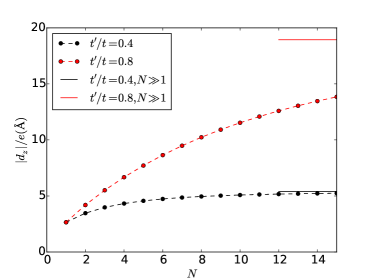
In the main text we apply a scissor correction to the DFT band structure in order to account for the underestimation of the band gap. It should be noted that the scissor correction is necessary for another reason as well. The TB model, when fitted to DFT band structures without scissor correction, agrees well with the DFT results for at small (see Fig. 10a). However, the extrapolation to large is considerably larger, and the saturation much slower, than that for the TB model calculated with scissor correction. Likewise, the coefficient of the linear regime (Fig. 9) is also larger if the scissor correction is omitted. In essence, uncorrected DFT overestimates matrix elements, whereas the scissor correction leads to a significant reduction in , and in turn a reduced absorption.
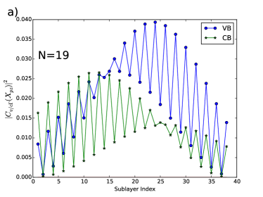
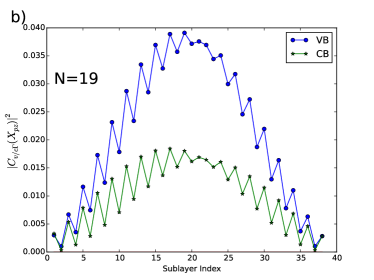
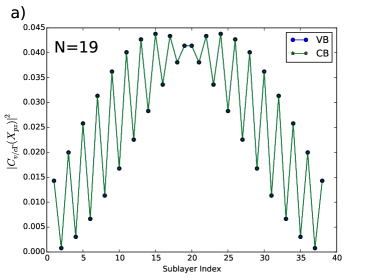
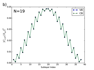
The origin of the reduction in when applying the scissor correction lies in the effect the scissor correction has on the TB wave functions for . Fig. 11a shows the modulus square of the chalcogen TB wave function coefficients as a function of the sublayer index in 19-layer InSe. The wave function reduces towards the edge of the slab but a clear finite value remains at the very edge, due to a substantial oscillation in the coefficients, which gives a substantial contribution to . Fig. 11b shows the same wave function coefficients after scissor correction. Note that the relative weight of the coefficient at the edge has now decreased, as has the aforementioned oscillation, which leads to an overall smaller and a faster saturation with increasing .
The physics behind the reduction of the wave function at the edge is the relative reduction of the inter-layer interaction as compared to the intra-layer interaction, which is a direct consequence of the scissor correction. By increasing the gap without changing the band width caused by inter-layer hopping, the intra-layer hopping becomes stronger while the inter-layer hopping remains at the same magnitude. This can be understood within a chain model, which we discuss below.
The core message here is that the scissor correction has an effect on the wave functions and in turn on the optical properties of InSe slabs, and should be taken into account when modeling few-layer InSe.
Appendix D Chain model for few-layer InSe at
The simplest way to describe a layered semiconductor is by approximating each layer with a dimer, each atom hosting a single basis orbital and . In this case, the monolayer can be described by a single hopping integral and the Hamiltonian will be
| (67) |
where annihilates (creates) an electron on sublayer 2, site . Expressed in matrix form the Hamiltonian is
| (68) |
The Hamiltonian of a few-layer structure is
| (69) | ||||
where is the layer index, and the inter-layer interaction is described by the hop . As an example, the matrix form of a bilayer can be written as
| (70) |
which has the following eigenvalues:
| (71) | ||||
In this chain model, the ratio characterizes the strength of the inter-layer interaction with respect to the intra-layer coupling. Let us now assume that we can describe few-layer InSe with such a model, with some values for the two hopping parameters obtained from DFT calculations. When we implement a scissor correction, we leave the inter-layer hop unchanged while we increase the magnitude of since, in the monolayer, the band gap from this model is simply . Hence, a scissor correction translates to a decrease in the ratio .
This finding allows us to demonstrate the qualitative effect of the scissor correction. Fig. 12 shows the modulus square of the coefficients of the chain model wave functions in the valence and conduction band. Panel a) corresponds to , while panel b) to . The visible reduction of the wave function along the edges upon decreasing is in agreement with the effects of the scissor correction on the full model (see Fig. 11). Similarly, if we now plot the matrix element from the chain model (Fig. 13) we find that the matrix element undergoes significant reduction when we decrease , just like it happened in the full model when we implemented the scissor correction there (see Fig. 10a).
References
- Bandurin et al. (2016) D. Bandurin, A. Tyurnina, G. Yu, A. Mishchenko, V. Zólyomi, S. Morozov, R. K. Kumar, R. Gorbachev, Z. Kudrynskyi, S. Pezzini, Z. D. Kovalyuk, U. Zeitler, K. S. Novoselov, A. Patane, L. Eaves, I. V. Grigorieva, V. I. Fal’ko, A. K. Geim, and Y. Cao, Nature Nanotechnology, doi:10.1038/nnano.2016.242 (2016).
- Yoffe (1973) A. D. Yoffe, Ann. Rev. Matt. Sci. 3, 147 (1973).
- Novoselov et al. (2005) K. S. Novoselov, D. Jiang, F. Schedin, T. J. Booth, V. V. Khotkevich, S. V. Morozov, and A. K. Geim, Proceedings of the National Academy of Sciences of the United States of America 102, 10451 (2005).
- Gorbachev et al. (2011) R. V. Gorbachev, I. Riaz, R. R. Nair, R. Jalil, L. Britnell, B. D. Belle, E. W. Hill, K. S. Novoselov, K. Watanabe, T. Taniguchi, A. K. Geim, and P. Blake, Small 7, 465 (2011).
- Mak et al. (2010) K. F. Mak, C. Lee, J. Hone, J. Shan, and T. F. Heinz, Physical Review Letters 105, 136805 (2010).
- Splendiani et al. (2010) A. Splendiani, L. Sun, Y. Zhang, T. Li, J. Kim, C.-Y. Chim, G. Galli, and F. Wang, Nano letters 10, 1271 (2010).
- Korn et al. (2011) T. Korn, S. Heydrich, M. Hirmer, J. Schmutzler, and C. Schüller, Applied Physics Letters 99, 102109 (2011).
- Wang et al. (2012) Q. H. Wang, K. Kalantar-Zadeh, A. Kis, J. N. Coleman, and M. S. Strano, Nature Nanotechnology 7, 699 (2012).
- Xu et al. (2014) X. Xu, W. Yao, D. Xiao, and T. F. Heinz, Nature Physics 10, 343 (2014).
- Jones et al. (2013) A. M. Jones, H. Yu, N. J. Ghimire, S. Wu, G. Aivazian, J. S. Ross, B. Zhao, J. Yan, D. G. Mandrus, D. Xiao, W. Yao, and X. Xu, Nature nanotechnology 8, 634 (2013).
- Gan et al. (2013) X. Gan, Y. Gao, K. F. Mak, X. Yao, R.-J. Shiue, A. van der Zande, M. E. Trusheim, F. Hatami, T. F. Heinz, J. Hone, and D. Englund, Applied physics letters 103, 181119 (2013).
- Wu et al. (2014) S. Wu, S. Buckley, A. M. Jones, J. S. Ross, N. J. Ghimire, J. Yan, D. G. Mandrus, W. Yao, F. Hatami, J. Vučković, A. Majumdar, and X. Xu, 2D Materials 1, 011001 (2014).
- Sie et al. (2015) E. J. Sie, J. W. McIver, Y.-H. Lee, L. Fu, J. Kong, and N. Gedik, Nature materials 14, 290 (2015).
- Wang et al. (2015) G. Wang, X. Marie, I. Gerber, T. Amand, D. Lagarde, L. Bouet, M. Vidal, A. Balocchi, and B. Urbaszek, Physical review letters 114, 097403 (2015).
- Liu et al. (2015) X. Liu, T. Galfsky, Z. Sun, F. Xia, E.-c. Lin, Y.-H. Lee, S. Kéna-Cohen, and V. M. Menon, Nature Photonics 9, 30 (2015).
- Lei et al. (2014) S. Lei, L. Ge, S. Najmaei, A. George, R. Kappera, J. Lou, M. Chhowalla, H. Yamaguchi, G. Gupta, R. Vajtai, A. D. Mohite, and P. M. Ajayan, ACS Nano 8, 1263 (2014).
- Mudd et al. (2013) G. W. Mudd, S. A. Svatek, T. Ren, A. Patanè, O. Makarovsky, L. Eaves, P. H. Beton, Z. D. Kovalyuk, G. V. Lashkarev, Z. R. Kudrynskyi, and A. I. Dmitriev, Advanced Materials 25, 5714 (2013).
- Mudd et al. (2014) G. W. Mudd, A. Patanè, Z. R. Kudrynskyi, M. W. Fay, O. Makarovsky, L. Eaves, Z. D. Kovalyuk, V. Zólyomi, and V. Falko, Applied Physics Letters 105, 221909 (2014).
- Mudd et al. (2015) G. W. Mudd, S. A. Svatek, L. Hague, O. Makarovsky, Z. R. Kudrynskyi, C. J. Mellor, P. H. Beton, L. Eaves, K. S. Novoselov, Z. D. Kovalyuk, E. E. Vdovin, A. J. Marsden, N. R. Wilson, and A. Patanè, Advanced Materials 27, 3760 (2015).
- Tamalampudi et al. (2014) S. R. Tamalampudi, Y.-Y. Lu, R. Kumar U, R. Sankar, C.-D. Liao, K. Moorthy B, C.-H. Cheng, F. C. Chou, and Y.-T. Chen, Nano Letters 14, 2800 (2014).
- Balakrishnan et al. (2014) N. Balakrishnan, Z. R. Kudrynskyi, M. W. Fay, G. W. Mudd, S. A. Svatek, O. Makarovsky, Z. D. Kovalyuk, L. Eaves, P. H. Beton, and A. Patanè, Advanced Optical Materials 2, 1064 (2014).
- Damon and Redington (1954) R. W. Damon and R. W. Redington, Physical Review 96, 1498 (1954).
- Likforman et al. (1975) A. Likforman, D. Carre, J. Etienne, and B. Bachet, Acta Crystallographica Section B: Structural Crystallography and Crystal Chemistry 31, 1252 (1975).
- Williams et al. (1977) R. Williams, J. McCanny, R. Murray, L. Ley, and P. Kemeny, Journal of Physics C: Solid State Physics 10, 1223 (1977).
- Manjón et al. (2004) F. J. Manjón, A. Segura, V. Muñoz-Sanjosé, G. Tobías, P. Ordejón, and E. Canadell, Physical Review B 70, 125201 (2004).
- Manjón et al. (2001) F. J. Manjón, D. Errandonea, A. Segura, V. Muñoz, G. Tobías, P. Ordejón, and E. Canadell, Physical Review B 63, 125330 (2001).
- Pellicer-Porres et al. (1999) J. Pellicer-Porres, A. Segura, V. Muñoz, and A. San Miguel, Physical Review B 60, 3757 (1999).
- Goi et al. (1992) A. R. Goni, A. Cantarero, U. Schwarz, K. Syassen, and A. Chevy, Physical Review B 45, 4221 (1992).
- Kress-Rogers et al. (1982) E. Kress-Rogers, R. Nicholas, J. Portal, and A. Chevy, Solid State Communications 44, 379 (1982).
- Gorshunov et al. (1998) B. Gorshunov, A. Volkov, A. Prokhorov, M. Kondrin, A. Semeno, S. Demishev, A. Dmitriev, Z. Kovalyuk, and G. Lashkarev, Solid State Communications 105, 433 (1998).
- Dmitriev et al. (1995) A. Dmitriev, G. Lashkarev, V. Kiselyev, V. Kononenko, and E. Kuleshov, International journal of infrared and millimeter waves 16, 775 (1995).
- Millot et al. (2010) M. Millot, J. M. Broto, S. George, J. González, and A. Segura, Phys. Rev. B 81, 205211 (2010).
- Segura et al. (1983) A. Segura, J. Guesdon, J. Besson, and A. Chevy, Journal of applied physics 54, 876 (1983).
- Segura et al. (1997) A. Segura, J. Bouvier, M. V. Andrés, F. J. Manjón, and V. Muñoz, Physical Review B 56, 4075 (1997).
- McCanny and Murray (1977) J. V. McCanny and R. B. Murray, Journal of Physics C: Solid State Physics 10, 1211 (1977).
- De Blasi et al. (1983) C. De Blasi, G. Micocci, A. Rizzo, and A. Tepore, Physical Review B 27, 2429 (1983).
- Camassel et al. (1978a) J. Camassel, P. Merle, H. Mathieu, and A. Chevy, Physical Review B 17, 4718 (1978a).
- (38) G. W. Mudd, M. R. Molas, X. Chen, V. Zólyomi, K. Nogajewski, Z. R. Kudrynskyi, Z. D. Kovalyuk, G. Yusa, O. Makarovsky, L. Eaves, M. Potemski, V. I. Fal’ko, and A. Patanè, Accepted for publication in Scientific Reports.
- Zólyomi et al. (2014) V. Zólyomi, N. D. Drummond, and V. I. Fal’ko, Physical Review B 89, 205416 (2014).
- Rybkovskiy et al. (2014) D. V. Rybkovskiy, A. V. Osadchy, and E. D. Obraztsova, Physical Review B 90, 235302 (2014).
- Sun et al. (2016) C. Sun, H. Xiang, B. Xu, Y. Xia, J. Yin, and Z. Liu, Appl. Phys. Express 9, 035203 (2016).
- Slater and Koster (1954) J. C. Slater and G. F. Koster, Physical Review 94, 1498 (1954).
- Kresse and Furthmüller (1996) G. Kresse and J. Furthmüller, Physical Review B 54, 11169 (1996).
- Fiorentini and Baldereschi (1995) V. Fiorentini and A. Baldereschi, Phys. Rev. B 51, 17196 (1995).
- Johnson and Ashcroft (1998) K. A. Johnson and N. W. Ashcroft, Phys. Rev. B 58, 15548 (1998).
- Bernstein et al. (2002) N. Bernstein, M. J. Mehl, and D. A. Papaconstantopoulos, Phys. Rev. B 66, 075212 (2002).
- Parashari et al. (2008) S. S. Parashari, S. Kumar, and S. Auluck, Physica B 403, 3077 (2008).
- Thilagam et al. (2010) A. Thilagam, D. J. Simpson, and A. R. Gerson, J. Phys. Cond. Matt. 23, 025901 (2010).
- Babu et al. (2011) K. R. Babu, C. B. Lingam, S. Auluck, S. P. Tewari, and G. Vaitheeswaran, J. Sol. State Chem 184, 343 (2011).
- Camassel et al. (1978b) J. Camassel, P. Merle, H. Mathieu, and A. Chevy, Phys. Rev. B 17, 4718 (1978b).
- Lew Yan Voon and Ram-Mohan (1993) L. C. Lew Yan Voon and L. R. Ram-Mohan, Physical Review B 47, 15500 (1993).
- Cao et al. (2015) T. Cao, Z. Li, and S. G. Louie, Physical Review Letters 114, 236602 (2015).
- (53) V. Zólyomi, S. J. Magorrian, M. Calandra, F. Mauri, and V. I. Fal’ko, Unpublished.
- Zólyomi et al. (2013) V. Zólyomi, N. D. Drummond, and V. I. Fal’ko, Physical Review B 87, 195403 (2013).
- (55) S. J. Magorrian, V. Zólyomi, and V. I. Fal’ko, Unpublished.