Signature of Hanle Precession in Trilayer MoS2: Theory and Experiment
Abstract
Valley-spin coupling in transition-metal dichalcogenides (TMDs) can result in unusual spin transport behaviors under an external magnetic field. Nonlocal resistance measured from 2D materials such as TMDs via electrical Hanle experiments are predicted to exhibit nontrivial features, compared with results from conventional materials due to the presence of intervalley scattering as well as a strong internal spin-orbit field. Here, for the first time, we report the all-electrical injection and non-local detection of spin polarized carriers in trilayer MoS2 films. We calculate the Hanle curves theoretically when the separation between spin injector and detector is much larger than spin diffusion length, . The experimentally observed curve matches the theoretically-predicted Hanle shape under the regime of slow intervalley scattering. The estimated spin life-time was found to be around at K.
pacs:
72.25.Dc, 75.40.Gb, 73.50.-h, 85.75.-d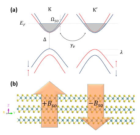
I Introduction
The discovery of two-dimensional (2D) transition metal dichalcogenides (TMDs) has attracted considerable attention recently due to their exotic properties, which are very important for their applications in electronic, optoelectronic, and spintronic devices [1, ; 2, ; 3, ; 4, ]. Some members of the TMD family possess spin as well as valley degrees of freedom which make them attractive for next-generation quantum computing applications too. One of the most studied examples of above materials is MoS2, which, contrary to graphene, possesses a band gap of eV in its monolayer form [5, ]. The valleys in 2D MoS2 are located at two energetically equivalent symmetry points, and , in the hexagonal Brillouin zone. Unlike graphene, the electron states in and valleys are not equivalent. Because of large spin orbit coupling (SOC) which originates from the d orbitals of heavy Mo atoms [8++, ; 9, ; 10, ; 11, ] and the inversion asymmetry induced Dresselhaus coupling [7, ; 12, ; 13, ; 14, ], the valence band edges of 2D MoS2 undergo a large spin splitting (150 meV). Furthermore, the Hamiltonian of 2D MoS2 possesses time reversal symmetry, which leads the two valleys to exhibit opposite sign of spin-orbit field, see Fig.1 [6, ; 7, ; 8, ]. Because of the above unique characteristics, the spin and valley degrees of freedom in 2D MoS2 can be controlled and manipulated independently, leading to its potential for applications in next-generation valleytronics-based devices.
Despite MoS2’s great potential in future spintronic devices, there are still very few experimental studies on the spin transport and relaxation mechanisms operating in the material [14+1, ; 14+2, ; 14+3, ]. Among those, the most noteworthy study is by Yang et al. [15, ] in which they used optical Hanle-Kerr experiment to measure the coupled spin-valley dynamics in 2D MoS2 and observed a long spin lifetime of at 5 K. Though the above observation is very important for obtaining fundamental understanding of the spin-valley dynamics, it is also important to explore spin transport characteristics of the material using all-electrical techniques. Nonlocal Hanle techniques have been widely used to investigate spin transport in several semiconducting systems, see e.g. Refs. [16, ; 19, ; Ian, ; 17, ; 18, ; 22, ; 29, ], however, there are no such reports for 2D MoS2.
In nonlocal Hanle measurements, spin polarized carriers are injected into the semiconductor channel from a magnetized ferromagnetic electrode. Accumulated spin-polarization just below the injector electrode diffuses in the channel and creates spin imbalance below the detector electrode. This imbalance results in a voltage signal in the detector. However, when a transverse magnetic field is applied, the spin of the electrons starts precessing around the applied field and the voltage falls off. The decay of voltage with magnetic field is referred to as Hanle curve. Its shape yields important information about the spin lifetime and spin diffusion length [silsbee1, ; silsbee2, ].
One reason which is probably responsible for the lack of reports on nonlocal Hanle studies on 2D MoS2 is that large area films were not availabe until recently. Nonlocal Hanle experiments require four electrode contacts and at least two of those contacts must be long enough so that their shape anisotropy preserve their in-plane magnetization when a traverse magnetic field is applied. These experimental requirements are indeed quite challenging in the case of micron sized MoS2 films normally produced by exfoliation based techniques. However, recently the growth of centimeter-scale high-quality 2D MoS2 films by CVD and PVD techniques has been demonstrated by several groups [3, ; 26, ; CVD, ]. Availability of these relatively large area films now can catalyze the spin transport studies on this exotic material system.
Other important factor, which possibly precluded the Hanle studies is the fact that 2D MoS2 possesses very strong out-of-plane intrinsic magnetic fields. These built-in fields, which originate due to the lack of inversion symmetry in the monolayer MoS2, can be of the order of several Tesla [32, ]. Since in electrical Hanle experiments the spin of the injected electrons is oriented in the plane of the channel, the intrinsic fields that are in the transverse direction can cause immediate precession and dephasing. In our previous theoretical study, we showed that the Hanle curve under normal field orientation exhibits a two-peak structure with maxima located at the values of external field , where is internal spin-orbit field. For monolayer MoS2 the value of is in the range of a few Tesla [32, ]. Thus, in experiments where the measurements are performed over a small out-of-plane external field interval, the peaks cannot be detected.
While the strength of SOC in monolayer MoS2 is expected to be the strongest, it is expected that SOC will also be present in other inversion asymmetric odd-layered MoS2 films, see Ref. [13, ]. The magnitude of SOC is supposed to decrease on increasing the number of layers. As a result, the two peaks will get progressively closer and might fall within the measurement range.
With this motivation, we performed nonlocal Hanle measurements on trilayer MoS2 films and obtained nontrivial results, which we report in this paper. To compare these results with theory, we have also extended our previous theoretical work Ref. [25, ] to incorporate the case of a finite distance between injector and detector.
The paper is organized as follows. In Section II, we discuss the sample preparation, characterization and Hanle experiments. Section III describes a theoretical model used in our study. In Section IV, we present our experimental Hanle results and compare them with theory.
II EXPERIMENTAL DETAILS
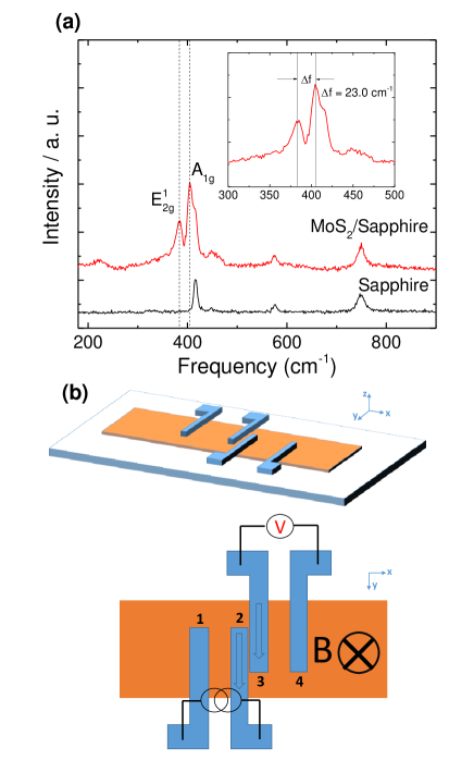
Trilayer MoS2 films were grown on sapphire substrates by pulsed laser deposition (PLD) following the procedure described in previous report [26, ]. The number of monolayers deposited was controlled precisely by controlling the number of laser pulses. After deposition, Raman spectra were collected from the MoS2 films as shown in Fig. 2(a). The two Raman vibrational modes, and , confirm the presence of MoS2. In prior studies it has been demonstrated that the separation between these modes can be used to determine the number of monolayers [3, ]. The observed peak separation of in the present study confirmed the formation of trilayer Mo.
Electrical Hanle measurements were conducted using a four probe geometry as shown in Fig. 2(b). The pattern of ferromagnetic (FM) contacts was fabricated through photolithography, and electron beam evaporation was used to deposit nm thick NiFe contacts. After lift-off, the edge-to-edge separation of the middle two contacts was found to be 1 .
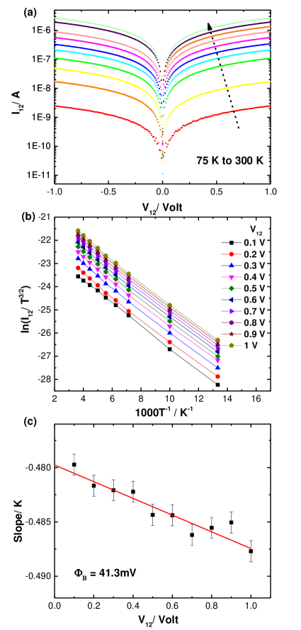
I-V measurements performed between contact 1 and 2 showed the presence of a Schottky barrier between NiFe and MoS2. Presence of this barrier elinimated the need for depositing any additional tunnel barrier layer[24, ; 27, ]. To determine the Schottky barrier height (), temperature dependent I-V curves were recorded. Fig.3(a) shows the I-V curves at different temperatures on a logarithmic scale. The barrier height was extracted using the thermionic emission function described in Appendix A. For this, first of all, vs. was plotted for various values as shown in Fig. 3(b). In the next step, slopes of these plots were determined as a function of (see Fig. 3(c)). From the y-axis intercept of Slope vs. plot, value of Schottky barrier height was determined to be mV. For Hanle measurement, the current was passed between first two contacts, 1 and 2, while the non-local voltage, , is measured through the other two contacts, 3 and 4.
III THEORY
In the theory of the Hanle effect [silsbee1, ; silsbee2, ; 28, ; 21, ; roundy, ], the nonlocal resistance, , is related to the spin density, , as follows
| (1) |
where is the Larmor frequency, = , is the spin injection/detection polarization, D is the diffusion coefficient related to the mobility () via the Einstein relation, , is the resistivity of channel material, is the cross-sectional area of the channel, and is the diffusion propagator defined as:
| (2) |
In above equation, denotes the distance between the injector and detector electrodes.
The shape of the Hanle curve depends on the relation between and the spin diffusion length, . In Ref. [25, ] we considered the case . With regard to our present experimental study, the opposite limit is relevant. Physically, in this limit, the Hanle curve is expected to exhibit numerous oscillations due to the fact that the spin of injected electron can accomplish integer number of full precessions before it reaches the detector [21, ].
The unique characteristics of the spin dynamics in
TMDs originates from the fact that there exist two groups of
spins corresponding to two valleys and . Due to a finite intervalley scattering rate, , the time evolution of and is described by the following system of coupled equations:
| (3) |
where . The above equations reflect the fact that the external field, , adds to the internal spin-orbit field in the valley and in the valley , see Fig. 1.
The system Eq. (III) should be solved with initial conditions, , which reflects the fact that at the moment of injection the spin is directed along the -axis. In our earlier paper Ref. [25, ] we have demonstrated that the analytical solution of the system depends on the dimensionless ratio
| (4) |
For a slow intervalley scattering, , the solution for the projection of the net spin, , reads
| (5) |
where we have introduced modified spin-orbit coupling
| (6) |
From Eq. (III) the calculation of nonlocal resistance is straightforward and the result can be obtained in a closed form. This is apparent, because, in the absence of spin-orbit coupling, the integral of the product appears in the expression for the conventional Hanle shape and can be evaluated analytically. In our case, is the combination of two oscillating functions. Final result for reads
| (7) |
is the prefactor which depends on spin injection/detection polarization, channel dimensions, and material resistivity [R_0, ]. Parameters and entering into Eq. (III) are defined as:
| (8) |
where is the dimensionless distance
| (9) |
and is the inverse spin relaxation rate. In the absence of other relaxation mechanisms, this rate is determined by the intervalley scattering rate. In the presence of additional mechanisms, this rate is the sum of the partial rates
| (10) |
III.1 The case of slow intervalley scattering
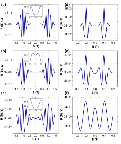
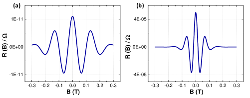
In Fig. 4 the Hanle curves plotted using Eq. (III) for two different values of spin-orbit field and several sets of are shown. For these plots, the value of parameter was chosen to be . As can be seen, the nonlocal resistance decays away from in an oscillatory fashion. Naturally, for shorter , the decay of oscillations is faster. For “strong” T (as in a monolayer) the most pronounced oscillations take place away from the origin. However, with regard to experiment, we are interested in the behavior of nonlocal resistance only within the domain T. For this reason, the central regions of the plots are enlarged. We see that the evolution of the Hanle shape near is quite lively, so that the shape changes significantly even when changes slightly from ps and ps. Still, the distance between the two maxima exceeds T for all near . For a smaller value of the spin-orbit field, T the behavior of nonlocal resistance near evolves with increasing as follows. There are pronounced oscillations at ps, less pronounced at ps, and almost no oscillations for ps. This behavior is the consequence of the fact that the bigger is , the more “bound” are the oscillations to the points T. Still, in all three curves the distance between the left and right extrema is close to T near .
III.2 The case of fast intervalley scattering
For fast intervalley scattering we have and the expression Eq. (III) for spin dynamics does not apply anymore. Physically, in the domain of fast intervalley scattering spin-orbit field effectively averages out as a result of fast switching of a carrier between the valleys. The modes of spin dynamics in the domain are classified into valley-symmetric (we denote it with ) and valley-asymmetric (). As a result of averaging out of the mode has a long lifetime, , while the lifetime of the symmetric mode is . The actual form of in the domain is still the sum of the products of oscillating and exponentially decaying functions, as we have demonstrated in Ref. [25, ]. This allows to calculate the Hanle curve explicitly for finite separation, , between the contacts. The result, representing the sum of contributions from and modes, reads
| (11) |
The notations in Eq. (III.2) are the following
| (12) |
The relaxation times in Eq. (III.2) are defined as
| (13) |
Two values of result in two spin diffusion lengths, , so that in Eq. (III.2) is equal to and is equal to .
Fig. 5 shows the resulting Hanle curves calculated from Eq. (III.2) for different values of . A distinctive feature of these curves compared to Fig. 4 is that falls off from with oscillations, so that the maximum at is the highest.
IV EXPERIMENTAL HANLE DATA
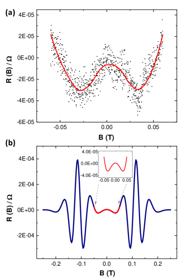
Fig. 6 shows the experimental Hanle data recorded at . Measurements of nonlocal resistance were performed using the experimental geometry shown in Fig. 2(b). Before measurements, injector and detector contacts were magnetized parallel to each other by applying an in-plane magnetic field which was parallel to the length of the electrode. Once the electrodes were magnetized, in-plane field was removed and a perpendicular magnetic field was applied to record Hanle data. To avoid the misalignment of the injector and detector magnetization, the out-of plane magnetic field was restricted between mT. For Hanle measurements, current was applied between electrode 1 and 2, and the voltage was measured between 3 and 4 while the transverse magnetic field was scanned from mT to mT.
Some salient features of the observed vs. curve are: (a) value of at T is almost zero; (b) on increasing the magnetic field, the sign of becomes negative and its magnitude starts increasing on either side of T; (c) at around T, the magnitude of starts decreasing and finally at T, again becomes zero; (d) after T, become positive and its magnitude increases with increase in field. The above features are obviously very different from the typical Hanle curves shown by normal materials where a maxima is observed at T in vs. curve. In order to understand the mechanism responsible for the observed behavior, we compare the experimental data with our theoretical prediction discussed in section III.
First of all, a quick comparison of the curve shown in Fig. 6(a) with theoretical curves shown in Fig. 4 and Fig. 5, suggested that the sample under investigation is in the regime . Specifically if the sample was in the regime , it should have exhibited a maxima at T in vs. curve. Once we found out the regime to which our sample belongs, we fitted the experimental data to the corresponding expression, i.e. equation (III). In equation (III), there are four independent unknown parameters namely, , , , and , all of which were varied during the fitting procedure. Figure of merit of the fit was determined by calculating the quantity .
The experimental data was found to fit very well in equation (7) with a value of . Fitted curve is shown by solid red curve in Fig. 6(a). The best fitting parameters were found to be T, , , and .
It is important to note that even though, because of experimental constraints, range over which we could scan the out-of-plane field was limited to mT, we could estimate which was much higher than that field. Now using the experimental determined values of , , , and , in equation (III), we calculated the curve over a magnetic field range of T and obtained a curve shown in Fig. 6(b).
The curve exhibits two peak structure with maxima located at T corresponding to two valleys. Furthermore, both of the peaks are accompanied with oscillatory signal on both sides of the main peaks which is understood to arise because of the integer number of full precession accomplished by the spin of the injection electrode before it reaches the detector electrode.
It is interesting to note that though the main Hanle peaks belonging to two valleys are well separated corresponding oscillatory peaks overlap near the origin and give rise to the shape in vs. plot as observed in our experiment. See the part of curve shown in red line in Fig. 6(b).
To check the consistency of the fit, from the values of and obtained above by the fitting of experimental data, we calculate the intervalley scattering rate . If the mobility is limited entirely by the intervalley scattering, it is related to and the carrier density as [25, ]
| (14) |
Using the value of mobility obtained from the fit, and the value of density from Ref. [3] we got the value in reasonable agreement with inferred from the fit.
V CONCLUDING REMARKS
(i) In summary, using the all-electrical technique of injecting and detecting spin polarized carriers, we have observed the signature of Hanle precession in trilayer MoS2 films.
(ii) Our theoretical calculations showed that because of the valley-specific spin-orbit field present in the odd-layered MoS2 films, two distinct Hanle peaks centered at are expected.
(iii) In the case of trilayer MoS2, the strength of field is much smaller than that for monolayer films. As a result, under certain experimental conditions, secondary oscillatory signals belonging to the two valleys can overlap and give rise to a detectable signal near the zero external magnetic field.
(iv) By comparing the experimental data with the theoretically predicted results, we found that the trilayer MoS2 films prepared by PLD undergo a slow intervalley scattering which is very important from the point of view of realizing practical valleytronic devices. A spin life-time of around was estimated at K.
(v) Here, it is also very instructive to compare the results of our all-electrical study with the study reported in [Crooker, ] where the optical techniques were employed for spin injection and detection in monolayer MoS2. To achieve the optical response the authors had to apply the normal magnetic field as high as T. In the present study, we observed the sensitivity of the spin transport in trilayer MoS2 to much smaller fields. One reason for this observed difference is the fact that in trilayer MoS2, field is much smaller than that in monolayer MoS2. The other reason, more important from the point of view of spin-transport, is that in our present transport measurement geometry, the injector and detector were separated by distance much longer than the spin diffusion length. As a result, the nonlocal voltage is created not by typical electrons, which loose their spin memory after time , but by electrons that escape relaxation for a long time before reaching the detector. Precession of these electrons is substantial in much weaker fields. As a result, the Hanle signal is weak, but still distinguishable.
(vi) Availability of large-area trilayer MoS2 films, in which valley specific spin transport can be investigated by electrical means, is likely to expedite further research in this area.
VI ACKNOWLEDGEMENTS
This work was supported by NSF through grant No. 1407650 and 1121252.
Appendix A Calculation of Schottky barrier height using thermionic equation
In the case of 2D materials, the thermionic emission equation is [27, ]:
| (15) |
where is the D equivalent Richardson constant, is the contact area between MoS2 film and FM probe, is electron charge, is the ideality factor, is the Boltzmann constant. The slope of the Arrhenius plot, vs T, is given by the expression:
| (16) |
References
- (1) X. Xu, W. Yao, D. Xiao, and T. F. Heinz, Nat. Phys. 10, 343 (2014).
- (2) I. Song, C. Park, and H. C. Choi, RSC Adv. 5, 7495 (2015).
- (3) Y. P. V. Subbaiah, K. J. Saji, and A. Tiwari, Adv. Funct. Mater. 26, 2046 (2016).
- (4) A. Kuc and T. Heine, Chem. Soc. Rev. 44, 2603 (2015).
- (5) K. F. Mak, C. Lee, J. Hone, J. Shan, and T. F. Heinz, Phys. Rev. Lett. 105, 136805 (2010).
- (6) T. Cheiwchanchamnangij, W. R. L. Lambrecht, Y. Song, and H. Dery, Phys. Rev. B 88, 155404 (2013).
- (7) H. Qiu, T. Xu, Z. Wang, W. Ren, H. Nan, Z. Ni, Q. Chen, S. Yuan, F. Miao, F. Song, G. Long, Y. Shi, L. Sun, J. Wang, and X. Wang, Nat. Commun. 4, 2642 (2013).
- (8) X. Li, F. Zhang, and Q. Niu, Phys. Rev. Lett. 110, 066803 (2013).
- (9) K. F. Mak, K. L. McGill, J. Park, and P. L. McEuen, Science 344, 1489 (2014).
- (10) K. Kechedzhi and D. S. L. Abergel, Phys. Rev. B 89, 235420 (2014).
- (11) R. Suzuki, M. Sakano, Y. J. Zhang, R. Akashi, D. Morikawa, A. Harasawa, K. Yaji, K. Kuroda, K. Miyamoto, T. Okuda, K. Ishizaka1, R. Arita1, and Y. Iwasa, Nat. Nanotechnol. 9, 611 (2014).
- (12) N. Alidoust, G. Bian, S. Y. Xu, R. Sankar, M. Neupane, C. Liu, I. Belopolski, D. X. Qu, J. D. Denlinger, F. C. Chou, and M. Z. Hasan, Nat. Commun. 5, 4673 (2014).
- (13) A. V. Stier, K. M. McCreary, B. T. Jonker, J. Kono, and S. A. Crooker, Nat. Commun. 7, 10643 (2016).
- (14) Y. Song and H. Dery, Phys. Rev. Lett. 111, 026601 (2013).
- (15) D. Mastrogiuseppe, N. Sandler, and S. E. Ulloa, Phys. Rev. B 90, 161403(R) (2014).
- (16) A. M. Jones, H. Yu, N. J. Ghimire, S. Wu, G. Aivazian, J. S. Ross, Bo Zhao, J. Yan, D. G. Mandrus, D. Xiao, W. Yao, and X. Xu, Nat. Nanotechnol. 8, 634 (2013).
- (17) A. M. Jones, H. Yu, J. S. Ross, P. Klement, N. J. Ghimire, J. Yan, D. G. Mandrus, W. Yao, and X. Xu, Nat. Phys. 10, 130 (2014).
- (18) Y. Ye, J. Xiao, H. Wang, Z. Ye, H. Zhu, M. Zhao, Y. Wang, J. Zhao, X. Yin, and X. Zhang, Nat. Nanotechnol. 11, 598 (2016).
- (19) L. Yang, N. A. Sinitsyn, W. Chen, J. Yuan, J. Zhang, J. Lou, and S. A. Crooker, Nat. Phys. 11, 830 (2015).
- (20) X. Lou, C. Adelmann, M. Furis, S. A. Crooker, C. J. Palmstrøm, and P. A. Crowell, Phys. Rev. Lett. 96, 176603 (2006).
- (21) X. Lou, C. Adelmann, S. A. Crooker, E. S. Garlid, J. Zhang, K. S. M. Reddy, S. D. Flexner, C. J. Palmstrøm, and P. A. Crowell, Nat. Phys. 3, 197 (2007).
- (22) Y. Lu, J. Li, and I. Appelbaum. Phys. Rev. Lett. 106, 217202 (2011).
- (23) Y. Aoki, M. Kameno, Y. Ando, E. Shikoh, Y. Suzuki, T. Shinjo, and M. Shiraishi, Phys. Rev. B 86, 081201(R) (2012).
- (24) M. Drögeler, F. Volmer, M. Wolter, B. Terrés, K. Watanabe, T. Taniguchi, G. Güntherodt, C. Stampfer, and B. Beschoten, Nano Lett. 14, 6050 (2014).
- (25) O. M. J. van ’t Erve, A. L. Friedman, C. H. Li, J. T. Robinson, J. Connell, L. J. Lauhon, and B. T. Jonker, Nat. Commun. 6, 7541 (2015).
- (26) M. C. Prestgard, G. Siegel, R. Roundy, M. Raikh, and A. Tiwari, J. Appl. Phys. 117, 083905 (2015).
- (27) M. Johnson and R. H. Silsbee, Phys. Rev. Lett. 55, 1790 (1985).
- (28) M. Johnson and R. H. Silsbee, Phys. Rev. B 37, 5312 (1988).
- (29) G. Siegel, Y. P. V. Subbaiah, M. C. Prestgard, and A. Tiwari, Appl. Phys. Lett. 3, 056103 (2015).
- (30) J. Jeon, S. K. Jang, S. M. Jeon, G. Yoo, Y. H. Jang, J. H. Park, and S. Lee, Nanoscale 7, 1688 (2015).
- (31) H. Schmidt, I. Yudhistira, L. Chu, A. H. Castro Neto, B. Özyilmaz, S. Adam, and G. Eda, Phys. Rev. Lett. 116, 046803 (2016).
- (32) Z. Yue, K. Tian, A. Tiwari, and M. E. Raikh, Phys. Rev. B 93, 195301 (2016).
- (33) A. Allain, J. Kang, K. Banerjee, and A. Kis, Nat. Mater. 14, 1195 (2015).
- (34) W. Wang, Y. Liu, L. Tang, Y. Jin, T. Zhao, and F. Xiu, Sci. Rep. 4, 6928 (2014).
- (35) F. J. Jedema, H. B. Heersche, A. T. Filip, J. J. A. Baselmans, and B. J. van Wees, Nature (London) 416, 713 (2002).
- (36) R. C. Roundy, M. C. Prestgard, A. Tiwari, and M. E. Raikh, Phys. Rev. B 90, 205203 (2014).
- (37) R. C. Roundy, M. C. Prestgard, A. Tiwari, E. G. Mishchenko, and M. E. Raikh, Phys. Rev. B 90, 115206 (2014).
- (38) We define . For our trilayer MoS2 system, we calculated is about 350 assuming is 0.7.
- (39) L. Yang, W. Chen, K. M. McCreary, B. T. Jonker, J. Lou, and S. A. Crooker, Nano Lett. 15, 8250 (2015).