Understanding and Exploiting
Design-Induced Latency Variation in Modern DRAM Chips
Abstract.
Variation has been shown to exist across the cells within a modern DRAM chip. Prior work has studied and exploited several forms of variation, such as manufacturing-process- or temperature-induced variation. We empirically demonstrate a new form of variation that exists within a real DRAM chip, induced by the design and placement of different components in the DRAM chip: different regions in DRAM, based on their relative distances from the peripheral structures, require different minimum access latencies for reliable operation. In particular, we show that in most real DRAM chips, cells closer to the peripheral structures can be accessed much faster than cells that are farther. We call this phenomenon design-induced variation in DRAM. Our goals are to i) understand design-induced variation that exists in real, state-of-the-art DRAM chips, ii) exploit it to develop low-cost mechanisms that can dynamically find and use the lowest latency at which to operate a DRAM chip reliably, and, thus, iii) improve overall system performance while ensuring reliable system operation.
To this end, we first experimentally demonstrate and analyze designed-induced
variation in modern DRAM devices by testing and characterizing 96 DIMMs (768
DRAM chips). Our characterization identifies DRAM regions that are vulnerable to errors, if operated at lower latency, and finds consistency in
their locations across a given DRAM chip generation, due to design-induced
variation. Based on our extensive experimental analysis, we develop two
mechanisms that reliably reduce DRAM latency. First, DIVA Profiling uses runtime
profiling to dynamically identify the lowest DRAM latency that
does not introduce failures. DIVA Profiling exploits design-induced variation and
periodically profiles only the vulnerable regions to
determine the lowest DRAM latency at low cost. It is the first mechanism to
dynamically determine the lowest latency that can be used to
operate DRAM reliably. DIVA Profiling reduces the latency of
read/write requests by 35.1%/57.8%, respectively, at 55 \oldcelsius . Our second
mechanism, DIVA Shuffling, shuffles data such that values stored in vulnerable
regions are mapped to multiple error-correcting code (ECC)
codewords. As a result, DIVA Shuffling can correct 26% more multi-bit
errors than conventional ECC. Combined together, our two mechanisms
reduce read/write latency by 40.0%/60.5%, which translates to an overall
system performance improvement of 14.7%/13.7%/13.8% (in 2-/4-/8-core systems)
across a variety of workloads, while ensuring reliable
operation.
1. Introduction
In modern systems, DRAM-based main memory is significantly slower than the processor. Consequently, processors spend a long time waiting to access data from main memory (mutlu-hpca2003, ; ailamaki-vldb1999, ), making the long main memory access latency one of the most critical bottlenecks in achieving high performance (mutlu-imw2013, ; lee-hpca2015, ; mutlu-superfri2014, ). Unfortunately, the latency of DRAM has remained almost constant in the past decade (lee-hpca2013, ; jung-2005, ; borkar-cacm2011, ; patterson-commun2004, ; chang-sigmetrics2016, ; chang-thesis2017, ; lee-thesis2016, ). The main reason for this is that DRAM is optimized for cost-per-bit (i.e., storage density), rather than access latency. Manufacturers leverage technology scaling to pack more DRAM cells in the same area, thereby enabling high DRAM density, as opposed to improving latency.
As the DRAM cell size scales to smaller technology nodes, the variation among DRAM cells increases (kang-memforum2014, ). This variation can take several forms, such as manufacturing-process- or temperature-induced variation, and can widen the gap between the access latencies of the fastest and the slowest cells (lee-hpca2015, ; chandrasekar-date2014, ; chang-sigmetrics2016, ; kim-thesis2015, ). DRAM vendors do not currently exploit this variation: instead, they use a fixed standard latency. In order to increase yield and reduce cost, instead of discarding chips with slow cells to improve the standard latency, vendors use a pessimistic standard latency that guarantees correct operation for the slowest cell in any acceptable chip.
In this work, we experimentally demonstrate, analyze and take advantage of a unique, previously-unexplored form of variation in cell latencies in real DRAM chips. We observe that there is variation in DRAM cells’ access latencies based on their physical location in the DRAM chip. Some cells can be accessed faster than others because they happen to be closer to peripheral structures, e.g., sense amplifiers or wordline drivers (vogelsang-micro2010, ; lee-hpca2013, ; keeth-book, ). This phenomenon is unique: in contrast to other commonly-known and experimentally demonstrated forms of variation, such as manufacturing-process- or temperature-induced variation in DRAM cells (lee-hpca2015, ; chandrasekar-date2014, ; chang-sigmetrics2016, ), it is induced by the design and placement of different components, hence physical organization, in a real DRAM chip. Hence, we refer to this phenomenon as design-induced variation.111Note that other works (vogelsang-micro2010, ; son-isca2013, ; lee-hpca2013, ) observe that the access latency of a cell depends on its distance from the peripheral structures, but none of these works characterize or exploit this phenomenon in real DRAM chips.
Design-induced variation occurs because different cells in DRAM have different distances between the cell and the peripheral logic used to access the cell, as shown in Figure 1. The wires connecting the cells to peripheral logic exhibit large resistance and large capacitance (lee-hpca2013, ; lee-hpca2015, ). Consequently, cells experience different RC delays based on their relative distances from the peripheral logic. Cells located closer to the peripheral logic experience smaller delay and can be accessed faster than the cells located farther from the peripheral logic.
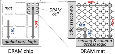
Design-induced variation in latency is present in both vertical and horizontal directions in a 2D DRAM cell array (called a mat): i) Each vertical column of cells is connected to a sense amplifier and ii) each horizontal row of cells of a mat is connected to a wordline driver. Variations in the vertical and horizontal dimensions, together, divide the cell array into heterogeneous latency regions, where cells in some regions require larger access latencies for reliable operation. This variation in latency has direct impact on the reliability of the cells. Reducing the latency uniformly across all regions in DRAM would improve performance, but can introduce failures in the inherently slower regions that require long access latencies for correct operation. We refer to these inherently slower regions of DRAM as design-induced vulnerable regions.
Our goals are to i) experimentally demonstrate, characterize and understand design-induced variation in modern DRAM chips, and ii) develop new, low-cost mechanisms that leverage design-induced variation to dynamically find and use the lowest latency at which to operate DRAM reliably, and thus improve overall system performance while ensuring reliable system operation.
We first identify the design-induced vulnerable regions of real DRAM chips. Doing so is not an easy task due to two major challenges. First, identifying design-induced vulnerable regions requires a detailed knowledge of DRAM internals. Modern DRAM cells are organized in a hierarchical manner, where cells are subdivided into multiple mats and these mats are organized as a matrix (Figure 1). Due to this hierarchical organization, the vulnerability of cells does not necessarily increase linearly with increasing row and column addresses, but depends on i) the location of the cell in the mat and ii) the location of the mat in the chip.
Second, identifying design-induced vulnerable regions is difficult due to the current DRAM interface that does not expose how data corresponding to an address is mapped inside of DRAM. Even though certain regions in DRAM might be more vulnerable due to the design and placement of cells, internal scrambling of addresses (khan-dsn2016, ) and remapping of rows and columns (liu-isca2013, ) scatters and distributes that region across the address space. In this work, we provide a detailed analysis on how to identify such vulnerable regions despite the limitations posed by the modern DRAM interface.
To understand design-induced variation in modern DRAM chips, we build an FPGA-based DRAM testing infrastructure, similar to that used by prior works (lee-hpca2015, ; kim-isca2014, ; liu-isca2013, ; chandrasekar-date2014, ; chang-sigmetrics2016, ; hassan-hpca2017, ; khan-sigmetrics2014, ; khan-cal2016, ; chang-sigmetrics2017, ; khan-dsn2016, ; chang-thesis2017, ; lee-thesis2016, ; kim-thesis2015, ). Our extensive experimental study of 96 real DIMMs (768 DRAM chips) using this infrastructure shows that i) modern DRAM chips exhibit design-induced latency variation in both row and column directions, ii) design-induced vulnerability gradually increases in the row direction within a mat and this pattern repeats in every mat, and iii) some columns are more vulnerable than others due to the internal hierarchical design of the DRAM chip.
We develop two new mechanisms that exploit design-induced variation to enable low DRAM latency at high reliability and low cost. First, we propose to reduce the DRAM latency at runtime, by dynamically identifying the lowest DRAM latency that ensures reliable operation. To this end, we develop an online DRAM testing mechanism, called DIVA Profiling. The key idea is to periodically test only the regions vulnerable to design-induced variation in order to find the minimum possible DRAM latency (for reliable operation), as these regions would exhibit failures earlier than others when the access latency is reduced and, therefore, would indicate the latency boundary where further reduction in latency would hurt reliability. DIVA Profiling achieves this with much lower overhead than conventional DRAM profiling mechanisms that must test all of the DRAM cells (nair-isca2013, ; liu-isca2012, ; venkatesan-hpca2006, ; khan-sigmetrics2014, ). For example, for a 4GB DDR3-1600 DIMM, DIVA Profiling takes 1.22ms, while conventional profiling takes 625ms.
Second, to avoid uncorrectable failures (due to lower latency) in systems with ECC, we propose DIVA Shuffling, a mechanism to reduce multi-bit failures while operating at a lower latency. The key idea is to leverage the understanding of the error characteristics of regions vulnerable to design-induced variation in order to remap or shuffle data such that the failing bits get spread over multiple ECC codewords and thereby become correctable by ECC.
We make the following contributions:
-
To our knowledge, this is the first work to experimentally demonstrate, characterize and analyze the phenomenon of design-induced variation that exists in real, state-of-the-art DRAM chips. Due to this phenomenon, when DRAM latency is reduced, we find that certain regions of DRAM are more vulnerable to failures than others, based on their relative distances from the peripheral logic.
-
We identify the regions in DRAM that are most vulnerable to design-induced variation based on the internal hierarchical organization of DRAM bitlines and wordline drivers. We experimentally demonstrate the existence of design-induced vulnerable regions in DRAM by testing and characterizing 96 real DIMMs (768 DRAM chips).
-
We develop two new mechanisms, called DIVA Profiling and DIVA Shuffling, which exploit design-induced variation to improve both latency and reliability of DRAM at low cost. DIVA Profiling is the first mechanism to dynamically determine the lowest latency at which to operate DRAM reliably: it dynamically reduces the latencies of read/write operations by 35.1%/57.8% at 55 \oldcelsius , while ensuring reliable operation. DIVA Shuffling is the first mechanism that takes advantage of design-induced variation to improve reliability by making ECC more effective: on average, it corrects 26% of total errors that are not correctable by conventional ECC, while operating at lower latency. We show that the combination of our two techniques, DIVA-DRAM, leads to a raw DRAM latency reduction of 40.0%/60.5% (read/write) and an overall system performance improvement of 14.7%/13.7%/13.8% (2-/4-/8-core) over a variety of workloads in our evaluated systems, while ensuring reliable system operation. We also show that DIVA-DRAM outperforms Adaptive-Latency DRAM (AL-DRAM) (lee-hpca2015, ), a state-of-the-art technique that lowers DRAM latency by exploiting temperature and process variation (but not designed-induced variation).222A second important benefit of DIVA-DRAM over AL-DRAM is that DIVA-DRAM is not vulnerable to changes in DRAM latency characteristics over time due to issues such as aging and wearout, since DIVA-DRAM determines latency dynamically based on runtime profiling of latency characteristics. As AL-DRAM does not determine latency dynamically and instead relies on static latency parameters, it is vulnerable to dynamic changes in latency characteristics, which leads to either potential reliability problems or large latency margins to prevent potential failures. See Section 6.1 for a more detailed discussion of this.
2. Modern DRAM Architecture
We first provide background on DRAM organization and operation that is useful to understand the cause, characteristics and implications of design-induced variation.
2.1. DRAM Organization
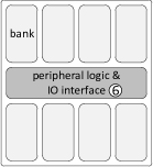
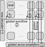
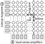
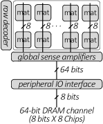
DRAM is organized in a hierarchical manner where each DIMM consists of multiple chips, banks, and mats, as shown in Figure 2. A DRAM chip (shown in Figure 2a) consists of i) multiple banks and ii) peripheral logic that is used to transfer data to the memory channel through the IO interface. Each bank (shown in Figure 2b) is subdivided into multiple mats. In a bank, there are two global components that are used to access the mats: i) a row decoder that selects a row of cells across multiple mats and ii) global sense amplifiers that transfer a fraction of data from the row through the global bitlines, based on the column address. Figure 2c shows the organization of a mat that consists of three components: i) a 2-D cell array in which the cells in each row are connected horizontally by a wordline, and the cells in each column are connected vertically by a bitline, ii) a column of wordline drivers that drive each wordline to appropriate voltage levels in order to activate a row during an access and iii) a row of local sense amplifiers that sense and latch data from the activated row.
2.2. DRAM Operation
On a memory request (e.g., to read a cache line), there are two major steps involved in accessing the requested data. First, to access a row, the memory controller issues an ACTIVATION command along with the row address to select a row in a bank. On receiving this command, DRAM transfers all the data in the row to the corresponding local sense amplifiers. Second, in order to access a specific cache line from the activated row, the memory controller issues a READ command with the column address of the request. DRAM then transfers the selected data from the local sense amplifiers to the memory controller, over the memory channel.
While this is a high-level description of the two major DRAM operations, these operations, in reality, consist of two levels of accesses through: i) global structures across mats within a bank (global sense amplifiers, global wordlines, and global bitlines) and ii) local structures within a mat (local sense amplifiers, local wordlines, and local bitlines). A row-column access goes through multiple steps in the global-local hierarchy, as annotated in Figure 2: ① When the row decoder in a bank receives a row address, it first activates the corresponding global wordline in the bank. ② The global wordline, in turn, activates the corresponding wordline driver in each mat that it is connected to. ③ The wordline driver in each mat activates the corresponding local wordline connecting the row to the local sense amplifiers. ④ These local amplifiers sense and latch the entire row through the local bitlines in each mat across the bank. ⑤ When DRAM receives the column address, a fraction of data from each mat is transferred from the local sense amplifiers to the global sense amplifiers, through the global bitlines. ⑥ Data from the global sense amplifiers is then sent to the memory channel through the IO interfaces of the DRAM chip.
Both DRAM row and column accesses are managed by issuing row and column access commands to DRAM. The minimum time between these commands is determined by internal DRAM operation considerations, such as how long it takes to sense data from cells in a selected wordline, how long it takes to transfer data from the local to the global sense amplifiers (micron-dram, ; lee-hpca2015, ; lee-hpca2013, ; kim-isca2012, ). There are four major timing parameters for managing row and column accesses. tRAS (tRP) is the minimum time needed to select (deselect) a row in a bank for activation. tRCD is the minimum time needed to access a column of a row after activating the row. tWR is the minimum time needed to update the data in a column of a row after activating the row. More detailed information on these timing parameters and DRAM operation can be found in (kim-isca2012, ; lee-hpca2015, ; lee-hpca2013, ; chang-sigmetrics2016, ).
3. Design-Induced Variation
In this work, we show that DRAM access latency varies based on the location of the cells in the DRAM hierarchy. Intuitively, transferring data from the cells near the IO interfaces (and sensing structures) incurs less time than transferring data from the cells farther away from the IO interfaces (and sensing structures). We refer to this variability in cell latency caused by the physical organization and design of DRAM as design-induced variation. Since DRAM is organized as a multi-level hierarchy (in the form of chips, banks and mats), design-induced variation exists at multiple levels. Design-induced variation has several specific characteristics that clearly distinguish it from other known types of variation observed in DRAM, e.g., process variation and temperature dependency (lee-hpca2015, ; chandrasekar-date2014, ):
-
Predetermined at design time. Design-induced variation depends on the internal DRAM design, predetermined at design time. This is unlike other types of variation, (e.g., process variation and temperature induced variation (lee-hpca2015, ; chandrasekar-date2014, )), which depend on the manufacturing process and operating conditions after design.
-
Static distribution. The distribution of design-induced variation is static, determined by the location of cells. For example, a cell closer to the sense amplifier is always faster than a cell farther away from the sense amplifier, assuming there are no other sources of variation (e.g., process variation). On the other hand, prior works show that variability due to process variation follows a random distribution (lee-hpca2015, ; chandrasekar-date2014, ), independent of the location of cells.
-
Constant. Design-induced variation depends on the physical organization, which remains constant over time. Therefore, it is different from other types of variation that change over time (e.g., variable retention time (liu-isca2013, ; khan-sigmetrics2014, ; kim-edl2009, ; qureshi-dsn2015, ; patel-isca2017, ; yaney-iedm1987, ; restle-iedm1992, ; mori-iedm2005, ), wearout due to aging (sridharan-sc2012, ; sridharan-sc2013, ; meza-dsn2015, ; schroeder-tdsc2010, ; li-atc2007, ; hwang-asplos2012, ; wee-jssc2000, ; min-vlsi2001, ; tanabe-jssc1992, )).
-
Similarity in DRAMs with the same design. DRAMs that share the same internal design exhibit similar design-induced variation (Section 5.3). This is unlike process variation that manifests itself significantly differently in different DRAM chips with the same design.
The goals of this work are to i) experimentally demonstrate, characterize, and understand the design-induced variation in real DRAM chips, especially within and across mats, and ii) leverage this variation and our understanding of it to reduce DRAM latency at low cost in a reliable way. Unfortunately, detecting the design-induced vulnerable regions is not trivial and depends on two factors: i) how bitline and wordline drivers are organized internally, ii) how data from a cell is accessed through the DRAM interface. In order to define and understand the design-induced variation in modern DRAM, we investigate three major research questions related to the impact of DRAM organization, interface, and operating conditions on design-induced variation in the following sections.
3.1. Impact of DRAM Organization
The first question we answer is: how does the DRAM organization affect the design-induced vulnerable regions? To answer this, we present i) the expected characteristics of design-induced variation and ii) systematic methodologies to identify these characteristics in DRAM chips.
Effect of Row Organization. As discussed in Section 2.1, a mat consists of a 2D array of DRAM cells along with peripheral logic needed to access this data. In the vertical direction, DRAM cells (typically, 512 cells (vogelsang-micro2010, ; kim-isca2012, )), connected through a bitline, share a local sense amplifier. As a result, access latency gradually increases as the distance of a row from the local sense amplifier increases (due to the longer propagation delay through the bitline). This variation can be exposed by reading data from DRAM faster by using smaller values for DRAM timing parameters. Cells in the rows closer to the local sense amplifiers can be accessed faster in a reliable manner. Hence, they exhibit no failures due to shorter timing parameters. On the contrary, cells located farther away from the sense amplifiers take longer to access in a reliable manner, and might start failing when smaller values are used for the timing parameters. As a result, accessing rows in ascending order starting from the row closest to the sense amplifiers should exhibit a gradual increase in failures due to design-induced variation, as shown in Figure 3a. In this figure, the darker color indicates slower cells, which are more vulnerable to failures when we reduce the access latency.
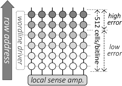
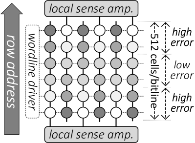
In the open-bitline scheme (inoue-jssc1988, ), alternate bitlines within a mat are connected to two different rows of sense amplifiers (at the top and at the bottom of the mat), as shown in Figure 3b. In this scheme, even cells and odd cells in a row located at the edge of the mat exhibit very different distances from their corresponding sense amplifiers, leading to different access latencies. On the other hand, cells in the middle of a mat have a similar distance from both the top and bottom sense amplifiers, exhibiting similar latencies. Due to this organization, we observe that there are more failures in rows located on both ends of a mat, but there is a gradual decrease in failures in rows in the middle of the mat.
Based on these observations about row organization, we define two expected characteristics of vulnerable regions across the rows when we reduce DRAM latency uniformly. First, the number of failures would gradually increase with increased distance from the sense amplifiers. Second, this gradual increase in failures would periodically repeat in every mat (every 512 rows). We experimentally demonstrate these characteristics in Section 5.1.
Effect of Column Organization. As we discussed in Section 2.2, the wordline drivers in DRAM are organized in a hierarchical manner: a strong global wordline driver is connected to all mats over which a row is distributed and a local wordline driver activates a row within a mat. This hierarchical wordline organization leads to latency variation at two levels. First, a local wordline in a mat located closer to the global wordline driver starts activating the row earlier than that in a mat located farther away from the global wordline driver (design-induced variation due to the global wordline). Second, within a mat, a cell closer to the local wordline driver gets activated faster than a cell farther away from the local wordline driver (design-induced variation due to the local wordline). Therefore, columns that have the same distance from the local wordline driver, but are located in two different mats, have different latency characteristics (see Figure 4, where a darker color indicates slower cells, which are more vulnerable to failures if/when we reduce the access latency). However, exact latency characteristics of different columns in different mats depend on the strength of the global versus local wordline drivers and the location of the respective mats and columns.

We define two expected characteristics of vulnerable regions across columns when we reduce DRAM latency uniformly. First, although some columns are clearly more vulnerable than others, the number of failures likely would not gradually increase with ascending column numbers. Second, the failure characteristics observed with ascending column numbers would be similar for all rows. We experimentally demonstrate these characteristics in Section 5.2.
3.2. Impact of the Row/Column Interface
Our second question is: how does the row/column interface affect the ability to identify the design-induced vulnerable regions in DRAM? Unfortunately, identifying design-induced vulnerable regions becomes challenging due to a limited understanding of how data corresponding to an address is mapped inside DRAM. While it is possible to identify vulnerable regions based on location, exposing and exploiting such information through the row/column DRAM addressing interface is challenging due to two reasons.
Row Interface (Row Address Mapping). DRAM vendors internally scramble the row addresses in DRAM. This causes the address known to the system to be different from the actual physical address (vandegoor-delta2002, ; khan-dsn2016, ; liu-isca2013, ). As a result, consecutive row addresses issued by the memory controller can be mapped to entirely different regions of DRAM. Unfortunately, the internal mapping of the row addresses is not exposed to the system and varies across products from different generations and manufacturers. In Section 3.1, we showed that if the access latency is reduced, accessing rows in a mat in ascending row number order would exhibit a gradual increase in failures. Unfortunately, due to row remapping, accessing rows in ascending order of addresses known to the memory controller will likely exhibit irregular and scattered failure characteristics.
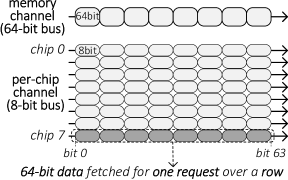
Column Interface (Column Address Mapping). In the current interface, the bits accessed by a column command are not mapped to consecutive columns in a mat. This makes it challenging to identify the vulnerable regions in a wordline. When a column address is issued, 64 bits of data from a row are transferred over the global bitlines (typically, 64-bit wide (vogelsang-micro2010, )). This data is transferred in eight 8-bit bursts over the IO channel, as shown in Figure 5. However, the data transferred with each column address comes from cells that are in different mats, and have different distances from their global and local wordline drivers. This makes it impossible to determine the physical column organization by simply sweeping the column address in ascending order.
In this work, we provide alternate ways to identify design-induced vulnerable regions using the current row/column interface in DRAM. We describe the key ideas of our methods.
-
Inferring vulnerable rows from per-row failure count. In order to identify the gradual increase in design-induced variability with increasing row addresses in mats (in terms of internal DRAM physical address), we try to reverse engineer the row mapping in DRAM. We hypothesize the mapping for one mat and then verify that mapping in other DRAM mats in different chips that share the same design. The key idea is to correlate the number of failures to the physical location of the row. For example, the most vulnerable row would be the one with the most failures and hence should be located at the edge of the mat. Section 5.3 provides experimental analysis and validation of our method.
-
Inferring vulnerable columns from per-bit failure count in the IO channel. A column access transfers 64 bits of data from a DRAM chip over the IO channel. These 64 bits come from 64 bitlines that are distributed over different mats across the entire row. Our key idea to identify the vulnerable bitlines in the column direction is to examine each bit in a 64-bit burst. We expect that due to design-induced variation, some bits in a 64-bit burst that are mapped to relatively slow bitlines are more vulnerable than other bits. In Section 5.4, we experimentally identify the location of bits in bursts that consistently exhibit more failures, validating the existence of design-induced variation in columns.
3.3. Impact of Operating Conditions
The third question we answer is: Does design-induced variation in latency show similar characteristics at different operating conditions? DRAM cells get affected by temperature and the refresh interval (lee-hpca2015, ; liu-isca2013, ; khan-sigmetrics2014, ; patel-isca2017, ). Increasing the temperature within the normal system operating range (45 \oldcelsius to 85 \oldcelsius ) or increasing the refresh interval increases the leakage in cells, making them more vulnerable to failure. However, as cells get similarly affected by changes in operating conditions, we observe that the trends due to design-induced variation remain similar at different temperatures and refresh intervals, even though the absolute number of failures may change. We provide detailed experimental analysis of design-induced variation at different operating conditions, in Section 5.5.
4. DRAM Testing Methodology
In this section, we describe our FPGA-based DRAM testing infrastructure and the testing methodology we use for our experimental studies in Section 5.
FPGA-Based DRAM Testing Infrastructure. We build an infrastructure similar to that used in previous works (lee-hpca2015, ; kim-isca2014, ; liu-isca2013, ; chandrasekar-date2014, ; chang-sigmetrics2016, ; hassan-hpca2017, ; khan-dsn2016, ; khan-sigmetrics2014, ; chang-sigmetrics2017, ; khan-cal2016, ; kim-thesis2015, ; lee-thesis2016, ; chang-thesis2017, ). Our infrastructure provides the ability to: i) generate test patterns with flexible DRAM timing parameters, ii) provide an interface from a host machine to the FPGA test infrastructure, and iii) maintain a stable DRAM operating temperature during experiments. We use a Xilinx ML605 board (ml605, ) that includes an FPGA-based memory controller connected to a DDR3 SODIMM socket. We designed the memory controller (mig, ) with the flexibility to change DRAM parameters. We connect this FPGA board to the host machine through the PCIe interface (pcie, ). We manage the FPGA board from the host machine and preserve the test results in the host machine’s storage. In order to maintain a stable operating temperature for the DIMMs, during our experiments, we place the FPGA board in a heat chamber that consists of a temperature controller, a temperature sensor, and a heater which enables us to test at different temperatures.
Profiling Methodology. The major purpose of our experiments is to characterize design-induced variation in DRAM latency. We would like to i) determine the characteristics of failures when we reduce timing parameters beyond the error-free operation region, and ii) observe any correlation between the error characteristics and the internal design of the tested DRAMs. To this end, we analyze the error characteristics of DRAM by lowering DRAM timing parameters below the values specified for error-free operation.
An experiment consists of three steps: i) writing background data, ii) changing timing parameters, and iii) verifying cell content. In Step 1, we write a certain data pattern to the entire DIMM with standard DRAM timing parameters, ensuring that correct (i.e., the intended) data is written into all cells. In Step 2, we change the timing parameters. In Step 3, we verify the content of the DRAM cells after the timing parameters are changed. To pass verification, a DRAM cell must maintain its data value until the next refresh operation. To complete the verification step, we let DRAM cells remain idle and leak charge for the refresh interval and read and verify the data. If the data read in Step 3 does not match the data written in Step 1, we log the addresses corresponding to the failures and the failed bits in the failed addresses.
Data Patterns. In order to exercise worst-case latency behavior, we use a row stripe pattern, wherein a test pattern is written in odd rows and an inverted test pattern is written in even rows (vandegoor-delta2002, ; kim-isca2014, ). This pattern drives the bitlines in opposite directions when accessing adjacent rows. The patterns we have used in our tests are 0000, 0101, 0011, and 1001. We perform the test twice per pattern, once with the test data pattern and once with the inverted version of the test data pattern, in order to test every cell in charged (e.g., data 1) and non-charged states (e.g., data 0). We report the sum of failures from these two cases for each test. We perform 10 iterations of the same test to make sure the errors are consistent.
We evaluate four DRAM timing parameters: tRCD, tRAS, tRP, and tWR. For each timing parameter, our evaluations start from the standard values (13.75/35.0/13.75/15.0ns for tRCD/tRAS/tRP/tWR, respectively) (micron-dram, ) and reduce the timing parameters to the lowest values that our DRAM infrastructure allows (5ns for tRCD/tRAS/tWR, and tRCD + 10ns for tRAS). We use 96 DIMMs, comprising 768 DRAM chips, from three DRAM vendors for our experiments. Appendix D lists evaluated DIMMs and their major characteristics. We provide detailed results for each DIMM online (safari-git, ).
5. Characterization of Design-Induced Variation in DRAM
In this section, we present the results of our profiling studies that demonstrate the presence of design-induced variation in both the vertical (bitline) and horizontal (wordline) directions. We i) show the existence of design-induced variation in Sections 5.1 and 5.2, ii) analyze the impact of the row and column interface in Sections 5.3 and 5.4, and iii) characterize the impact of operating conditions on design-induced variation in Section 5.5. We then provide a summary of our analysis on design-induced variation across 96 DIMMs (768 DRAM chips) in Section 5.6. In Appendix B, we present the results of our supporting circuit-level SPICE simulation studies that validate our hypotheses on design-induced variation in a mat.
5.1. Design-Induced Variation in Bitlines
As we explain in Section 3.1, we expect different error characteristics for different cells connected to a bitline, depending on the relative distances of the cells from the local sense amplifiers. To demonstrate the existence of design-induced variation in a bitline, we design a test pattern that sweeps the row address.
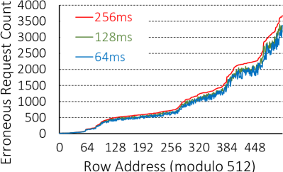
Per-Row Error Count with Row Address Sweeping. Figure 6 plots the error count for four values of a DRAM timing parameter, tRP (whose standard value is 13.75ns), with a refresh interval of 256 ms (greater than the normal 64 ms refresh interval to emphasize the effects of access latency (lee-hpca2015, )) and an ambient temperature of 85 \oldcelsius . We tested all rows (and 16 columns) in a DIMM and plot the number of erroneous accesses for each set of row address modulo 512 rows.333Even though there are redundant cells (rows), DRAM does not allow direct access to redundant cells. Therefore, we can only access a 512512 cell mat ( data chunk). Figure 6 plots the number of erroneous requests in every 512-cell chunk. We aggregate the error count across errors every set of row address modulo 512 rows because each bitline is connected to 512 cells. Hence, our expectation is that the design-induced variation pattern will repeat every 512 cells.444Note that Figure 6 shows the sum of all error counts for all rows with the same row number modulo 512. In other words, each value on the x-axis of Figure 6c represents a modulo value i, where the corresponding y-axis value shows the aggregated number of errors for the set of rows – Row i, Row 512+i, Row 1024+i, etc. We provide each individual row’s error count in Figure 7b to substantiate this further. We make two key observations. First, reducing a timing parameter enough below its standard value induces errors, and reducing it further induces more errors. At a tRP of 12.5ns, there are no errors, due to the latency margin that exists in DRAM cells, as shown in previous works (lee-hpca2015, ; chang-sigmetrics2016, ). At a tRP of 10.0ns (3.75ns reduction from the standard value), the number of errors is small, as shown in Figure 6b while at a tRP of 5.0ns, we observe a large number of errors, as shown in Figure 6d. Second, we observe significant error count variation across 512 row chunks only at 7.5ns (with error counts ranging from 0 to more than 3500 in Figure 6c), while most errors are randomly distributed at 10.0ns (Figure 6b) and most rows show very high error counts at 5.0ns (Figure 6d).


Periodicity in Per-Row Error Count. To understand these trends better, we break down the error counts further for a tRP of 7.5ns. As we expect the variation pattern to repeat every 512 rows, we use the value of row address modulo 512 (which we refer to as a row chunk) to tally all of the number of errors observed in the DIMM, as shown in Figure 6c. We then sort the row chunks based on the number of errors, shown in Figure 7a. To see whether periodicity exists, we then reorder the erroneous request counts of each individual row within every set of 512 rows by using the sorted order in Figure 7a, which we show in Figure 7b. We reorder the per-row data in this manner as, without the sorting, it is difficult to observe the periodicity that exists in the error count.
As expected, there is periodicity in error counts across 512 row chunks. Therefore, we conclude that error count shows periodicity with row address, confirming our expectation that there is predictable design-induced variation in the latency of cells across a bitline. We will understand the reason why this periodicity does not show up with increasing row addresses in Section 5.3.


5.2. Design-Induced Variation in Wordlines
As we explained in Section 3.1, we expect design-induced variation across cells in a wordline, depending on the distance from the wordline driver. To confirm the existence of design-induced variation across a wordline, we use a similar evaluation methodology as the one used in Section 5.1, except that i) we sweep the column address instead of the row address, ii) aggregate errors in the same column across multiple rows (128 columns per row). In order to minimize the impact of variation across a bitline and focus on variation across a wordline, we test all columns in only 16 rows.
Per-Column Error Count with Column Address Sweeping. Figure 8 provides results with two tRP values (10ns and 7.5ns). Similar to the evaluation with sweeping row addresses, we see that the number of errors is small and the distribution is random when tRP is reduced by a small amount, as shown in Figure 8a. However, the number of errors is large when tRP is reduced significantly, as shown in Figure 8b. We observe variations in error counts across different column addresses at a tRP of 7.5ns. Besides other variations, there is a large jump near the 48th column and a dip in error count near the 96th column, as shown in Figure 8b.


To understand these, we separately plot each row’s error count, which displays different patterns. We provide two such types of patterns (obtained from multiple rows) in Figures 8c and 8d. In one such type, shown in Figure 8c, the error count drastically increases at around the 80th column and drops at around the 96th column (There are other types of patterns with similar shapes but with the jumps/drops happening at different locations). In the type of pattern shown in Figure 8d, the error count drastically increases at the 96th column and stays high. We attempt to correlate such behavior with the internal organization of DRAM.
Figure 9 shows an illustration of how the precharge control signal flows across mats. The timing parameter tRP dictates how long the memory controller should wait after it issues a precharge command before it issues the next command. When a precharge command is issued, the precharge signal propagates to the local sense amplifiers in each mat, leading to propagation delay (higher for sense amplifiers that are farther away). To mitigate this variation in the delay of the precharge control signal, DRAM uses two signals, i) a main precharge signal – propagating from left to right, and ii) a sub precharge signal – that directly reaches the right and propagates from right to left.
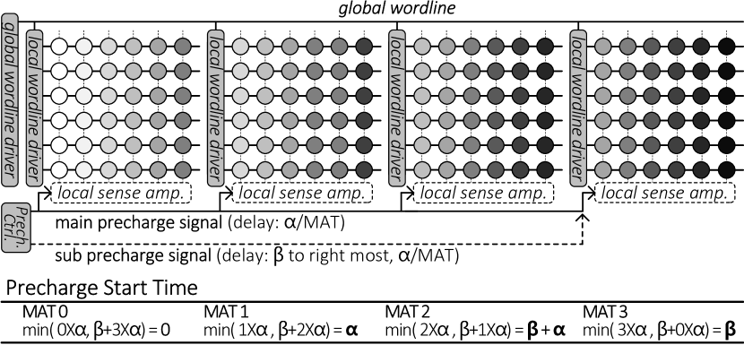
The main and sub precharge signals arrive at different times at the different mats due to parasitic capacitance on the propagation path. The main precharge signal is delayed by per mat going from left to right, while the sub precharge signal is delayed by when it reaches the rightmost mat where , since the sub precharge signal does not have any load going from left to right. However, after that, the sub precharge signal exhibits a delay of per mat when propagating through mats from right to left. The sense amplifiers in a mat respond to the faster one of the two precharge signals. For instance, in Figure 9, mat 3 receives the precharge signal the last. Hence, accesses to it would exhibit more errors than accesses to other mats if tRP is reduced. Such control signal delays result in the kind of jumps in errors at particular column addresses we see in real DRAM chips (e.g., Figures 8b, 8c, 8d). We conclude that error count varies across columns, based on the column’s distance from the wordline and control signal drivers. While such control signal delays explain why such jumps occur, knowledge of the exact location of mats and how they are connected to the control signals is necessary to understand and explain why jumps occur at particular column addresses.
5.3. Effect of the Row Interface
As shown in Figure 6c, the error count across a bitline does not linearly increase with increasing DRAM-external row address (i.e., the address issued by the memory controller over the memory channel). However, we observe periodicity when rows are sorted by error count, as shown in Figure 7. This behavior could occur because the DRAM-external row address is not directly mapped to the internal row address in a DRAM mat (liu-isca2013, ). Without information on this mapping, it is difficult to tie the error count periodicity to specific external row addresses. In this subsection, we estimate the most-likely mapping between the DRAM-external row address and the DRAM-internal row address (estimated row mapping) based on the observed error count. We then analyze the similarity of the estimated row address mapping across multiple DIMMs manufactured by the same DRAM company (in the same time frame).
Methodology for Estimating Row Address Mapping. We explain our estimation methodology using a simple example shown in Figure 10, which has a 3-bit row address (eight rows per mat). Figure 10a shows the DRAM-internal row address in both decimal and binary, increasing in the order of distance between the row and the sense amplifier.
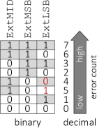
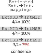
Figure 10b shows DRAM-external row addresses that are ranked based on the error counts. As observed, the order is not the same as the DRAM-internal address order in Figure 10a. To determine the estimated external-to-internal row mapping based on the observed error counts for the external addresses, we explore all possible permutations that rearrange the three bits in the row address. For each of the eight rows in the mat, we have the error count. Our goal is to find an ordering of the three bits, which we call the internal row address, for which the error count monotonically increases with the number represented by the three bits. For example, after rearranging, the row with an internal row address of “001” should have a higher error count than the row with an internal row address of “000”. We find that by mapping the MSB of the internal row address (IntMSB) to the middle bit of the external row address (ExtMID), and by mapping the middle bit of the internal row address (IntMID) to the MSB of the external row address (ExtMSB), as shown in Figure 10c, the row error count increases monotonically with the internal row address. The estimated mapping (in the logical address) is indicated by dark boxes when the expected bit is “1” and light boxes when the expected bit is “0”. There are cases when this mapping does not match with the actual external address (indicated in red). Figure 10c shows that, in this example, external to internal mapping can be estimated with high confidence. For example, we can say with 100% confidence that the external address bit ExtMID maps to the internal address bit IntMSB since the observed error counts for the ExtMID bit match the expected error counts from the IntMSB bit.
Estimated Row Address Mapping in Real DIMMs. We perform such an external to internal address mapping comparison and mapping exercise on eight DIMMs manufactured by the same company in a similar time frame. Figure 11 shows the average confidence level over all rows in a DIMM, for the estimated row mapping. We use error bars to show the standard deviation of the confidence over eight DIMMs. We make three observations. First, all DIMMs show the same estimated row mapping (with fairly high confidence) for at least the five most significant bits. This result shows that DIMMs manufactured by the same company at the same time have similar design-induced variation. Second, the confidence level is almost always less than 100%. This is because process variation and row repair mechanisms introduce perturbations in addition to design-induced variation, which can change the ranking of rows (determined based on error counts as we explained earlier). Third, the confidence level drops gradually from IntMSB to IntLSB. This is also due to the impact of process variation and row repair mechanisms. The noise from process variation and row repair can change row ranking and grouping by error count. Address bits closer to IntMSB tend to divide rows into groups at a larger granularity than address bits closer to IntLSB. Therefore, the higher order bits show higher confidence. Based on these observations, we conclude that DRAMs that have the same design display similar error characteristics due to design-induced latency variation.

In summary, we observe predictable row address mapping (similar to Figure 11) when testing DIMMs from the same vendor that were manufactured around the same time frame (i.e., they likely have the same internal circuit design).
5.4. Effect of the Column Interface
Another way to observe the error characteristics in the wordline organization is by using the mapping between the global sense amplifier and the IO channel. As we explained, global sense amplifiers in a DRAM chip concurrently read 64-bit data from different locations of a row, leading to variation in errors. Figure 12 plots errors in 64-bit data-out (as shown in Figure 5) in the IO channel (For example, first eight bits (bits 0 – 7) are the first burst of data transfer). We draw three conclusions. First, there is large variation in the amount of errors in the IO channel. For example, more than 26K errors happen in the third bit while no errors are observed in the first bit of the IO channel. Second, the error characteristics of eight DRAM chips show similar trends. Third, while we observed regular error distribution at different bit positions from DIMMs that show design-induced variation, we also observed that the error patterns from different DIMMs (e.g., DIMMs from different vendors) were different. Section 6.2 uses these observations to develop a new error correction mechanism, called DIVA Shuffling.

5.5. Effect of Operating Conditions
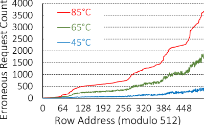
Figure 13 shows the error count sensitivity to the refresh interval and the operating temperature by using the same method as row sweeping (aggregating the error count across every set of row address modulo 512 rows, as done in Section 5.1). We make three observations. First, neither the refresh interval nor temperature changes the overall trends of design-induced variation (i.e., the variability characteristics in different row addresses remain the same, though the absolute number of errors changes). Second, reducing the refresh interval or the ambient temperature within the normal system operating conditions (i.e., 45 \oldcelsius to 85 \oldcelsius ) leads to fewer errors. Third, the variability in cells is much more sensitive to the ambient temperature than the refresh interval. When changing the refresh interval, the total error count does not change drastically: it exhibits only a 15% decrease with a 4X reduction in refresh interval. On the other hand, changing the ambient temperature has a large impact on the total error count: error count reduces by 90% with a 40 \oldcelsius change in temperature. This is due to the fact that frequent refreshes make only the cells faster (lee-hpca2013, ; hassan-hpca2016, ; shin-hpca2014, ), whereas reducing temperature makes not only the cells but also the peripheral circuits faster. Based on these observations, we conclude that temperature or refresh interval do not change the trends in design-induced variation, but they impact the total number of failures in vulnerable regions at different rates.
5.6. Summary Results of 96 DIMMs
We profile 96 DIMMs with 768 chips from three vendors to characterize the design-induced variation in DRAM chips. We observe similar trends and characteristics in DIMMs from the same generation, though the absolute number of failures are different. In Figure 14, we show the error count difference between the most vulnerable region vs. the least vulnerable region in each of the tested DIMMs. We define the difference as vulnerability ratio and calculate it using the error count ratio between the error count of the top 10% most vulnerable rows and the error count of the top 10% least vulnerable rows.555Note that the results show the variation of error distribution, which does not represent either the performance or the reliability of DIMMs from different vendors.
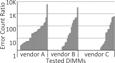
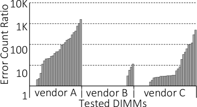
We make two observations from this figure. First, most of the DIMMs exhibit large design-induced variation in terms of vulnerability ratio (e.g., as high as 5800 times, notice the log scale). Second, we did not observe design-induced variation in 24 DIMMs. However, we believe that this is in part due to a limitation of our infrastructure, where we can reduce timing parameters only at a coarser granularity (i.e., at a step size of 2.5 ns) due to the limited FPGA frequency, similar to the DRAM test infrastructures used in prior works (lee-hpca2015, ; kim-isca2014, ; chandrasekar-date2014, ; liu-isca2013, ; hassan-hpca2017, ; chang-sigmetrics2016, ; khan-sigmetrics2014, ; khan-dsn2016, ; chang-sigmetrics2017, ; khan-cal2016, ; kim-thesis2015, ; lee-thesis2016, ; chang-thesis2017, ). As a result, it is sometimes possible that reducing a step of a timing parameter causes the tested DIMM to transition from a no-error or very-low-error state to a state where latency is low enough to make all cells fail, missing the timing where design-induced variation is clearly visible. In real machines where state-of-the-art DRAM uses a much lower clock period (e.g., DDR3-2133: 0.94ns), design-induced variation might be prevalent. Third, DRAMs from the same vendor and from similar production time frames show similar characteristics to each other, including whether or not they are susceptible to design-induced variation related errors. For example, DRAMs from Vendor B have drastically high error counts across most regions when tRCD is reduced below a certain value. We include summary results for each DIMM that we tested in Appendix D. We provide detailed results for each DIMM online (safari-git, ).
In summary, we have experimentally demonstrated that i) design-induced variation is prevalent across a large number of DIMMs and ii) our observations hold true in most of the DIMMs. We validate these observations on the existence of design-induced variation in DRAM using circuit-level SPICE simulations in Appendix B. We conclude that modern DRAMs are amenable to reducing latency by exploiting design-induced variation.
6. Mechanisms to Exploit Design-Induced Variation
In this section, we present two mechanisms that leverage design-induced variation to reduce DRAM latency while maintaining reliability: i) Design-Induced Variation Aware online DRAM Profiling (DIVA Profiling) to determine by how much DRAM latency can be safely reduced while still achieving failure-free operation, and ii) Design-Induced Variation Aware data Shuffling (DIVA Shuffling) to avoid uncorrectable failures (due to lower latency) in systems with ECC. We intentionally aim to design intuitive and simple mechanisms, such that they are practical and easy to integrate into real systems.
6.1. DIVA Profiling
Previous works observe that the standard DRAM timing parameter values are determined based on the worst-case impact of process variation and worst-case operating conditions, and leverage this observation to reduce overall DRAM latency under common-case operating conditions (lee-hpca2015, ; chandrasekar-date2014, ). We leverage design-induced variation in DRAM to develop a dynamic and low-cost DRAM latency/error profiling technique. We call this technique Design-Induced Variation Aware Online DRAM Profiling (DIVA Profiling). The key idea is to separate reduced-latency-induced errors into two categories, one caused by design-induced variation and the other caused by process variation, and then employ different error mitigation techniques for these two error categories.
DIVA Profiling avoids two shortcomings faced by prior work on exploiting latency variation to reduce overall DRAM latency (lee-hpca2015, ; chandrasekar-date2014, ). These prior works, which do not exploit design-induced latency variation, are unable to perform effective online profiling to dynamically determine DRAM latency, since online profiling can incur high performance overhead (singh-mtdt2005, ; elm-mtdt1994, ; rahman-prdc2011, ; patel-isca2017, ). As a result, these prior works rely on static profiling, which leads to two key shortcomings. First, prior works do not present any concrete way to identify the lowest possible values of timing parameters that guarantee reliability. Second, these works do not account for dynamic changes in minimum DRAM latency that happen over time due to circuit aging and wearout. Therefore, implementable mechanisms based on these works have to assume conservative margins to ensure reliable operation in the presence of aging and wearout. This causes the realistic latency reductions with such mechanisms to be lower than what we optimistically show for these mechanisms (lee-hpca2015, ) in our evaluations (Section 6.3). By employing low-cost online profiling, DIVA Profiling can attain much more aggressive latency reductions while maintaining reliable operation.666Note that our evaluation of AL-DRAM does not factor in dynamic latency increases due to aging and wearout, giving AL-DRAM an unfair advantage in our results, overestimating its latency benefit.
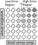
Design-Induced Variation vs. Process Variation. The error characteristics from process variation and design-induced variation are very different. Figure 15 shows the error patterns from these two types of variation (darker cells are more error prone). First, the errors caused by process variation are usually randomly distributed over the entire DRAM chip (lee-hpca2015, ; chandrasekar-date2014, ) (Figure 15a). Because these errors are random, existing ECC mechanisms (e.g., SECDED) (meza-dsn2015, ; luo-dsn2014, ) can detect and recover these random errors. On the other hand, the errors caused by design-induced variation are more systematic and are concentrated in specific regions in the DRAM chip (Figure 15b). For instance, when timing parameters are aggressively reduced, cells that are farther away from both the row driver and the local sense amplifiers are prone to more errors. As these high-error cells are concentrated on a specific region of the mat, they typically result in multi-bit errors that cannot be corrected by simple ECC (e.g., SECDED). To avoid these undesirable multi-bit errors, we propose to periodically profile only the high-error (i.e., vulnerable) regions and track whether any of these regions fail under a specific set of timing parameters, which incurs much less overhead than profiling the entire DRAM, and then tune the timing parameters appropriately based on the failure information.

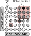
DIVA Profiling Mechanism. DIVA Profiling combines SECDED ECC, which stores ECC codewords in a separate chip on the DIMM (similar to commodity DRAM), with online profiling in a synergistic manner to reduce DRAM latency while maintaining high reliability. Due to design-induced variation, there is a specific region within each subarray of the DRAM that requires the highest access latency in the subarray. The DIVA-profiling-based memory system uses this slowest region, which we call the latency test region, to perform online latency profiling. To address the random effect of process variation across different subarrays in the entire DRAM chip, our mechanism employs per-subarray latency test regions.777We further discuss the effect of process variation in Appendix C.
Note that actual useful data (e.g., application or system data) is not stored in these per-subarray latency test regions. A memory controller with DIVA Profiling support periodically accesses these latency test regions and determines the smallest value of DRAM timing parameters required for reliable operation in all of the latency test regions (without causing multi-bit errors). The system then adds a small margin to the timing parameters obtained from this profiling (e.g., one clock cycle increase) to determine the timing parameters for the other regions (data region), which store the actual useful data required by the system and the programs.
System Changes to Enable DIVA Profiling. We require three changes to the system. First, we need to account for the repair/remapping process employed by DRAM vendors to increase yield. As we describe in Section 3.2, when faulty cells are identified during post-manufacturing test, the rows or columns corresponding to these faulty cells are remapped to other rows or columns by blowing fuses after manufacturing (arndt-iemt1999, ). If a row from the latency test region is remapped to a different row, this will affect the profiling phase of our mechanism. In order to avoid such interactions with the repair/remapping process (and potential inaccuracies in identification of the lowest latency at which to operate a DRAM chip reliably), we propose an approach where rows from the latency test regions are not remapped by DRAM vendors. Faulty cells in the latency test region are instead repaired using column remapping, another repair mechanism that is already implemented in commercial DRAM (horiguchi-book, ). Our mechanism finds a uniform latency for an entire DIMM, at which all rows in all latency test regions of the DIMM operate reliably, by selecting the smallest latency that guarantees reliable operation of all such test rows. Therefore, the profiled latency can be used to reliably operate all non-test rows (both normal rows and redundant rows). This approach is straightforward to implement, since DRAM vendors are likely to know the most vulnerable regions in the DRAM chip (based on their design knowledge). Since rows in the latency test regions do not store any useful data, this approach maintains system reliability.
Second, systems with DIVA Profiling require the ability to change DRAM timing parameters online. Since DIVA Profiling uses only one set of timing parameters for the entire DIMM, the only required change is updating the timing parameters in the memory controller with the smallest latency values that still ensure reliable operation.
Third, DIVA Profiling requires a way of exposing the design-induced variation to the memory controller. The most intuitive approach is to expose either the internal organization or the location of the slowest region as part of the DRAM specification or the SPD (Serial Presence Detect) data in DIMMs (e.g., as done in (kim-isca2012, ; chang-sigmetrics2016, ; lee-hpca2013, )). Address scrambling techniques in the memory controller need not impact DIVA Profiling since memory controller i) knows how the addresses are scrambled, and ii) can generate requests for profiling without applying scrambling.
DIVA Profiling Overhead. There are several overheads to consider when implementing DIVA Profiling. First, in terms of area overhead within the DRAM array, DIVA Profiling reduces the memory capacity slightly by reserving a small region of the DRAM for latency testing. In a conventional DRAM, which typically contains 512 rows per subarray, the area overhead is 0.2% (one row per subarray). Second, in terms of latency overhead, DIVA Profiling requires additional memory accesses, which could potentially delay demand memory requests. However, we expect the latency overhead of profiling to be low, since DIVA Profiling reserves only the slowest rows as the test region (one row per subarray), and only these rows need to be profiled. DIVA Profiling is much faster than conventional online profiling mechanisms that must test all of the DRAM cells (nair-isca2013, ; liu-isca2012, ; venkatesan-hpca2006, ; khan-sigmetrics2014, ): DIVA Profiling takes 1.22ms per data pattern888A DRAM manufacturer can select and provide the worst-case data pattern(s) DIVA Profiling should use for each DRAM module. This information can be conveyed via the Serial Presence Detect (SPD) circuitry present in each DRAM module (as done in (kim-isca2012, ; chang-sigmetrics2016, ; lee-hpca2013, )). to profile a 4GB DDR3-1600 DIMM, whereas conventional profiling takes 625ms (see Appendix A for the detailed calculation). We can employ intelligent and optimized profiling mechanisms that can further reduce the impact of the overhead. For example, one simple and low overhead mechanism can conduct online profiling as part of the DRAM refresh operation (e.g., similar to methods that parallelize refresh operations and memory accesses (chang-hpca2014, )), which would have minimal effect on memory system performance. Third, in terms of storage overhead within the memory controller, systems with DIVA Profiling require a very small amount of additional storage (e.g., as low as 16 bits for a 4GB DIMM) to implement the profiling mechanism: one bit per DIMM to track if any rows fail for the current timing parameters being tested, and one row address register per DIMM, which points to the slowest region in the DIMM.
In summary, our mechanism profiles only the slowest region that is most affected by design-induced variation, thereby incurring low profiling overhead, while achieving low DRAM latency and high reliability.
Energy Consumption. DIVA Profiling consumes similar energy for a single DRAM operation (e.g., activation, read, write, and precharge) compared to conventional DRAM. The profiling overhead is low since only the test region needs to be profiled. Furthermore, the DRAM latency reductions enabled by DIVA Profiling reduces system execution time, as we will see in Section 6.3, and can thereby reduce system energy consumption.
Other Sources of Latency Variation in DRAM. DIVA Profiling has been designed with careful consideration of other sources of DRAM latency variations, e.g., voltage (due to supply grid) & temperature variation and VRT (Variable Retention Time (liu-isca2013, ; khan-sigmetrics2014, ; kim-edl2009, ; qureshi-dsn2015, ; patel-isca2017, ; yaney-iedm1987, ; restle-iedm1992, ; mori-iedm2005, )). As explained, we divide DRAM failures into two categories: i) localized, systematic failures (caused by design-induced variation); and ii) random failures (caused by process variation and VRT). We then exploit different error mitigation techniques to handle these two different categories of failures: i) online profiling for localized systematic failures, and ii) ECC for random failures. Since the physical size of a mat is very small (e.g., 1415.6 in 30 nm technology), the effects of voltage and temperature variation are similar across a mat. The negative effects of process variation and VRT can be handled by ECC. Furthermore, we tackle the impact of sense amplifier offset (i.e., the phenomenon that a sense amplifier shows different sensitivities for detecting “0” and “1” due to process variation (keeth-book, )) by profiling all columns of the rows in all latency test regions. Hence, the variation from sense amplifier offset is accounted for in determining the smallest possible values of timing parameters that ensure reliable operation.
There can be several opportunities for applying different timing parameters to exploit process variation (e.g., variation across subarrays, variation across banks, or variation across chips). DIVA Profiling, for example, can be used to determine different timing parameters for different subarrays, banks, or chips within a DIMM. While exploiting the latency variation induced by process variation in such a manner is promising, we leave this for future work.999A recent work (chang-sigmetrics2016, ; chang-thesis2017, ) characterizes and exploits this type of process variation, providing promising results. In DIVA-DRAM, we focus solely on exploiting design-induced variation, which remains consistent across DRAM chips. To this end, DIVA Profiling uses the same timing parameters across all chips in a DIMM.
6.2. DIVA Shuffling
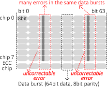
Our second approach focuses on leveraging design-induced variation to mitigate uncorrectable errors in memory systems with ECC (especially when DRAM is operated at a lower latency than the standard latency). As we observed in Section 5.4, when data is read out of a memory channel, data in specific locations tends to fail more frequently. This happens because data is delivered from locations that are distributed across a wordline. Due to design-induced variation in wordline and control signals, it takes longer to access cells in specific locations compared to cells in other locations, which could lead to multi-bit errors in memory systems with ECC. Figure 16a shows the effect of design-induced variation in systems with ECC. Data in the darker grey regions (high-error bits) tends to be more error-prone than data in the lighter grey regions. These high-error bits are concentrated in a similar location across different chips, and, as a result, are part of the same data-transfer burst. Since SECDED ECC can correct only one erroneous bit in a single data burst (luo-dsn2014, ), it is probable to observe uncorrectable errors for such data bursts.101010Note that uncorrectable errors are reasonably common in the field, as reported by prior work (meza-dsn2015, ). While our DIVA Shuffling mechanism can be used to correct such errors as well, we leave the exploration of this to future work.
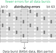
We tackle this problem and mitigate potential uncorrectable errors by leveraging awareness of design-induced variation. Our key idea is to distribute the high-error bits across different ECC codewords. We call this mechanism design-induced-variation-aware data shuffling (DIVA Shuffling).111111While it is possible that different placement algorithms for DIVA Shuffling could affect the latency and failure probability, the search space of such algorithms is very large. We choose an intuitive algorithm based on our observations of where errors and high-latency regions lie within DRAM, and find that this algorithm results in high performance with significant improvements in reliability.
There are two potential ways in which such a shuffling mechanism can be implemented. The first way is using DRAM chips that have different data-out mappings, by changing the DRAM chips internally during their manufacturing. Since the data mapping is changed internally in the DRAM chips to shuffle the high-error bits across different ECC codewords, the address decoding mechanism for reads and writes can remain identical across DRAM chips. The second way is to shuffle the address mapping of DRAM chips within a DIMM. We achieve this by connecting the address bus bits in a different order for different DRAM chips in a DIMM, thereby enabling different column addresses to be provided by different DRAM chips. Using these two mechanisms, we can achieve data shuffling in the data output from DRAM (as Figure 16b shows), which leads to fewer errors in all data bursts.
Figure 17 shows the fraction of correctable errors from a total of 72 DIMMs using SECDED ECC with and without DIVA Shuffling. We recorded the error locations and then filtered out correctable errors assuming SECDED ECC. The Y-axis represents the total percentage of errors with lower DRAM timing parameters, and the X-axis represents 33 (randomly selected) DIMMs. The operating conditions (i.e., the reduced latencies) were chosen to make sure that there are actually errors, so that ECC is useful.

Our DIVA Shuffling mechanism corrects 26% of the errors that are not correctable by using only conventional ECC. In some DIMMs, DIVA Shuffling corrects 100% of the errors, while some other DIMMs still experience errors even with DIVA Shuffling. We believe that the major cause for this is the malfunction of DRAM core operation, leading to excessively high error rates. Overall, we conclude that using DIVA Shuffling along with ECC can significantly reduce the error rate than using conventional ECC alone.
6.3. DRAM Latency & Performance Analysis
DRAM Latency Profiling. We profile 96 DIMMs, comprising 768 DRAM chips, for potential latency reduction. We use the same test methodology, described in Section 4, which is also similar to the methodology of previous works (lee-hpca2015, ; chandrasekar-date2014, ). We measure the latency reduction of four timing parameters (tRCD, tRAS, tRP, and tWR).
Figure 18 shows the average latency reduction for DRAM read and write operations with three mechanisms — AL-DRAM (lee-hpca2015, ), DIVA Profiling, and the combination of DIVA Profiling and DIVA Shuffling — normalized to the sum of the corresponding baseline timing parameters. We compare these mechanisms at two operating temperatures, 55 \oldcelsius and 85 \oldcelsius . We ignore the fact that AL-DRAM does not account for latency changes due to aging and wearout, and assume aggressive latency reductions for it, giving AL-DRAM an unfair advantage. AL-DRAM (lee-hpca2015, ) can reduce the latency for read/write operations by 33.0% (18 cycles) and 55.2% (18 cycles) at 55 \oldcelsius , and 21.3% (12 cycles) and 34.3% (19 cycles) at 85 \oldcelsius , respectively. DIVA Profiling reduces the corresponding latencies by 35.1% (22 cycles) and 57.8% (20 cycles) at 55 \oldcelsius , and 34.8% (22 cycles) and 57.5% (20 cycles) at 85 \oldcelsius , respectively. Using DIVA Shuffling on top of DIVA Profiling enables more latency reduction (by 1.8% on average). Thus, even though we give an unfair advantage to AL-DRAM in our evaluation, our mechanisms achieve better latency reduction compared to AL-DRAM, mainly because ECC (and also ECC with DIVA Shuffling) can correct single-bit errors in an ECC codeword. Specifically, increasing the temperature from 55 \oldcelsius to 85 \oldcelsius with the same set of timing parameters mostly generates single-bit and randomly distributed errors that can be corrected by ECC. Since AL-DRAM does not employ ECC, its latency benefits degrade at high temperatures, whereas our mechanism’s latency benefits remain high at all temperatures.


Performance Evaluation. We simulate the performance of our DIVA Profiling mechanism using a modified version of Ramulator (kim-cal2015, ), a fast, cycle-accurate DRAM simulator that is publicly available (ramulator, ). We use Ramulator combined with a cycle-level x86 multi-core simulator. Table 1 shows the system configuration we model. We use PinPoints (luk-pldi2005, ; patil-micro2004, ) to collect workload traces. We use 32 benchmarks from Stream (stream, ; moscibroda-usenix2007, ), SPEC CPU2006 (spec, ), TPC (tpc, ) and GUPS (gups, ), each of which is used for a single-core workload. We construct 32 two-, four-, and eight-core workloads, for a total of 96 multi-core workloads (randomly selected from the 32 benchmarks). We measure single-core performance using instructions per cycle (IPC) and multi-core performance using the weighted speedup (snavely-asplos2000, ; eyerman-ieeemicro2008, ) metric. We simulate 100 million instructions at 85 \oldcelsius for each benchmark.
| Component | Parameters |
|---|---|
| Processor | 8 cores, 3.2GHz, 3-wide issue, |
| 8 MSHRs/core, 128-entry inst. window | |
| Last-level cache | 64B cache-line, 16-way associative, |
| 512KB private cache-slice per core | |
| Mem. Controller | 64/64-entry read/write queues, FR-FCFS (rixner-isca2000, ; zuravleff-patent1997, ) |
| Memory system | DDR3-1600 (ddr3, ), 2 channels, 2 ranks-per-channel |
Figure 19 shows the performance improvement with DIVA Profiling and DIVA Shuffling. We draw two major conclusions. First, DIVA Profiling provides significant performance improvements over the baseline DRAM (9.2%/14.7%/13.7%/13.8% performance improvement in single-/two-/four-/eight-core systems, respectively). This improvement is mainly due to the reduction in DRAM latency. Second, using DIVA Profiling and DIVA Shuffling together provides even better performance improvements (by 0.5% on average) due to the additional latency reductions enabled by DIVA Shuffling.121212Note that the main reason we design DIVA Shuffling is to improve reliability (while using reduced latency parameters), not performance. Our techniques achieve these performance improvements by dynamically monitoring and optimizing DRAM latency in a reliable manner (using DIVA Profiling), while also improving DRAM reliability (using DIVA Shuffling). Third, DIVA-DRAM shows less performance sensitivity to temperature when compared to AL-DRAM (as shown in Figure 18). In general, increasing temperature leads to more randomly-distributed single-bit errors, which limits the performance benefits from AL-DRAM at high temperatures (as shown for 85 \oldcelsius in Figure 19). DIVA-DRAM incorporates ECC, and, hence, is able to correct these single-bit errors, enabling latency reductions (and performance improvement) similar to what we observe at lower temperatures.

Figure 19 also shows that our techniques outperform AL-DRAM for all four configurations by 2.5%/3.4%/3.2%/2.6%, even though we assume aggressive raw DRAM latency reductions for AL-DRAM (Section 6.3). We also ignore the fact that AL-DRAM is unable to account for dynamic latency changes due to aging and wear-out, and is thus an unrealistic mechanism (Section 6.1). Considering that aging or post-packaging failures affect a significant number of DRAM parts (sridharan-sc2012, ; sridharan-sc2013, ; meza-dsn2015, ; schroeder-tdsc2010, ; li-atc2007, ; hwang-asplos2012, ) and AL-DRAM cannot handle such failures, we conclude that our mechanisms would provide even higher performance (and reliability) improvements over AL-DRAM in reality than we have shown.
7. Related Work
To our knowledge, this is the first work to i) experimentally demonstrate and characterize design-induced latency variation across cells in real DRAM chips, ii) develop mechanisms that take advantage of this existing design-induced variation to reliably reduce DRAM latency as well as to mitigate errors, and iii) devise a practical mechanism to dynamically determine the lowest latency at which to operate DRAM reliably.
Low Latency DRAM Organizations. There are multiple proposals that aim to reduce DRAM latency by changing DRAM internals. Our proposals can be combined with these techniques to further reduce DRAM latency. Son et al. (son-isca2013, ) enable low-latency access to banks near IO pads and shorten bitlines to some subarrays, which reduces DRAM latency at the expense of additional chip area (lee-hpca2013, ; kim-isca2012, ). Our work, on the other hand, performs a comprehensive experimental analysis of design-induced variation across wordlines and bitlines at the mat level, and proposes new mechanisms to take advantage of such mat-level latency variation. Lee et al. (lee-hpca2013, ) propose TL-DRAM, a new subarray organization that enables lower access latency to cells near local sense amplifiers. To achieve this, TL-DRAM adds isolation transistors to separate a bitline into near and far segments, thereby adding a small but non-negligible area overhead to DRAM. RL-DRAM reduces DRAM latency by using smaller subarrays (rldram, ), but this comes at a significant increase in chip area. In contrast to all these works, DIVA-DRAM reduces latency and mitigates DRAM errors with no changes to the DRAM mat design. Furthermore, while prior works (lee-hpca2013, ; son-isca2013, ) are based on simulation results using a circuit-level DRAM model, we profile real DIMMs and experimentally analyze design-induced variation. Our new method of finding the slowest regions in DRAM, DIVA Profiling, is applicable to all these prior works.
Exploiting Process and Temperature Variations to Reduce DRAM Latency. Lee et al.’s AL-DRAM (lee-hpca2015, ) and Chandrasekar et al. (chandrasekar-date2014, ) lower DRAM latency by leveraging latency variation in DRAM due to the manufacturing process and temperature dependency. In contrast to our work, these two works are different in two major ways. First, they are not aware of and do not exploit design-induced latency variation in DRAM, which is due to the design and placement of components in a DRAM chip and is independent of the manufacturing process and temperature. Unlike process variation, design-induced variation, as we have experimentally shown (in Section 5), i) is dependent on the internal design of DRAM, ii) does not change over time, and iii) is similar across DRAM chips that have the same design. Second, these two works do not provide an online method for dynamically identifying the lowest latency at which to operate DRAM reliably. Instead, they assume such latencies are provided by the DRAM interface, which i) not only is difficult to achieve due to increased cost on the DRAM manufacturer’s end and the difficulty in changing the DRAM standard, ii) but also cannot adapt to increases in actual DRAM latency over time due to aging and wearout (and therefore would lead to large margin in the provided latencies). Finally, neither of these two works develop an online profiling or error correction mechanism, which our work develops. We have already provided both extensive qualitative (Section 6.1) and quantitative (Section 6.3) comparisons to AL-DRAM and shown that our mechanism significantly outperforms AL-DRAM, without requiring a priori knowledge of the lowest latency at which to operate DRAM reliably (which AL-DRAM does require), even when our simulations assume that AL-DRAM provides very aggressive latency reductions (ignoring the fact that AL-DRAM does not account for aging and wearout).
Experimental Study of DRAM Failures. Many works (kim-isca2014, ; khan-sigmetrics2014, ; lee-hpca2015, ; liu-isca2013, ; kim-edl2009, ; chandrasekar-date2014, ; chang-sigmetrics2016, ; khan-cal2016, ; chang-sigmetrics2017, ; patel-isca2017, ; khan-dsn2016, ; qureshi-dsn2015, ; kim-thesis2015, ; lee-thesis2016, ; chang-thesis2017, ) provide experimental studies and models for DRAM errors due to different type of failures such as: i) retention time failures (khan-sigmetrics2014, ; liu-isca2013, ; kim-edl2009, ; qureshi-dsn2015, ; patel-isca2017, ; khan-dsn2016, ; khan-cal2016, ), ii) wordline coupling failures (kim-isca2014, ; mutlu-date2017, ; kim-thesis2015, ), iii) failures due to lower timing parameters (lee-hpca2015, ; chandrasekar-date2014, ; chang-sigmetrics2016, ; lee-thesis2016, ; chang-thesis2017, ), and iv) failures due to reduced-voltage operation (chang-sigmetrics2017, ; chang-thesis2017, ). Specifically, Chang et al. (chang-sigmetrics2016, ) observe the non-uniform distribution of DRAM errors due to reduced latency, but do not provide the fundamental reasoning behind this non-uniformity. This work also proposes reducing DRAM latency for some cells, but does not provide a mechanism for finding the lowest DRAM latency and instead assumes that the latency of each cell is provided by the DRAM device. Our experiments and analyses focus on understanding failures due to reducing latency in design-induced vulnerable regions in DRAM, which has not been studied by any of these works. Previous failure modes, e.g., Row Hammer (kim-isca2014, ; mutlu-date2017, ; kim-thesis2015, ) or retention failures (kim-edl2009, ; liu-isca2013, ; patel-isca2017, ), do not exhibit design-induced variation, i.e., they are not dependent on cell distance from peripheral DRAM structures, as shown in prior work (kim-isca2014, ; kim-edl2009, ).
Study of DRAM Failures in Large Scale Systems. Many previous works (sridharan-sc2012, ; sridharan-sc2013, ; meza-dsn2015, ; schroeder-tdsc2010, ; li-atc2007, ; hwang-asplos2012, ; schroeder-sigmetrics2009, ) study DRAM errors in large scale systems (e.g., a server cluster or many data centers) and analyze the system-level impact on DRAM failures, e.g., power fluctuation, operating temperature, wearout, etc. Our analyses are orthogonal to these studies and focus on the impact of internal DRAM organization on latency and error characteristics.
DRAM Error Mitigation Techniques. To increase system reliability and efficiency, many error correction codes (alameldeen-isca2011, ; kim-hpca2015, ; wilkerson-isca2010, ; luo-dsn2014, ) have been proposed specifically in the context of DRAM error mitigation (khan-sigmetrics2014, ). VS-ECC (alameldeen-isca2011, ) proposes variable strength error correction codes for better performance and energy efficiency. HI-ECC (wilkerson-isca2010, ) increases power efficiency for high-capacity eDRAM-based caches by integrating a strong error correction code.
Our proposals complement existing ECC mechanisms and achieve better performance and reliability. First, having ECC alone (regardless of ECC strength) is not enough to guarantee correct operation with maximum latency reduction, since it is not possible to determine the smallest value for each timing parameter without profiling. DIVA Profiling can do so, enabling maximum latency reduction while leveraging ECC support to correct failures. Second, DIVA Shuffling enables greater reliability in the presence of an ECC mechanism by distributing possible errors over different ECC codewords. Third, our work opens up new research opportunities to exploit design-induced variation in combination with different ECC schemes. For example, variable-strength ECC (alameldeen-isca2011, ) can exploit awareness of design-induced variation by adjusting ECC strength based on error probability indications/predictions from design-induced variation.
DRAM Latency Reduction with In-Memory Communication and Computation. Transferring data over the memory channel leads to long latency and delays other data transfers. To reduce this latency, prior works offload bulk data movement (seshadri-micro2013, ; chang-hpca2016, ; lee-pact2015, ) or computation operations (e.g., (seshadri-cal2015, ; ahn-isca2015a, ; ahn-isca2015b, ; patterson-ieeemicro1997, ; mirzadeh-asbd2015, ; kogge-icpp1994, ; kocberber-micor2013, ; guo-wondp2014, ; gao-pact2015, ; farahani-hpca2015, ; boroumand-cal2016, ; hsieh-isca2016, ; seshadri-arxiv2016, ; stone-tc1970, ; seshadri-micro2015, ; hsieh-iccd2016, ; pattnaik-pact2016, )) to DRAM. These works do not fundamentally reduce the access latency to the DRAM array, whereas our proposal DIVA-DRAM does. Hence, DIVA-DRAM is complementary to such in-memory communication and computation mechanisms.
DRAM Latency Reduction Based on Memory Access Patterns. Prior works (shin-hpca2014, ; hassan-hpca2016, ) show that DRAM leakage affects two DRAM timing parameters (tRCD/tRAS), and recently-accessed rows have more charge. This allows such rows to be reliably accessed with a lower latency than the DRAM standard. Our approach of reducing latency by taking advantage of design-induced variation is complementary to these works.
8. Conclusion
This paper provides the first study that experimentally characterizes and exploits the phenomenon of design-induced variation in real DRAM chips. Based on a detailed experimental analysis of 768 modern DRAM chips from three major manufacturers, we find that there is widespread variation in the access latency required for reliable operation of DRAM cells, depending on how close or far the cells are to the peripheral structures that are used to access them. We introduce DIVA-DRAM, which consists of two novel techniques that take advantage of design-induced variation to i) reduce DRAM latency reliably at low cost and ii) improve reliability by making ECC more effective. DIVA Profiling reduces DRAM latency by finding the lowest latency at which to operate DRAM reliably, by dynamically profiling certain cells that are most vulnerable to failures caused by reduced-latency operation, due to the design of the DRAM chip. DIVA Shuffling improves DRAM reliability by intelligently shuffling data such that errors induced due to reduced-latency operation become correctable by ECC. Our comprehensive experimental evaluations demonstrate that DIVA-DRAM can greatly reduce DRAM read/write latency, leading to significant system performance improvements on a variety of workloads and system configurations, compared to both modern DRAM and the state-of-the-art Adaptive-Latency DRAM (lee-hpca2015, ). We conclude that exploiting the design-induced latency variation inherent in DRAM using our new techniques provides a promising, reliable, and low-cost way of significantly reducing DRAM latency. We hope that our comprehensive experimental characterization and analysis of design-induced variation in modern DRAM chips enables the development of other mechanisms to improve DRAM latency and reliability.
ACKNOWLEDGMENTS
We thank the reviewers of SIGMETRICS 2017, HPCA 2017, MICRO 2016, HPCA 2016, and ISCA 2016 for their comments. We especially thank the reviewers of SIGMETRICS 2017 for their constructive and insightful comments. An earlier version of this work was posted on arXiv (lee-arxiv2016, ). We acknowledge the generous support of Google, Intel, NVIDIA, Samsung, and VMware. This work is supported in part by NSF grants 1212962, 1320531, and 1409723, the Intel Science and Technology Center for Cloud Computing, and the Semiconductor Research Corporation.
References
- [1] DIVA-DRAM Simulation Model and Experimental Data. https://github.com/CMU-SAFARI/DIVA-DRAM.
- [2] Ramulator. https://github.com/CMU-SAFARI/ramulator.
- [3] J. Ahn, S. Hong, S. Yoo, O. Mutlu, and K. Choi. A Scalable Processing-in-Memory Accelerator for Parallel Graph Processing. In ISCA, 2015.
- [4] J. Ahn, S. Yoo, O. Mutlu, and K. Choi. PIM-Enabled Instructions: A Low-Overhead, Locality-Aware Processing-in-Memory Architecture. In ISCA, 2015.
- [5] A. Ailamaki, D. J. DeWitt, M. D. Hill, and D. A. Wood. DBMSs on a Modern Processor: Where Does Time Go? In VLDB, 1999.
- [6] A. R. Alameldeen, I. Wagner, Z. Chishti, W. Wu, C. Wilkerson, and S.-L. Lu. Energy-Efficient Cache Design Using Variable-Strength Error-Correcting Codes. In ISCA, 2011.
- [7] Arizona State Univ. Predictive Technology Model. http://ptm.asu.edu/, 2012.
- [8] K. Arndt, C. Narayan, A. Brintzinger, W. Guthrie, D. Lachtrupp, J. Mauger, D. Glimmer, S. Lawn, B. Dinkel, and A. Mitwalsky. Reliability of Laser Activated Metal Fuses in DRAMs. In IEMT, 1999.
- [9] S. Borkar and A. A. Chien. The Future of Microprocessors. In CACM, 2011.
- [10] A. Boroumand, S. Ghose, B. Lucia, K. Hsieh, K. Malladi, H. Zheng, and O. Mutlu. LazyPIM: An Efficient Cache Coherence Mechanism for Processing-in-Memory. In IEEE CAL, 2016.
- [11] S. Cha, S. O, H. Shin, S. Hwang, K. Park, S. Jang, J. Choi, G. Jin, Y. Son, H. Cho, J. Ahn, and N. Kim. Defect Analysis and Cost Effective Resilience Architecture for Future DRAM Devices. In HPCA, 2017.
- [12] K. Chandrasekar, S. Goossens, C. Weis, M. Koedam, B. Akesson, N. Wehn, and K. Goossens. Exploiting Expendable Process-Margins in DRAMs for Run-Time Performance Optimization. In DATE, 2014.
- [13] K. K. Chang. Understanding and Improving Latency of DRAM-Based Memory Systems. PhD thesis, Carnegie Mellon University, 2017.
- [14] K. K. Chang, A. Kashyap, H. Hassan, S. Ghose, K. Hsieh, D. Lee, T. Li, G. Pekhimenko, S. Khan, and O. Mutlu. Understanding Latency Variation in Modern DRAM Chips: Experimental Characterization, Analysis, and Optimization. In SIGMETRICS, 2016.
- [15] K. K. Chang, D. Lee, Z. Chishti, A. Alameldeen, C. Wilkerson, Y. Kim, and O. Mutlu. Improving DRAM Performance by Parallelizing Refreshes with Accesses. In HPCA, 2014.
- [16] K. K. Chang, P. J. Nair, S. Ghose, D. Lee, M. K. Qureshi, and O. Mutlu. Low-Cost Inter-Linked Subarrays (LISA): Enabling Fast Inter-Subarray Data Movement in DRAM. In HPCA, 2016.
- [17] K. K. Chang, A. G. Yaglikci, A. Agrawal, N. Chatterjee, S. Ghose, A. Kashyap, H. Hassan, D. Lee, M. O’Connor, and O. Mutlu. Understanding Reduced-Voltage Operation in Modern DRAM Devices: Experimental Characterization, Analysis, and Mechanisms. In SIGMETRICS, 2017.
- [18] C. Elm, M. Klein, and D. Tavangarian. Automatic On-Line Memory Tests in Workstations. In MTDT, 1994.
- [19] S. Eyerman and L. Eeckhout. System-Level Performance Metrics for Multiprogram Workloads. In IEEE Micro, 2008.
- [20] A. Farmahini-Farahani, J. H. Ahn, K. Morrow, and N. S. Kim. NDA: Near-DRAM Acceleration Architecture Leveraging Commodity DRAM Devices and Standard Memory Modules. In HPCA, 2015.
- [21] M. Gao, G. Ayers, and C. Kozyrakis. Practical Near-Data Processing for In-Memory Analytics Frameworks. In PACT, 2015.
- [22] Q. Guo, N. Alachiotis, B. Akin, F. Sadi, G. Xu, T. M. Low, L. Pileggi, J. C. Hoe, and F. Franchetti. 3D-Stacked Memory-Side Acceleration: Accelerator and System Design. In WoNDP, 2014.
- [23] H. Hassan, G. Pekhimenko, N. Vijaykumar, V. Seshadri, D. Lee, O. Ergin, and O. Mutlu. ChargeCache: Reducing DRAM Latency by Exploiting Row Access Locality. In HPCA, 2016.
- [24] H. Hassan, N. Vijaykumar, S. Khan, S. Ghose, K. Chang, G. Pekhimenko, D. Lee, O. Ergin, and O. Mutlu. SoftMC: A Flexible and Practical Open-Source Infrastructure for Enabling Experimental DRAM Studies. In HPCA, 2017.
- [25] M. Horiguchi and K. Itoh. Nanoscale Memory Repair. Springer, 2013.
- [26] HPC Challenge. GUPS. http://icl.cs.utk.edu/projectsfiles/hpcc/RandomAccess/.
- [27] K. Hsieh, E. Ebrahimi, G. Kim, N. Chatterjee, M. O’Connor, N. Vijaykumar, O. Mutlu, and S. W. Keckler. Transparent Offloading and Mapping (TOM): Enabling Programmer-Transparent Near-Data Processing in GPU Systems. In ISCA, 2016.
- [28] K. Hsieh, S. Khan, N. Vijaykumar, K. K. Chang, A. Boroumand, S. Ghose, and O. Mutlu. Accelerating Pointer Chasing in 3D-Stacked Memory: Challenges, Mechanisms, Evaluation. In ICCD, 2016.
- [29] A. A. Hwang, I. A. Stefanovici, and B. Schroeder. Cosmic Rays Don’t Strike Twice: Understanding the Nature of DRAM Errors and the Implications for System Design. In ASPLOS, 2012.
- [30] M. Inoue, T. Yamada, H. Kotani, H. Yamauchi, A. Fujiwara, J. Matsushima, H. Akamatsu, M. Fukumoto, M. Kubota, I. Nakao, N. Aoi, G. Fuse, S. Ogawa, S. Odanaka, A. Ueno, and H. Yamamoto. A 16-Mbit DRAM with a Relaxed Sense-Amplifier-Pitch Open-Bit-Line Architecture. In JSSC, 1988.
- [31] JEDEC Solid State Technology Assn. JESD79-3F: DDR3 SDRAM Standard, 2012.
- [32] T. S. Jung. Memory technology and solutions roadmap. http://www.sec.co.kr/images/corp/ir/irevent/techforum_01.pdf, 2005.
- [33] U. Kang, H.-S. Yu, C. Park, H. Zheng, J. Halbert, K. Bains, S. Jang, and J. Choi. Co-Architecting Controllers and DRAM to Enhance DRAM Process Scaling. In The Memory Forum, 2014.
- [34] B. Keeth, R. J. Baker, B. Johnson, and F. Lin. DRAM Circuit Design: Fundamental and High-Speed Topics. Wiley-IEEE Press, 2007.
- [35] S. Khan, D. Lee, Y. Kim, A. R. Alameldeen, C. Wilkerson, and O. Mutlu. The Efficacy of Error Mitigation Techniques for DRAM Retention Failures: A Comparative Experimental Study. In SIGMETRICS, 2014.
- [36] S. Khan, D. Lee, and O. Mutlu. PARBOR: An Efficient System-Level Technique to Detect Data-Dependent Failures in DRAM. In DSN, 2016.
- [37] S. Khan, C. Wilkerson, D. Lee, A. R. Alameldeen, and O. Mutlu. A Case for Memory Content-Based Detection and Mitigation of Data-Dependent Failures in DRAM. In IEEE CAL, 2016.
- [38] J. Kim, M. Sullivan, and M. Erez. Bamboo ECC: Strong, Safe, and Flexible Codes for Reliable Computer Memory. In HPCA, 2015.
- [39] K. Kim and J. Lee. A New Investigation of Data Retention Time in Truly Nanoscaled DRAMs. In EDL, 2009.
- [40] Y. Kim. Architectural Techniques to Enhance DRAM Scaling. PhD thesis, Carnegie Mellon University, 2015.
- [41] Y. Kim, R. Daly, J. Kim, C. Fallin, J. H. Lee, D. Lee, C. Wilkerson, K. Lai, and O. Mutlu. Flipping Bits in Memory Without Accessing Them: An Experimental Study of DRAM Disturbance Errors. In ISCA, 2014.
- [42] Y. Kim, V. Seshadri, D. Lee, J. Liu, and O. Mutlu. A Case for Exploiting Subarray-Level Parallelism (SALP) in DRAM. In ISCA, 2012.
- [43] Y. Kim, W. Yang, and O. Mutlu. Ramulator: A Fast and Extensible DRAM Simulator. In IEEE CAL, 2015.
- [44] O. Kocberber, B. Grot, J. Picorel, B. Falsafi, K. Lim, and P. Ranganathan. Meet the Walkers: Accelerating Index Traversals for In-Memory Databases. In MICRO, 2013.
- [45] P. M. Kogge. EXECUBE-A New Architecture for Scaleable MPPs. In ICPP, 1994.
- [46] D. Lee. Reducing DRAM Latency at Low Cost by Exploiting Heterogeneity. PhD thesis, Carnegie Mellon University, 2016.
- [47] D. Lee, S. M. Khan, L. Subramanian, R. Ausavarungnirun, G. Pekhimenko, V. Seshadri, S. Ghose, and O. Mutlu. Reducing DRAM Latency by Exploiting Design-Induced Latency Variation in Modern DRAM Chips. In CoRR abs/1610.09604, 2016.
- [48] D. Lee, Y. Kim, G. Pekhimenko, S. Khan, V. Seshadri, K. Chang, and O. Mutlu. Adaptive-Latency DRAM: Optimizing DRAM Timing for the Common-Case. In HPCA, 2015.
- [49] D. Lee, Y. Kim, V. Seshadri, J. Liu, L. Subramanian, and O. Mutlu. Tiered-Latency DRAM: A Low Latency and Low Cost DRAM Architecture. In HPCA, 2013.
- [50] D. Lee, L. Subramanian, R. Ausavarungnirun, J. Choi, and O. Mutlu. Decoupled Direct Memory Access: Isolating CPU and IO Traffic by Leveraging a Dual-Data-Port DRAM. In PACT, 2015.
- [51] X. Li, K. Shen, M. C. Huang, and L. Chu. A Memory Soft Error Measurement on Production Systems. In USENIX ATC, 2007.
- [52] J. Liu, B. Jaiyen, Y. Kim, C. Wilkerson, and O. Mutlu. An Experimental Study of Data Retention Behavior in Modern DRAM Devices: Implications for Retention Time Profiling Mechanisms. In ISCA, 2013.
- [53] J. Liu, B. Jaiyen, R. Veras, and O. Mutlu. RAIDR: Retention-Aware Intelligent DRAM Refresh. In ISCA, 2012.
- [54] C.-K. Luk, R. Cohn, R. Muth, H. Patil, A. Klauser, G. Lowney, S. Wallace, V. J. Reddi, and K. Hazelwood. Pin: Building Customized Program Analysis Tools with Dynamic Instrumentation. In PLDI, 2005.
- [55] Y. Luo, S. Govindan, B. Sharma, M. Santaniello, J. Meza, A. Kansal, J. Liu, B. Khessib, K. Vaid, and O. Mutlu. Characterizing Application Memory Error Vulnerability to Optimize Datacenter Cost via Heterogeneous-Reliability Memory. In DSN, 2014.
- [56] J. D. McCalpin. STREAM Benchmark. http://www.streambench.org/.
- [57] J. Meza, Q. Wu, S. Kumar, and O. Mutlu. Revisiting Memory Errors in Large-Scale Production Data Centers: Analysis and Modeling of New Trends from the Field. In DSN, 2015.
- [58] Micron Technology, Inc. RLDRAM 2 and 3 Specifications. http://www.micron.com/products/dram/rldram-memory.
- [59] Micron Technology, Inc. 4Gb DDR3 SDRAM (MT41J512M8), 2012.
- [60] K.-S. Min, J.-T. Park, S.-P. Lee, Y.-H. Kim, T.-H. Yang, J.-D. Joo, K.-M. Lee, J.-K. Wee, and J.-Y. Chung. A Post-Package Bit-Repair Scheme Using Static Latches with Bipolar-Voltage Programmable Antifuse Circuit for High-Density DRAMs. In VLSI, 2001.
- [61] N. S. Mirzadeh, O. Kocberber, B. Falsafi, and B. Grot. Sort vs. Hash Join Revisited for Near-Memory Execution. In ASBD, 2015.
- [62] Y. Mori, K. Ohyu, K. Okonogi, and R.-I. Yamada. The Origin of Variable Retention Time in DRAM. In IEDM, 2005.
- [63] T. Moscibroda and O. Mutlu. Memory Performance Attacks: Denial of Memory Service in Multi-Core Systems. In USENIX Security, 2007.
- [64] O. Mutlu. Memory Scaling: A Systems Architecture Perspective. In IMW, 2013.
- [65] O. Mutlu. The RowHammer Problem and Other Issues We May Face as Memory Becomes Denser. In DATE, 2017.
- [66] O. Mutlu, J. Stark, C. Wilkerson, and Y. N. Patt. Runahead Execution: An Alternative to Very Large Instruction Windows for Out-of-Order Processors. In HPCA, 2003.
- [67] O. Mutlu and L. Subramanian. Research Problems and Opportunities in Memory Systems. In SUPERFRI, 2014.
- [68] P. J. Nair, D.-H. Kim, and M. K. Qureshi. ArchShield: Architectural Framework for Assisting DRAM Scaling by Tolerating High Error Rates. In ISCA, 2013.
- [69] M. Patel, J. Kim, and O. Mutlu. The Reach Profiler (REAPER): Enabling the Mitigation of DRAM Retention Failures via Profiling at Aggressive Conditions. In ISCA, 2017.
- [70] H. Patil, R. Cohn, M. Charney, R. Kapoor, A. Sun, and A. Karunanidhi. Pinpointing Representative Portions of Large Intel Itanium Programs with Dynamic Instrumentation. In MICRO, 2004.
- [71] D. Patterson, T. Anderson, N. Cardwell, R. Fromm, K. Keeton, C. Kozyrakis, R. Thomas, and K. Yelick. A Case for Intelligent RAM. In IEEE Micro, 1997.
- [72] D. A. Patterson. Latency Lags Bandwidth. In CACM, 2004.
- [73] A. Pattnaik, X. Tang, A. Jog, O. Kayiran, A. K. Mishra, M. T. Kandemir, O. Mutlu, and C. R. Das. Scheduling Techniques for GPU Architectures with Processing-in-Memory Capabilities. In PACT, 2016.
- [74] M. Qureshi, D.-H. Kim, S. Khan, P. Nair, and O. Mutlu. AVATAR: A Variable-Retention-Time (VRT) Aware Refresh for DRAM Systems. In DSN, 2015.
- [75] M. Rahman, B. Childers, and S. Cho. COMeT: Continuous Online Memory Test. In PRDC, 2011.
- [76] P. J. Restle, J. W. Park, and B. F. Lloyd. DRAM Variable Retention Time. In IEDM, 1992.
- [77] S. Rixner, W. J. Dally, U. J. Kapasi, P. Mattson, and J. D. Owens. Memory Access Scheduling. In ISCA, 2000.
- [78] B. Schroeder and G. Gibson. A Large-Scale Study of Failures in High-Performance Computing Systems. In TDSC, 2010.
- [79] B. Schroeder, E. Pinheiro, and W.-D. Weber. DRAM Errors in the Wild: A Large-Scale Field Study. In SIGMETRICS, 2009.
- [80] V. Seshadri, K. Hsieh, A. Boroumand, D. Lee, M. Kozuch, O. Mutlu, P. Gibbons, and T. Mowry. Fast Bulk Bitwise AND and OR in DRAM. In IEEE CAL, 2015.
- [81] V. Seshadri, Y. Kim, C. Fallin, D. Lee, R. Ausavarungnirun, G. Pekhimenko, Y. Luo, O. Mutlu, P. B. Gibbons, M. A. Kozuch, and T. C. Mowry. RowClone: Fast and Energy-Efficient In-DRAM Bulk Data Copy and Initialization. In MICRO, 2013.
- [82] V. Seshadri, D. Lee, T. Mullins, H. Hassan, A. Boroumand, J. Kim, M. A. Kozuch, O. Mutlu, P. B. Gibbons, and T. C. Mowry. Buddy-RAM: Improving the Performance and Efficiency of Bulk Bitwise Operations Using DRAM. In CoRR abs/1605.06483, 2016.
- [83] V. Seshadri, T. Mullins, A. Boroumand, O. Mutlu, P. B. Gibbons, M. A. Kozuch, and T. C. Mowry. Gather-Scatter DRAM: In-DRAM Address Translation to Improve the Spatial Locality of Non-Unit Strided Accesses. In MICRO, 2015.
- [84] W. Shin, J. Yang, J. Choi, and L.-S. Kim. NUAT: A Non-Uniform Access Time Memory Controller. In HPCA, 2014.
- [85] A. Singh, D. Bose, and S. Darisala. Software Based In-System Memory Test for Highly Available Systems. In MTDT, 2005.
- [86] A. Snavely and D. M. Tullsen. Symbiotic Jobscheduling for a Simultaneous Multithreaded Processor. In ASPLOS, 2000.
- [87] Y. H. Son, O. Seongil, Y. Ro, J. W. Lee, and J. H. Ahn. Reducing Memory Access Latency with Asymmetric DRAM Bank Organizations. In ISCA, 2013.
- [88] V. Sridharan and D. Liberty. A Study of DRAM Failures in the Field. In SC, 2012.
- [89] V. Sridharan, J. Stearley, N. DeBardeleben, S. Blanchard, and S. Gurumurthi. Feng Shui of Supercomputer Memory: Positional Effects in DRAM and SRAM Faults. In SC, 2013.
- [90] Standard Performance Evaluation Corp. SPEC CPU2006. http://www.spec.org/cpu2006.
- [91] H. S. Stone. A Logic-in-Memory Computer. In IEEE TC, 1970.
- [92] A. Tanabe, T. Takeshima, H. Koike, Y. Aimoto, M. Takada, T. Ishijima, N. Kasai, H. Hada, K. Shibahara, T. Kunio, T. Tanigawa, T. Saeki, M. Sakao, H. Miyamoto, H. Nozue, S. Ohya, T. Murotani, K. Koyama, and T. Okuda. A 30-ns 64-Mb DRAM with Built-In Self-Test and Self-Repair Function. In JSSC, 1992.
- [93] Transaction Processing Performance Council. TPC Benchmark. http://www.tpc.org/.
- [94] A. J. van de Goor and I. Schanstra. Address and Data Scrambling: Causes and Impact on Memory Tests. In DELTA, 2002.
- [95] R. Venkatesan, S. Herr, and E. Rotenberg. Retention-Aware Placement in DRAM (RAPID): Software Methods for Quasi-Non-Volatile DRAM. HPCA, 2006.
- [96] T. Vogelsang. Understanding the Energy Consumption of Dynamic Random Access Memories. In MICRO, 2010.
- [97] J.-K. Wee, W. Yang, E.-K. Ryou, J.-S. Choi, S.-H. Ahn, J.-Y. Chung, and S.-C. Kim. An Antifuse EPROM Circuitry Scheme for Field-Programmable Repair in DRAM. In JSSC, 2000.
- [98] C. Wilkerson, A. R. Alameldeen, Z. Chishti, W. Wu, D. Somasekhar, and S.-L. Lu. Reducing Cache Power with Low-Cost, Multi-Bit Error-Correcting Codes. In ISCA, 2010.
- [99] Xilinx, Inc. Virtex-6 FPGA Integrated Block for PCI Express, 2011. http://www.xilinx.com/support/documentation/ip_documentation/mig/v3_92/ug406.pdf.
- [100] Xilinx, Inc. ML605 Hardware User Guide, 2012. http://www.xilinx.com/support/documentation/boards_and_kits/ug534.pdf.
- [101] Xilinx, Inc. Virtex-6 FPGA Memory Interface Solutions, 2013. http://www.xilinx.com/support/documentation/ip_documentation/mig/v3_92/ug406.pdf.
- [102] D. Yaney, C. Y. Lu, R. Kohler, M. J. Kelly, and J. Nelson. A Meta-Stable Leakage Phenomenon in DRAM Charge Storage - Variable Hold Time. In IEDM, 1987.
- [103] W. Zhao and Y. Cao. New Generation of Predictive Technology Model for Sub-45nm Design Exploration. In ISQED, 2006.
- [104] W. K. Zuravleff and T. Robinson. Controller for a Synchronous DRAM That Maximizes Throughput by Allowing Memory Requests and Commands to Be Issued Out of Order. U.S. Patent No. 5630096, 1997.
Appendix
Appendix A Latency Overhead of DIVA Profiling
In Section 6.1, we calculate the time it takes to perform both DIVA Profiling and conventional DRAM profiling (where each DRAM row is tested) [68, 53, 95, 35].
DRAM profiling consists of two steps: i) writing data to the cells that are being tested, and ii) reading and verifying cell contents. Therefore, the profiling time is calculated as:
| (1) |
where we determine the fastest rate at which a column command can be performed, and then multiply it by the number of patterns that are being tested, and by two because we perform a read and a write (i.e., two column commands) to each DRAM column.
When testing a 4GB DDR3-1600 DIMM (whose DIMM bandwidth is 1600 Mbps/pin 64 pins 102.4 Gbps) with one test pattern, conventional DRAM profiling mechanisms take 625 ms to test all 4GB of DRAM cells. However, since DIVA Profiling needs to test only 8MB of cells (i.e., just one row per each 512-row subarray), it takes only 1.22 ms to complete its test.
Appendix B DRAM Simulation to Validate Our Hypotheses on Design-Induced Variation
We hypothesize that accessing a cell that is physically farther from the structures that are required to perform the access (e.g., the sense amplifiers, the wordline drivers) takes a longer time than accessing a cell that is closer to them. Our observations in Section 5 support this hypothesis empirically, but they do not provide absolute proof because they are based on observations on DRAM chips whose internal circuitry is not publicly provided and thus is unknown to us. To verify our hypothesis, we simulate the effects of the distance between a cell and the structures required to perform the access in a DRAM mat by using a detailed SPICE circuit model. Our SPICE simulation model and parameters are publicly available [1].
Detailed Mat Model. We first build a DRAM mat model with a detailed wire model, as shown in Figure 20. Our mat model consists of a 512 x 512 array of DRAM cells, which is commonly used in modern DRAM chips [96]. Each 512-cell column is connected to a sense amplifier over a bitline, which is plotted as the vertical gray block in Figure 20. Each bitline has its own parasitic resistance and capacitance. We expect that due to the bitline’s parasitic resistance and capacitance, accessing a cell farther from a sense amplifier (e.g., cell ❷) takes a longer time than accessing a cell that is closer to the same sense amplifier (e.g., cell ❶). Each 512-cell row is connected to a local wordline driver over a wordline (512 local wordline drivers in total), which is plotted as the horizontal gray block in Figure 20. Each wordline has its own parasitic resistance and capacitance. We expect that due to the wordline’s parasitic resistance and capacitance, accessing a cell farther from a wordline driver (e.g., cell ❸) takes a longer time than accessing a cell that is closer to the same wordline driver (e.g., cell ❷).
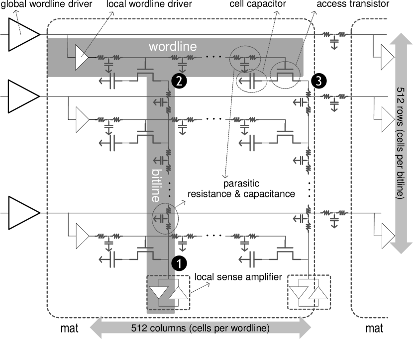
Simulation Methodology. To simulate the access latency for cells in different locations, we use technology parameters from a 55 nm DRAM model [96] and from a 45 nm logic process model [7, 103] to construct a detailed circuit-level SPICE simulation model. We assume that the cell capacitance is 24 fF, and the bitline capacitance is 144 fF [96]. The cell and sense amplifier operating voltage is 1.2V, while the wordline operating voltage is 3.0V. In our evaluation, we issue the ACTIVATION command at 0 ns and PRECHARGE at 30 ns, which replicates the behavior of using a reduced tRAS timing parameter (the standard tRAS is 35 ns [31]). We plot the circuit-level SPICE simulation results in Figure 21. Figure 21a shows the variation on voltage levels of the bitlines for two different cells: i) a cell that is near the sense amplifier (cell ❶ in Figure 20), and ii) a cell that is far from the sense amplifier (cell ❷ in Figure 20). Similarly, Figure 21b shows the variation on voltage levels of the bitline for two different cells: i) a cell that is near the wordline driver (cell ❷ in Figure 20), and ii) a cell that is far from the wordline driver (cell ❸ in Figure 20). We explain the figures and our results in detail below, but the key conclusion is that the voltage level of the cell that is closer to the sense amplifier (cell ❶) becomes higher (and lower) more quickly than that of the cell that is farther from the sense amplifier (cell ❷), as shown in Figure 21a. The same observation is true for the cell that is closer to the wordline driver (cell ❷) vs. the cell that is farther from the wordline driver (cell ❸). Since the voltage level of a cell that is closer to the sense amplifier or the wordline driver becomes higher (or lower) more quickly, that cell can be accessed faster. We explain this phenomenon in more detail below.
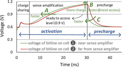
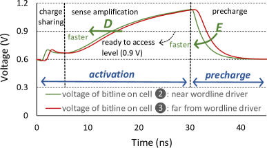
DRAM Row and Column Access. There are three steps performed to access data in a DRAM cell. The first step is selecting a wordline. Inside DRAM, there are i) a global wordline (that stretches over the entire subarray) and ii) multiple local wordlines (each of which stretches over a single mat). Enabling a global wordline driver raises the voltage of the global wordline. Then, the global wordline enables multiple local wordlines. Each wordline turns on 512 access transistors, connecting one cell capacitor in each column to its corresponding bitline. We call this step charge sharing in Figure 21. Figures 21a and 21b show that charge sharing becomes enabled by raising a wordline between 0 ns and 5 ns. In this example, the bitline voltage level (which is initially precharged to 0.6V, ) increases due to the sharing of charge from the connected cell (which we assume is initially fully charged to 1.2V, ).
Second, after charge sharing, the sense amplifiers are enabled, starting to detect the voltage perturbation caused by the charge sharing operation and amplifying the bitline voltage level toward 1.2V (). We call this step sense amplification in Figure 21. Figure 21 shows sense amplification taking place between 5 ns to 30 ns. During sense amplification, a sense amplifier can reliably transfer the detected data to the IO circuitry when the voltage level reaches 0.9V (half way between and ). In other words, the data becomes ready to access at the bitline voltage level of 0.9V.
Third, after finishing sense amplification, in order to prepare the subarray for an access to another row, the bitline voltage should be reduced to 0.6V (the initial voltage level of the bitline, ), to allow access to cells in a different row. We call this step precharge in Figure 21. Figures 21a and 21b show the precharge of a bitline taking place between 30 ns to 40 ns.
For these three steps, we can understand the latency of each step by examining the bitline voltage level. The access latencies of these operations are determined based on how quickly the bitline voltage level changes. For example, the latency of activation depends on how fast the bitline level can reach . Similarly, the latency of the precharge operation depends on how fast the bitline level can return to . In the next two paragraphs, we observe the latency of accessing cells in different locations in a mat (cells ❶, ❷, and ❸), as shown in Figures 20 and 21.
Accessing Cells on the Same Bitline. We evaluate and compare two cases for accessing cells on the same bitline: i) a cell that is near a sense amplifier (labeled cell ❶), and ii) a cell that is far from the sense amplifier (labeled cell ❷). Note that we use the same labels to describe the same cells in Figures 20 and 21. Figure 21a shows the voltage levels of the bitline when measured near the accessed cells (cells ❶ and ❷). We make three major observations. First, the cell that is near the sense amplifier (cell ❶) finishes sense amplification earlier than the cell that is far from the sense amplifier (cell ❷), as pointed to by label in Figure 21a. This is mainly due to the additional parasitic resistance and capacitance required for accessing cell ❷, which causes its voltage level to rise more slowly. Second, the restored voltage level of a cell (i.e., the highest voltage level of a bitline in Figure 21a) that is near the sense amplifier (cell ❶) is higher than the level of the cell that is far from the sense amplifier (cell ❷), as pointed to by label in Figure 21a. Therefore, when reducing the restoration time (tRAS), the cell that is far from the sense amplifier (cell ❷) holds less charge than the cell that is near the sense amplifier (cell ❶). Due to the smaller amount of charge in the far cell, accessing the far cell takes a longer time than accessing the near cell. Third, precharging the bitline when accessing the near cell takes less time than when accessing the far cell, as shown by the voltage level of cell ❶ dropping much faster than that of cell ❷ during the precharge operation (pointed to by label in Figure 21a). Therefore, reducing the precharge timing parameter (tRP) might be fine for the near cell (as the bitline can still return to full within the reduced tRP). However, for the far cell, reducing the precharge timing parameter can result in the bitline not fully returning to after we access the far cell. If the next access is to a cell whose charge state (i.e., charged/discharged) is different from the cell we just accessed, it will take longer for the next access to be ready, as the bitline voltage needs to change by a greater amount. From these detailed circuit-level evaluations, we conclude that accessing a cell that is far from the sense amplifier takes a longer time than accessing a cell that is near the sense amplifier.
Accessing Cells on the Same Local Wordline. We evaluate and compare two cases for accessing cells on the same wordline in Figures 20 and 21: i) a cell that is near a local wordline driver (labeled cell ❷), and ii) a cell that is far from the local wordline driver (labeled cell ❸). Figure 21b shows the voltage levels of the corresponding bitlines of the two cells when measured near the accessed cells. The key observation from the figure is that accessing a cell that is far from the local wordline driver takes a longer time than accessing a cell that is near the local wordline driver. This is mainly because the wordline has a large resistance and capacitance and, thus it takes longer for the activation signal to reach the far cell. As a result, the voltage level of the nearby cell becomes higher than that of the far cell, after an activation operation, as pointed to by label in Figure 21b. Also, precharging is faster for the nearby cell because its voltage level gets closer to (0.6 V) much faster than that of the far cell, as pointed to by label in Figure 21b. Similarly, other control signals (e.g., sense amplifier enable, equalizer enable) also experience wire propagation delay that is higher when accessing the far cell. As a result, the operations that take place when accessing a cell farther away from the wordline driver require a longer time to complete.
In summary, in our detailed circuit-level simulations, we observe that accessing a cell that is farther from the structures that are required to perform the access (e.g., the sense amplifiers and the wordline drivers) takes a longer time than accessing a cell that is closer to such structures. Based on these evaluations, we conclude that cells in a DRAM mat have different latency characteristics based on their location, which leads to a major source of design-induced variation.
Appendix C Design-Induced Variation vs. Process Variation
We observe two types of errors: i) errors caused by process variation that is usually randomly distributed over the entire DRAM chip [35, 11], and ii) errors caused by design-induced variation that are concentrated in specific regions (as we showed in Section 6.1). There are cases where the effect of design-induced variation on latency is greater than that of process variation, and there are cases where the effect of process variation is greater. Our mechanism, DIVA-DRAM, enables reliable operation in both cases. The total DRAM latency variation is the sum of design-induced variation and process variation. We provide a separate mechanism to reliably handle each type of variation: i) online DIVA Profiling to minimize latency by exploiting design-induced variation, and ii) ECC, strengthened with DIVA Shuffling, to provide high reliability in the presence of process variation. Because we provide ECC with improved reliability to account for the presence of process variation, we are able to safely harness the performance improvements offered by our exploitation of design-induced variation, even when the effect of process variation is higher.
We note that even in situations where process variation changes from DIMM to DIMM, one can still exploit design-induced variation for better performance and reliability by embedding the DIMM-specific information (i.e., the addresses of the slowest regions that can be used for the latency test regions in DIVA Profiling, the external-to-internal address mapping information) within the DRAM module (e.g., inside the serial-presence-detect EEPROM in a DRAM module, as described in [42]), and providing this information to the memory controller.
Appendix D List of Tested DIMMs
We report a short summary of the properties and design-induced vulnerability of each of the 96 DIMMs (from three major DRAM vendors) presented in this paper, separated by vendor, in Tables D, D, and D. The evaluated DIMMs are manufactured in the period from 2010 to 2013. While newer DIMMs enable higher capacity and bandwidth, the DRAM cell array architecture of these newer DIMMs has not changed significantly from the architecture of the DIMMs we evaluate [34]. Therefore, we believe that our observations on DRAM latency variation hold true for more recently manufactured DRAM chips.
| Vendor | Module | Date∗ | Timing† | Organization | Chip | Vulnerability Ratio⋆ | |||||
|---|---|---|---|---|---|---|---|---|---|---|---|
| (yy-ww) | Freq (MT/s) | tRC (ns) | Size (GB) | Chips | Size (Gb)‡ | Pins | Die Version§ | tRP | tRCD | ||
| A | 10-18 | 1333 | 49.125 | 2 | 8 | 2 | 8 | 9.9 | 2.3 | ||
| A | 10-20 | 1066 | 50.625 | 2 | 8 | 2 | 8 | 23.4 | 440 | ||
| A | 10-22 | 1066 | 50.625 | 2 | 8 | 2 | 8 | 29 | 16.5 | ||
| A | 10-23 | 1066 | 50.625 | 2 | 8 | 2 | 8 | 3.4 | 4.1 | ||
| A | 10-26 | 1333 | 49.125 | 2 | 8 | 2 | 8 | 5.6 | 11.2 | ||
| A | 10-26 | 1333 | 49.125 | 2 | 8 | 2 | 8 | 5.7 | 20.3 | ||
| A | 10-43 | 1333 | 49.125 | 1 | 8 | 1 | 8 | 5837 | 764 | ||
| A | 10-51 | 1333 | 49.125 | 2 | 8 | 2 | 8 | 5.6 | 290 | ||
| A | 11-12 | 1333 | 46.25 | 2 | 8 | 2 | 8 | – | – | ||
| A | 11-19 | 1333 | 46.25 | 2 | 8 | 2 | 8 | 2.4 | 2.0 | ||
| A | 11-19 | 1333 | 46.25 | 2 | 8 | 2 | 8 | – | – | ||
| A | 11-31 | 1333 | 49.125 | 2 | 8 | 2 | 8 | 4.3 | – | ||
| A | 11-42 | 1333 | 49.125 | 2 | 8 | 2 | 8 | 4.9 | 93.7 | ||
| A | 12-08 | 1333 | 49.125 | 2 | 8 | 2 | 8 | 96.7 | 28.6 | ||
| A | 12-12 | 1333 | 49.125 | 2 | 8 | 2 | 8 | 3.9 | 45.2 | ||
| A | 12-12 | 1333 | 49.125 | 2 | 8 | 2 | 8 | 103 | 373 | ||
| A | 12-20 | 1600 | 48.125 | 2 | 8 | 2 | 8 | 31.4 | 178 | ||
| A | 12-20 | 1600 | 48.125 | 2 | 8 | 2 | 8 | – | – | ||
| A | 12-24 | 1600 | 48.125 | 2 | 8 | 2 | 8 | 37.1 | 21.3 | ||
| A | 12-26 | 1600 | 48.125 | 2 | 8 | 2 | 8 | 26.7 | 26.9 | ||
| A | 12-32 | 1600 | 48.125 | 2 | 8 | 2 | 8 | 61.3 | 160 | ||
| A | 12-37 | 1600 | 48.125 | 2 | 8 | 2 | 8 | 9.9 | 44.3 | ||
| A | 12-37 | 1600 | 48.125 | 2 | 8 | 2 | 8 | 161 | 37.1 | ||
| A | 12-41 | 1600 | 48.125 | 2 | 8 | 2 | 8 | 54.4 | 196 | ||
| A | 12-41 | 1600 | 48.125 | 2 | 8 | 2 | 8 | 24.1 | 1034 | ||
| A | 12-41 | 1600 | 48.125 | 2 | 8 | 2 | 8 | 208 | 55.8 | ||
| A | 12-41 | 1600 | 48.125 | 2 | 8 | 2 | 8 | 88.3 | 20.8 | ||
| A | 12-41 | 1600 | 48.125 | 2 | 8 | 2 | 8 | 51.6 | 122 | ||
| A | 12-41 | 1600 | 48.125 | 2 | 8 | 2 | 8 | 31.8 | 100 | ||
| A Total of 30 DIMMs | A | 13-11 | 1600 | 48.125 | 2 | 8 | 2 | 8 | 478 | 1590 | |
| We report the manufacturing date in a year-week (yy-ww) format. For example, 15-01 means that the DIMM was |
| manufactured during the first week of 2015. |
| We report two representative timing factors: (the data transfer frequency per pin) and (the row access cycle time). |
| The maximum DRAM chip size supported by our testing platform is 2Gb. |
| We report the DRAM die versions that are marked on the chip package. Since the die version changes when the DRAM design |
| changes, we expect and typically observe that DIMMs with the same die version have similar design-induced variation. |
| We report the vulnerability ratio, which we define in Section 5.6 as the ratio of the number of errors that occur in the top |
| 10% most vulnerable rows and the top 10% least vulnerable rows, to show design-induced variation in timing parameters. |
| A larger value indicates a greater amount of design-induced variation in the DIMM. |
| “” indicates that we did not observe design-induced variation for the timing parameter in the DIMM. |
| DIMMs with the same die version usually have a similar vulnerability ratio. However, there are some cases where we observe |
| large variation in the vulnerability ratio between two DIMMs with the same die version. We believe this observation is a result |
| of process variation, which is dominant in some cases. |
| Vendor | Module | Date∗ | Timing† | Organization | Chip | Vulnerability Ratio⋆ | |||||
|---|---|---|---|---|---|---|---|---|---|---|---|
| (yy-ww) | Freq (MT/s) | tRC (ns) | Size (GB) | Chips | Size (Gb)‡ | Pins | Die Version§ | tRP | tRCD | ||
| B | 10-09 | 1066 | 50.625 | 0.5 | 4 | 1 | 16 | – | – | ||
| B | 10-22 | 1066 | 50.625 | 0.5 | 4 | 1 | 16 | – | – | ||
| B | 10-23 | 1066 | 50.625 | 1 | 8 | 1 | 8 | – | – | ||
| B | 10-23 | 1066 | 50.625 | 1 | 8 | 1 | 8 | – | – | ||
| B | 10-23 | 1066 | 50.625 | 1 | 8 | 1 | 8 | – | – | ||
| B | 11-26 | 1066 | 49.125 | 1 | 4 | 2 | 16 | – | – | ||
| B | 11-35 | 1066 | 49.125 | 1 | 4 | 2 | 16 | 2.1 | – | ||
| B | 11-35 | 1066 | 49.125 | 1 | 4 | 2 | 16 | 479 | – | ||
| B | 11-35 | 1066 | 49.125 | 1 | 4 | 2 | 16 | 1.9 | – | ||
| B | 11-35 | 1066 | 49.125 | 1 | 4 | 2 | 16 | 4.3 | – | ||
| B | 12-02 | 1066 | 49.125 | 1 | 4 | 2 | 16 | 161 | – | ||
| B | 12-02 | 1066 | 49.125 | 1 | 4 | 2 | 16 | 2.3 | – | ||
| B | 12-29 | 1600 | 50.625 | 1 | 4 | 2 | 16 | 16.0 | – | ||
| B | 12-29 | 1600 | 50.625 | 1 | 4 | 2 | 16 | 8.6 | – | ||
| B | 12-26 | 1600 | 49.125 | 2 | 8 | 2 | 8 | – | – | ||
| B | 12-26 | 1600 | 49.125 | 2 | 8 | 2 | 8 | – | – | ||
| B | 12-41 | 1600 | 48.125 | 2 | 8 | 2 | 8 | – | – | ||
| B | 12-41 | 1600 | 48.125 | 2 | 8 | 2 | 8 | – | – | ||
| B | 12-41 | 1600 | 48.125 | 2 | 8 | 2 | 8 | – | – | ||
| B | 12-41 | 1600 | 48.125 | 2 | 8 | 2 | 8 | – | – | ||
| B | 12-41 | 1600 | 48.125 | 2 | 8 | 2 | 8 | 4.3 | 11.4 | ||
| B | 12-41 | 1600 | 48.125 | 2 | 8 | 2 | 8 | 472 | – | ||
| B | 12-41 | 1600 | 48.125 | 2 | 8 | 2 | 8 | 279 | – | ||
| B | 12-41 | 1600 | 48.125 | 2 | 8 | 2 | 8 | 3276 | – | ||
| B | 13-02 | 1600 | 48.125 | 2 | 8 | 2 | 8 | – | – | – | |
| B | 13-02 | 1600 | 48.125 | 2 | 8 | 2 | 8 | – | – | – | |
| B | 13-33 | 1600 | 48.125 | 2 | 8 | 2 | 8 | – | – | ||
| B | 13-33 | 1600 | 48.125 | 2 | 8 | 2 | 8 | 78.3 | 8.2 | ||
| B | 13-33 | 1600 | 48.125 | 2 | 8 | 2 | 8 | 23.4 | 5.8 | ||
| B Total of 30 DIMMs | B | 14-09 | 1600 | 48.125 | 2 | 8 | 2 | 8 | – | – | |
| We report the manufacturing date in a year-week (yy-ww) format. For example, 15-01 means that the DIMM was |
| manufactured during the first week of 2015. |
| We report two representative timing factors: (the data transfer frequency per pin) and (the row access cycle time). |
| The maximum DRAM chip size supported by our testing platform is 2Gb. |
| We report the DRAM die versions that are marked on the chip package. Since the die version changes when the DRAM design |
| changes, we expect and typically observe that DIMMs with the same die version have similar design-induced variation. |
| We report the vulnerability ratio, which we define in Section 5.6 as the ratio of the number of errors that occur in the top |
| 10% most vulnerable rows and the top 10% least vulnerable rows, to show design-induced variation in timing parameters. |
| A larger value indicates a greater amount of design-induced variation in the DIMM. |
| “” indicates that we did not observe design-induced variation for the timing parameter in the DIMM. |
| DIMMs with the same die version usually have a similar vulnerability ratio. However, there are some cases where we observe |
| large variation in the vulnerability ratio between two DIMMs with the same die version. We believe this observation is a result |
| of process variation, which is dominant in some cases. |
| Vendor | Module | Date∗ | Timing† | Organization | Chip | Vulnerability Ratio⋆ | |||||
|---|---|---|---|---|---|---|---|---|---|---|---|
| (yy-ww) | Freq (MT/s) | tRC (ns) | Size (GB) | Chips | Size (Gb)‡ | Pins | Die Version§ | tRP | tRCD | ||
| C | 08-49 | 1066 | 50.625 | 1 | 8 | 1 | 8 | – | – | ||
| C | 09-49 | 1066 | 50.625 | 1 | 8 | 1 | 8 | – | – | ||
| C | 10-19 | 1066 | 50.625 | 1 | 8 | 1 | 8 | – | – | ||
| C | 11-16 | 1066 | 50.625 | 1 | 8 | 1 | 8 | – | – | ||
| C | 11-19 | 1066 | 50.625 | 1 | 8 | 1 | 8 | – | – | ||
| C | 11-25 | 1333 | 49.125 | 2 | 8 | 2 | 8 | – | – | ||
| C | 11-37 | 1333 | 49.125 | 2 | 8 | 2 | 8 | – | 2.6 | ||
| C | 11-46 | 1333 | 49.125 | 2 | 8 | 2 | 8 | – | 32.9 | ||
| C | 11-46 | 1333 | 49.125 | 2 | 8 | 2 | 8 | – | 42.3 | ||
| C | 11-49 | 1333 | 49.125 | 2 | 8 | 2 | 8 | – | – | ||
| C | 12-10 | 1866 | 47.125 | 2 | 8 | 2 | 8 | – | 104 | ||
| C | 12-10 | 1866 | 47.125 | 2 | 8 | 2 | 8 | – | 117 | ||
| C | 12-10 | 1866 | 47.125 | 2 | 8 | 2 | 8 | – | 291 | ||
| C | 12-10 | 1866 | 47.125 | 2 | 8 | 2 | 8 | – | – | ||
| C | 12-10 | 1866 | 47.125 | 2 | 8 | 2 | 8 | – | 97.0 | ||
| C | 12-10 | 1866 | 47.125 | 2 | 8 | 2 | 8 | – | 493 | ||
| C | 12-10 | 1866 | 47.125 | 2 | 8 | 2 | 8 | – | 61.8 | ||
| C | 12-25 | 1600 | 48.125 | 2 | 8 | 2 | 8 | 2.2 | 3.3 | ||
| C | 12-28 | 1600 | 48.125 | 2 | 8 | 2 | 8 | 473 | 3.1 | ||
| C | 12-28 | 1600 | 48.125 | 2 | 8 | 2 | 8 | 5.4 | 2.7 | ||
| C | 12-28 | 1600 | 48.125 | 2 | 8 | 2 | 8 | 3.5 | 3.0 | ||
| C | 12-28 | 1600 | 48.125 | 2 | 8 | 2 | 8 | 545 | 3.0 | ||
| C | 12-28 | 1600 | 48.125 | 2 | 8 | 2 | 8 | 2.7 | 3.0 | ||
| C | 12-28 | 1600 | 48.125 | 2 | 8 | 2 | 8 | 27.2 | 2.9 | ||
| C | 12-28 | 1600 | 48.125 | 2 | 8 | 2 | 8 | – | 3.3 | ||
| C | 12-28 | 1600 | 48.125 | 2 | 8 | 2 | 8 | 54.2 | 19.1 | ||
| C | 12-28 | 1600 | 48.125 | 2 | 8 | 2 | 8 | – | 3.1 | ||
| C | 12-31 | 1600 | 48.125 | 2 | 8 | 2 | 8 | 29.0 | 5.4 | ||
| C | 12-31 | 1600 | 48.125 | 2 | 8 | 2 | 8 | 120 | 6.7 | ||
| C | 12-31 | 1600 | 48.125 | 2 | 8 | 2 | 8 | 196 | 3.2 | ||
| C | 12-31 | 1600 | 48.125 | 2 | 8 | 2 | 8 | 599 | 8.5 | ||
| C | 12-31 | 1600 | 48.125 | 2 | 8 | 2 | 8 | 51.6 | – | ||
| C | 13-19 | 1600 | 48.125 | 2 | 8 | 2 | 8 | – | 2.5 | ||
| C | 13-19 | 1600 | 48.125 | 2 | 8 | 2 | 8 | – | 1.6 | ||
| C | 13-19 | 1600 | 48.125 | 2 | 8 | 2 | 8 | – | 2.6 | ||
| C Total of 36 DIMMs | C | 13-19 | 1600 | 48.125 | 2 | 8 | 2 | 8 | – | 1.9 | |
| We report the manufacturing date in a year-week (yy-ww) format. For example, 15-01 means that the DIMM was |
| manufactured during the first week of 2015. |
| We report two representative timing factors: (the data transfer frequency per pin) and (the row access cycle time). |
| The maximum DRAM chip size supported by our testing platform is 2Gb. |
| We report the DRAM die versions that are marked on the chip package. Since the die version changes when the DRAM design |
| changes, we expect and typically observe that DIMMs with the same die version have similar design-induced variation. |
| We report the vulnerability ratio, which we define in Section 5.6 as the ratio of the number of errors that occur in the top |
| 10% most vulnerable rows and the top 10% least vulnerable rows, to show design-induced variation in timing parameters. |
| A larger value indicates a greater amount of design-induced variation in the DIMM. |
| “” indicates that we did not observe design-induced variation for the timing parameter in the DIMM. |
| DIMMs with the same die version usually have a similar vulnerability ratio. However, there are some cases where we observe |
| large variation in the vulnerability ratio between two DIMMs with the same die version. We believe this observation is a result |
| of process variation, which is dominant in some cases. |