Weak Localization in Electric-Double-Layer Gated Few-layer Graphene
Abstract
We induce surface carrier densities up to cm-2 in few-layer graphene devices by electric double layer gating with a polymeric electrolyte. In 3-, 4- and 5-layer graphene below 20-30K we observe a logarithmic upturn of resistance that we attribute to weak localization in the diffusive regime. By studying this effect as a function of carrier density and with ab-initio calculations we derive the dependence of transport, intervalley and phase coherence scattering lifetimes on total carrier density. We find that electron-electron scattering in the Nyquist regime is the main source of dephasing at temperatures lower than 30K in the cm-2 to cm-2 range of carrier densities. With the increase of gate voltage, transport elastic scattering is dominated by the competing effects due to the increase in both carrier density and charged scattering centers at the surface. We also tune our devices into a crossover regime between weak and strong localization, indicating that simultaneous tunability of both carrier and defect density at the surface of electric double layer gated materials is possible.
pacs:
72.80.Vp, 73.20.Fz, 73.22.Pr, 73.30.+yI Introduction
††footnotetext: +present address: Istituto Nazionale di Ricerca Metrologica (INRIM), 10135 Torino, ItalyElectrolytic gating, initially developed for polymeric transistors (see Ref.Panzer05 and references therein), is now used to study the transport properties of a wide range of materials, from semiconductorsBayer05 , to insulatorsYuan09 and superconductorsUeno08 ; Ye09 ; Ye12 . This technique induces orders-of-magnitude enhancement in the electric field at the sample surface, when compared to conventional solid gate techniquesUenoReview2014 ; FujimotoReview2013 ; GoldmanReview2014 ; SaitoReview2016 . When a potential is applied between the sample and a counter electrode, the ions inside the polymeric (or liquid) electrolyte migrate and accumulate at the two surfaces, building up the so-called electric double layer (EDL)UenoReview2014 ; FujimotoReview2013 . This layer acts as a nanoscale capacitor, and allows one to obtain surface variations of the carrier density up tocm-2Ye09 , depending on the density of states of the sample and the electrochemical stability window of the electrolyte itself.
We firstly exploited an EDL to gate single layer graphene (SLG) in Ref.DasNatureNano2008 and bilayer graphene (BLG) in Ref.DasPRB09 . Since then, this technique has been widely applied to study the transport properties of SLGChenJACS2009 ; Pachoud10 ; Efetov10 and few-layer graphene (FLG)Lui11 ; YePNAS ; ChenNanoLett2012 . Refs.Pachoud10 ; Efetov10 studied the dominant scattering mechanisms in SLG for up to 6 and 11cm-2, respectively. Ref.Efetov10 reported a gate-tunable crossover of the resistivity from to , in the range from 1.5K up to room temperature (RT). This constitutes a clear example of Bloch-Gruneisen behavior in two dimensions (2d) due to a crossover from small-angle to large-angle electron-phonon scatteringHwangPRB2008 . Ref.Lui11 reported an electric field-induced, gate-tunable band gap in rhombohedral stacked three-layer graphene (3LG) for cm-2. Ref.YePNAS showed that the achievable by electrolyte gating is large enough to populate the higher-energy bands in 2LG and 3LG, away from the charge neutrality point. Ref.ChenNanoLett2012 demonstrated a gate-tunable crossover from weak localization (WL) to weak anti-localization (WAL) in the low-T transport properties of 3LG on silicon carbide, without specifying the range of carrier densities achieved in their experiments.
We have been able to reach up to cm-2 in thin films of Au and other noble metals with EDL gating by using a polymer electrolyte system (PES) of improved capacitanceDaghero12 ; Tortello13 compared to previous reportsUenoReview2014 ; FujimotoReview2013 ; GoldmanReview2014 ; SaitoReview2016 . By using the same PES, we were able to accumulate cm-2 in FLG flakes mechanically exfoliated from highly oriented pyrolytic graphite (HOPG)Gonnelli15 . One of the challenges at such high is the observation of quantum phenomena, such as superconductivity. The induction of superconducting order in graphene would greatly benefit the development of novel device conceptsProfeta12 , such as atomic-scale superconducting transistorsDelahayeScience2003 , and superconductor-quantum dot devicesDeFranceschiNatureNano2010 ; HuefnerPRB2009 . Superconductivity was reported in EDL gated MoS2Ye12 and WS2Jo15 . Refs.Profeta12 ; Margine14 theoretically predicted that this should also be the case for graphene. However, the experimental search for superconductivity in graphene via EDL-gating has so far been unsuccessfulEfetov10 ; Gonnelli15 , while low-T superconductivity has been demonstrated by alkali-metal decorationLudbrookPNAS2015 and intercalationIchinokuraACSNano2016 .
Here, we focus on the transport properties of EDL-gated 3LG, 4LG and 5LG in the 4-30K range. We find a small (), gate tunable, upturn in the sheet resistance, , below 20-30K. This shows a logarithmic T dependence, and its intensity is inversely correlated with the carrier density. We demonstrate by magnetoresistance measurements that WL in the diffusive regime is at the origin of the upturn. We find that the experimental behavior of FLGs agrees well with the theoretical models developed for SLG and 2LG. Combining experiments with ab-initio calculations we extract the dependence of the characteristic scattering lifetimes with both T and carrier density. From the dephasing lifetime dependence on T, we find that the dominant inelastic scattering mechanism for 20K is the electron-electron scattering with small momentum transfer (Nyquist term)Altshuler_elscat . From its dependence on carrier density, we show how EDL gating brings the system in a crossover condition from WL to strong localization, and how this is gate-tunable in the case of 5LG. Our results demonstrate quantum coherent transport in 4LG and 5LG for carrier densities in excess ofcm-2.
II Fabrication and characterization
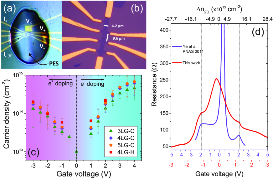
FLG flakes are prepared by micromechanical exfoliation of graphite on Si/SiO2NovoselovPNAS2005 ; BonaccorsoMatToday2012 . The number of layers, N, is determined by a combination of Raman spectroscopyFerrari2006 ; Ferrari_NNano2013 and optical microscopyCasiraghiNanoLett2007 . All FLGs are Bernal stacked. EDL field-effect devices are then prepared by electron beam lithography and deposition of Cr/Au contacts in the Hall bar configuration, as shown in Fig.1b. A coplanar gate contact is deposited on the side. A protective poly(methyl methacrylate) (PMMA) layer is spin-coated, patterned and hard-baked on the completed devices in order to avoid interactions between the electrolyte and the metallic leads. A reactive mixture precursor of the PES is then drop-cast onto the whole device and UV-cured, to get a cross-linked photopolymer electrolyteDaghero12 ; Gonnelli15 , Fig.1a. The precursor viscous liquid reactive mixture is composed of methacrylic oligomers and lithium salt: bisphenol A ethoxylate dimethacrylate (BEMA; average Mn: 1700, Aldrich), poly(ethylene glycol)methyl ether methacrylate (PEGMA; average Mn: 475, Aldrich), and 10% of lithium bis(trifluoromethanesulfonyl)imide (LiTFSI) along with the addition of 3 wt% 2-hydroxy-2-methyl-1-phenyl-1-propanon as the free radical photoinitiator (Darocur 1173, Ciba Specialty Chemicals). No annealing is performed in the time between contact deposition and PES casting, and the devices are stored in a desiccator under low vacuum (mbar) to prevent contamination. Four-wire resistance measurements are done under high vacuum (mbar) in the chamber of a Cryomech pulse-tube cryocooler via a Keithley 6221/2182A current source/nanovoltmeter assembly. The gate potential is controlled through a Keithley 2410 sourcemeter, whose negative electrode is set at the current drain contact. Gate leakage is monitored to ensure that no electrochemical reactions occur at the graphene/EDL interface. Magnetoresistance measurements are performed in an Oxford Instruments helium cryostat equipped with a superconducting magnet.
We estimate as a function of the gate voltage, VG, from the measured gate current through double-step chronocoulometryScholzInzelt (DSCC), as shown in Fig.1c for 3LG, 4LG and 5LG (green triangles, violet diamonds and orange pentagons, respectively) and described in detail in Ref.Gonnelli15 . This technique is based on the fact that, in absence of chemical reactions at the electrodes, the current flowing through the electrolyte can be split into two contributionsScholzInzelt . The first, due to the EDL build-up, decays exponentially over timeScholzInzelt . The second, due to ion diffusion through the bulk of the electrolyteScholzInzelt , decays as the square root of timeScholzInzelt . By fitting the gate current response to a step-like application and removal of VG with a function that separately accounts for both effects, the two contributions can be distinguished and, thus, the EDL charge estimated. Further details on the technique can be found in Refs.Daghero12 ; Gonnelli15 ; ScholzInzelt . These results are checked with independent Hall-effect measurements performed on a 4LG device (red squares in Fig.1c). We conservatively use the DSCC values in the full VG range.
We also compare the RT resistance as a function of VG in a 3LG with the earlier measurements of Ref.YePNAS . Fig.1d shows how, in both cases, regions of sharp non-monotonic behavior are present in the resistance curves away from the Dirac point. The position of these upturns is associated with a specific charge density, such that the Fermi level, EF is crossing the bottom of the split-off bandsYePNAS , and this fact can be used for voltage-carrier density calibration. This comparison indicates that our PES allows us to reach the split-off bands at lower potential than the ionic liquid of Ref.YePNAS , thus supporting a higher charge induction capability.
III Results and Discussion
We first measure the four-contact resistance in the 4-290K range as a function of N and . In each measurement, VG is applied at RT and the sample is then cooled to a base T4-10K, depending on sample. Any further modification of below the PES glass transition at230KGonnelli15 is prevented by the quenched ion motionUeno08 ; Ye12 . The samples are then allowed to spontaneously warm up, taking advantage of the absence of T fluctuations associated with the cryocooler’s thermal cycles. We reported a detailed analysis of the T dependence of RS for these device in the 30-290K range in Ref.Gonnelli15 . Here we focus on the anomalous behavior that emerges in the 4-30K range.
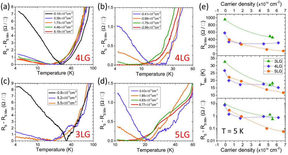
For all the three N, a logarithmic upturn is observed for TK in the resistance curves for samples in the metallic regime, as shown in Fig.2. Figs.2a-d plot the low-T ( K) variations of RS with respect to its minimum value RSMin for 3LG, 4LG and 5LG as function of T in a semi-logarithmic scale. RSMin decreases with increasing n2d for all N, and saturates for 4LG (see top panel of Fig.2e). Both the amplitude of the logarithmic upturn (RRSMin) and the TMin at which RSMin is reached strongly depend on and N, as shown in the central and bottom panels of Fig.2e. Similar logarithmic upturns in the resistance of conductors in the diffusive regime, such as Si MOSFETsWheelerPRL1982 , GaAs heterostructuresChoiPRB1986 ; Hansen , and transition metal alloysSarachikPR1964 are usually attributed to Kondo effectKondo1964 , WLBergmannWL ; LarkinWL , and electron-electron (e-e) interactionsAltshuler_elinter ; Altshuler_elinter_Rev ; FukuyamaEE , or to a superposition of any of the previous sourcesBeenakkerWL .
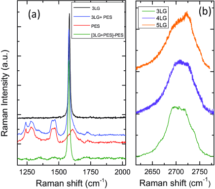
We first consider the Kondo effect, which is caused by carrier scattering from diluted magnetic impuritiesSarachikPR1964 ; Kondo1964 . Unlike Ref.ChenKondo , we do not intentionally introduce any defect in our samples. We thus employ Raman spectroscopy to monitor the amount of Raman active defects in our devices, before and after PES drop-casting. Raman measurements are carried out at RT in a Renishaw InVia microspectrometer equipped with a 100X objective. The spot size ism, the excitation wavelength is 514nm and the incident power is kept well below 1mW in order to avoid heating. Fig.3a shows the Raman spectrum of a 3LG device. The PES shows several peaks between1000 and 1500cm-1. The broad peak between1400 and 1500cm-1 can be assigned to the methylene bending modeReyElecActa1998 , the peak at1280cm-1 to methylene twistingChrissopoulouMacmol2011 , and that at1243cm-1 to either trifluoromethyl stretchingReyElecActa1998 or methylene twistingChrissopoulouMacmol2011 .
We perform a background subtraction by normalizing to the low-frequency PES peaks near the D peak. This gives an upper limit for the ratio between the intensity of the D peak and the intensity of the G peak, I(D)/I(G),0.015, which leads to an estimated maximum defect densitycm-2CancanoNanoLett2011 ; BrunaACSNano2014 . For comparison, in order to obtain a sizeable Kondo effect ( at T=0.3K), in Ref.ChenKondo it was necessary to induce a defect densitycm-2, which produced a corresponding I(D)/I(G)3.8ChenKondo . Our values indicate that our devices are at least two orders of magnitude less defective, and we thus discard the possibility of a contribution from Kondo effect to the resistance upturn.
III.1 Weak Localization in Few-layer Graphene
WL arises from the constructive interference between pairs of time-reversed trajectories of electrons elastically scattering in a closed loopBeenakkerWL . This increases the probability of charge-carrier backscattering in a conductor in the diffusive regimeBergmannWL ; LarkinWL , thus reducing the conductanceBeenakkerWL . In order for WL to appear, phase coherence must be maintained throughout the entire closed loop followed by the electrons undergoing the elastic scattering that is described by a characteristic lifetime BergmannWL . WL is thus suppressed by an increased probability of inelastic scattering associated with the T increaseBergmannWL . The average time interval in which phase coherence is maintained is called phase coherence lifetime BeenakkerWL . Typically, two inelastic processes determine BeenakkerWL . Electron-phonon (e-ph) scatteringTaboryski , which is important for higher TBeenakkerWL , and electron-electron (e-e) scatteringNarozhny ; Altshuler_elscat , which dominates for lower TBeenakkerWL . The T that marks a crossover between these two scattering processes depends on the transport properties of each materialBeenakkerWL , and it is typically of the order of few tens KBeenakkerWL .
In a diffusive system a conductivity suppression at low T may also be caused by e-e interactions, as a result of the diffraction of an electron wave by the oscillations in the electrostatic potential generated by the other electronsBeenakkerWL ; Altshuler_elinter ; Altshuler_elinter_Rev ; FukuyamaEE . A widely exploited approach to discriminate between these two contributions is the measurement of the sample magnetoconductanceBeenakkerWL ; Altshuler_elinter ; Altshuler_magnetoR . In the presence of a perpendicular magnetic field B, time-reversal symmetry is brokenBeenakkerWL . A phase difference arises between any two time-reversed electron trajectories, whose constructive interference, in principle able to localize electronsBeenakkerWL , is therefore brokenAltshuler_magnetoR . As a consequenceBeenakkerWL : i) a negative magnetoconductance is associated with WALHikami_WLB ; ii) a vanishing magnetoconductance is associated with e-e interaction (insensitive to B)Altshuler_magnetoR ; iii) a positive magnetoconductance is associated with WLAltshuler_magnetoR ; Hikami_WLB .
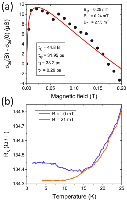
In order to determine the origin of the resistance upturn we thus measure the magnetoconductance of a 3LG device at 2K. We find it positive, and reaching a maximum at T, as shown in Fig.4a, where the magnetoconductance relative to the value at zero field is plotted as a function of B. In order to rule out even a partial contribution from e-e interactions, we also measure the device resistance while heating the sample under . Fig.4b shows that the logarithmic upturn is suppressed within the noise level. This behavior is reversible upon removal of B. The logarithmic upturn saturates for 4K, a feature usually assigned to the effect of finite channel sizeTikhonenko09 . These data support the conclusion that, in our devices, WL is the source of the measured resistance upturn and that the logarithmic correction to the conductivity due to e-e interaction can be disregarded. This is in contrast with earlier reports on SLG, where both contributions were shown to be relevantKozikovPRB2010 .
The carrier lifetimes determine the WL behaviorBeenakkerWL ; Hikami_WLB , and can thus be obtained from Fig.4aMcCann06 ; Falko07 . In SLG it was predicted that, due to lattice symmetries, an additional Berry phase is accumulated by charge carriers scattering in closed loopsZhang05 ; Suzuura02 ; Suzuura03 . In 2LG such additional Berry phase is instead Novoselov06 ; Falko07 . This means that in SLG the quantum interference due to localization is always destructiveAndo98 ; Ando2005 , leading to an anti-localization behaviorHikami_WLB , while in 2LG the effect of the additional phase cancels out, and the material should retain the standard WL behaviorFalko07 . In addition, WAL, where the underlying elastic scattering mechanism is due to charged impurities, is strongly suppressed by intervalley scattering and trigonal warpingMcCann06 . Furthermore, Refs.McCann06 ; Falko07 showed that SLG and 2LG have a further quantum correction to the Drude resistivity, always localized, due to elastic intervalley scattering, and not affected by trigonal warping. As a consequence, various localization behaviors were reportedTikhonenko09 ; Tikhonenko08 ; Hikami_WLB ; Wu07 ; Berger06 ; Morozov06 ; Ki08 ; Liao10 , depending on the sample preparation and on the explored regime.
To the best of our knowledge, a WL model for has not yet been developed. Earlier WL reports in FLG made use of models developed for SLG and 2LGLiuPCCP2011 ; WangCarbon2012 ; ChuangCurrApplPhys2014 . Furthermore, the simultaneous presence of both Dirac-like and parabolic bands in odd-N flakesNakamura08 ; Koshino10 makes an a-priori determination of the total Berry phase difficult. Here we show that the correction to the conductance due to the Berry phase is suppressed in all our experiments. This allows us to conclude that only elastic intervalley scattering is relevant for quantum interference.
Following the theoretical approach of Ref.Falko07 , the T dependence of the quantum correction to the 2d conductance is determined by the T behavior of the phase coherence lifetime , as:
| (1) |
where is the intervalley scattering lifetime, is the transport lifetime (associated with scattering from charged impuritiesTikhonenko09 ; Tikhonenko08 ) and is an effective lifetime associated with intravalley scattering and trigonal warping. On the right hand side of Eq.1, the first term arises from intervalley scattering, and resembles the conventional weak localization correctionBeenakkerWL , apart from the factor two and the different elastic lifetime involved. Since the argument of the logarithm is always greater than one, this term is always negative. The second term, arising from intravalley scattering, is positive or negative depending on the Berry phase, and is strongly suppressed the larger the value of McCann06 ; Falko07 . The B dependence of the quantum correction to the conductance can be written asMcCann06 ; Falko07 :
| (2) |
where:
and
being the digamma functionFalko07 , the diffusion coefficientFalko07 , and the Fermi velocity. We obtain by combining the measurement of with ab-initio DFT calculations (see Eq.7). This gives the values fs and cm2s-1 that will be used in later calculations.
For the data in Fig.4a (3LG), the Berry phase is and . We therefore use Eq.2 to fit as a function of B in the 0-0.2T range (red solid curve in Fig.4a). This gives ps, ps and ps. Thus, we are in the condition , where the zero-field antilocalization term is suppressed to the point of being negligibleMcCann06 ; Falko07 .
We can compare these results with the existing literature at T=4K, immediately before the signal saturation for T4K, shown in Fig.4b. Ref.Tikhonenko08 presents a WL study in SLG for different carrier densities, expressed in terms of the characteristic lengthscales . For cm-2 and T=4K, they report m, m and nm. This is the value of closest to that in our devices, even if still at least one order of magnitude smaller. The characteristic lifetimes in our device give m, m and nm, in agreement with the existing dataTikhonenko08 .
Since the T dependence of contains information on the most relevant inelastic scattering mechanismsBeenakkerWL ; Hikami_WLB and following the previous results, we can use Eq.1 with to describe the low-T (20-30K) part of the as a function of T curves in Fig.2. This approach is sound, since the smallest doping in our measurements iscm-2, a large value for solid-dielectric gating experimentsUenoReview2014 ; FujimotoReview2013 , and we do not find anti-localized behavior at these doping levels. Refs.Tikhonenko09 ; Tikhonenko08 ; Baker_lphi also reported that doping strongly enhances (thus reducing ), since trigonal warping becomes more relevant the higher the energy separation from the Dirac point. This makes our approximation valid also for higher doping.
We can thus write the complete expression for the conductance of our FLG devices, valid for TK:
| (3) |
where isCappelluti_sigma :
| (4) |
Here and are the valley and spin degeneracies, respectively, is the Fermi velocity and the DOS at the Fermi level of the i-th band. Taking into account the Matthiessen ruleMatthiessenRule on the carrier lifetime at finite T we have:
| (5) |
where is the T-dependent inelastic scattering lifetime. Substituting in Eq. 3 we get:
| (6) |
In order to proceed further, we need to determine the prefactor , the transport lifetime and the T dependence of .
We estimate by computing the FLG bandstructure through ab-initio Density Functional Theory (DFT) for all our doping levels. We also perform a consistency check of the DFT estimations by running independent self-consistent tight-binding calculations for the doped 4LG. Here we present the results for Bernal stacked 4LG and 5LG. As a first approximation, we assume these systems to be isolated, i.e. we consider the effects of the substrate to be negligible.
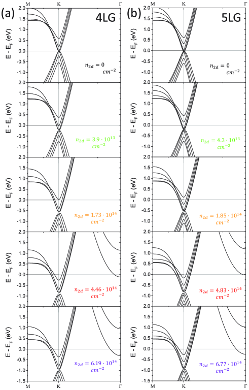
We first investigate the band-structures of FLG within the all-electron, full-potential, linear augmented plane wave (FP-LAPW) method as implemented in the ELK codeELK . The local density approximation (LDA)Perdew81 is used to describe the exchange and correlation. We fix the in-plane lattice constant to a=2.46Å, i.e. the experimental in-plane lattice constant of graphiteSlonczewskiPR1958 . To model FLG we consider a three-dimensional supercell with a very high value of the c lattice constant so that the periodic images of the structures are at least 10Å apart, in order to avoid interactions (e.g., for 4LG we take c=40a.u.) while the layer-layer distance is taken to be 3.35Å independent of N. Doping is simulated by adding electrons to the systems, together with a compensating positive background, as in Refs.GeLiu ; Margine14 (Jellium model). The Brillouin zone is sampled with a k-point mesh. The radius of the muffin-tin spheres for the carbon atoms are taken as 1.342, where is the Bohr radius. We set RMTKmax=8, where RMT is the smallest muffin-tin radius, Kmax is a cutoff wave vector and the charge density is Fourier expanded up to a maximum wave vector G. The convergence of self-consistent field calculations is attained with a total energy tolerance of Hartree.
Fig.5 plots the results for both 4LG (panel a) and 5LG (panel b) for different doping. The extra induced charge shifts EF away from the Dirac point, eventually crossing multiple bands at K and K’. In all cases, the crossing occurs well within regions where the energy dispersion is nearly linear. For the highest VG (+3 and +4V), however, an additional important feature appears in the bandstructure. The large induced charge density brings down a further band at , which becomes populated and can thus contribute to the transport properties. The dispersion of this new band is fully parabolic, and its appearance is reminiscent of that of the interlayer band induced by alkali metal intercalation in graphite intercalated compounds (GICs)Profeta12 .
Our approach neglects the intense electric field at the EDL/graphene interface, that in transition-metal dichalcogenides increases with doping and affects the effective mass valueBrumme15 . The simplified Jellium model was shown to capture the fundamental physics of doped SLGMargine14 and single-layer MoS2GeLiu . We thus perform a consistency check for 4LG by comparing DFT with tight-binding calculations where the screening of the electric field by the charge carriers is accounted for. We compare the same terms , where represent the band index, are the Fermi velocities and are the density of the state at EF. The and values obtained by tight-binding and DFT are within 30%. This suggests that our DFT approach is correct at least to a first-order approximation.
These calculations allow us to obtain both the DOS and the electron velocity of the populated bands at EF which, in turn, according to Eq.4, determine . Once is known, can be evaluated. Fig.4b shows that, in the absence of WL, the resistance saturates to a constant value for T8K. Thus, the saturation Boltzmann conductance can be estimated from the minimum RSMin before the onset of the logarithmic upturn. This underestimates the saturation conductance (and thus the scattering time) by less than 1%, which is negligible compared to the other sources of uncertainty in the evaluation of . This approach allows us to compute as a function of n2d in all our devices as:
| (7) |
III.2 Scattering lifetimes vs. Temperature
We now consider the T dependence of . This can be done by using Eq.1 without the contribution (since ) in the analysis of the low-T part (4T20K) of the curves of Fig.2. By inverting this simplified expression, we obtain the T dependence of , as shown in Fig. 6a (4LG) and b (5LG). Since , for T30K, can be assumed almost independent of TTikhonenko08 , the T dependence of is the same as that of . By expressing , we associate the p value to specific scattering processes. For T lower than the Bloch-Gruneisen THwangPRB2008 , e-ph scattering gives p=3 for a standard 2-dimensional electron gas (2DEG)Taboryski and p=4 for SLGHwangPRB2008 . The e-e scattering gives p=1 for the Nyquist (small momentum exchange) processAltshuler_elscat and p=2 for the Coulomb (large momentum exchange) processNarozhny . As shown in Fig.6, the curves show almost no superlinear behavior in the WL region. Nyquist e-e scattering is thus the dominant mechanism in this T range. This is consistent with the existing literature on SLGTikhonenko09 and 2LGGorbachevPRL2007 ; ChenPhysicaB2011 . In Ref.Gonnelli15 we reported that the T dependence below 100K has a linear plus a quadratic contribution, the linear being dominant for T30K (see Figs.4a,5c of Ref.Gonnelli15 ) and assigned this to competing Coulomb and Nyquist e-e scattering processes. This is consistent with the present observation of a dominant Nyquist contribution for T20K. Thus, since is determined by the inelastic scattering lifetime BeenakkerWL , we can write the T dependence of in the entire 4-90K range as:
| (8) |
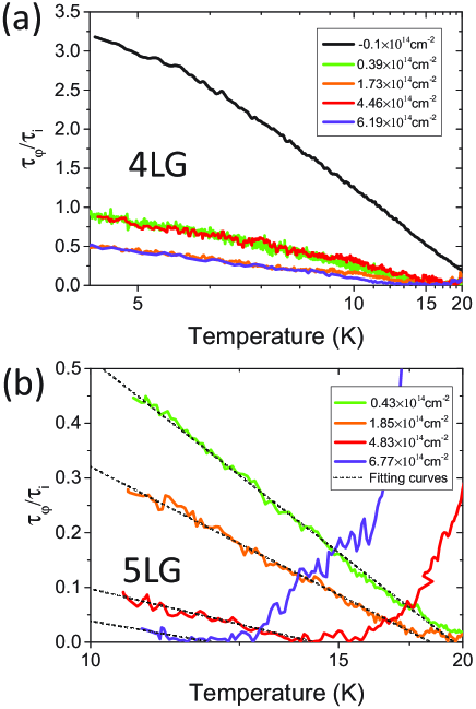
By inserting Eq.8 in the first terms of the Drude conductance of Eq.6, we can fit the curves at different doping in the intermediate T region (30-90K) where the WL contribution can be neglected. With the previously determined values of and , this fit provides us the parameters and . Finally, combining determined here with obtained from the low T (4-20K) region, we can extract . Fig.6b shows the excellent agreement between the fitting model (black dashed lines) and the experimental data in the WL region (solid lines).
We first apply this procedure to the RS as a function of T curves of the device on which the magnetoresistance was measured, obtaining ps and ps at 4K, in agreement with the values coming from the magnetoresistance fit at 2K. Once again, the comparison is carried out at 4 instead of 2K due to the signal saturation for T4K in Fig.4b. This analysis is then repeated on the 4LG and 5LG devices for different values of the applied gate voltage.
III.3 Scattering lifetimes vs. Carrier density
We now discuss the measured trends of , and as a function of .
In standard 2DEGs, such as GaAs heterostructuresHansen , is equivalent to the elastic scattering lifetime and is found to follow a dependence on of the type Hansen ; PaalanenPRB1984 ; WalukiewiczPRB1984 . This implies that increases for increasing due to the increased screening of elastic scatterers by the increased density of charge carriersGiuliani05 ; Mahan00 . In our devices, however, does not follow this behavior, suggesting a significant increase of the number of elastic scatterers with increasing gate voltage.
If we consider the 4LG device first, we observe that shows a monotonically decreasing behavior (Fig.7a, blue dots). One possible explanation was suggested in Ref.DasSarma14 , where the authors reported a decreasing mobility at high for 2DEGs: In contrast to Coulomb disorder, short-range disorder would become stronger with increasing , thus increasing the scattering rateDasSarma14 . However, we think that this is not the main source of the increase of in our case. A degradation of the mobility of EDL-gated devices was reported in strontium titanateGallagherNComms2015 and rhenium disulfideOvchinnikovNComms2016 , where it was suggested that ions in the electrolyte act as charged impurities. Thus, we attribute this effect to the microscopic dynamics of how EDL gating induces extra carriers in the material. EDL gating is able to induce modulations in excess of 1014cm-2 to the charge carrier density of a material by accumulating a densely packed layer of ions in close proximity (1nmUenoReview2014 ; FujimotoReview2013 ) to its surface. Refs.Zhang09 ; StrasserNanoLett2015 reported that charge-donating impurities at the SLG surface act as scattering centers.
We thus propose that the Li+ ions in the EDL perform a similar role. Their increased density with VG competes with the increased screening induced by the extra carriers and this determines . In 4LG, the former effect would be stronger in the entire range, resulting in the monotonic reduction of . If this is the case, we expect 5LG to be less sensitive to the extra scattering centers. These are localized at the surface of the first layer, and Ref.GallagherNComms2015 showed that introducing a thin spacer between the ions and the conductive channel greatly improves carrier mobility. With respect to 4LG, 5LG features one further conductive channel due to the fifth SLG, which is thus further separated from the scattering centers. Indeed, this is what we observe: The 5LG device shows an initial decrease for cm-2 followed by an increase for cm-2 (Fig.7b, blue dots). Overall, the in 5LG is nearly constant with the carrier density, as if the two competing effects on the carrier mobility were almost canceling out.
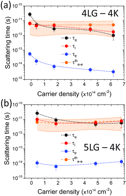
Let us now consider the doping dependence of and in 4LG and 5LG, in order to allow for a direct comparison with the corresponding values for 3LG estimated from magnetoresistance. Fig.7 shows that the doping dependence of is weakly decreasing or nearly constant within the uncertainty range: from ps to ps for 4LG, from ps to ps for 5LG. This dependence was already observedTikhonenko09 ; Baker_lphi , albeit for cm-2, much lower than the carrier densities considered here (cm-2). In contrast, the doping dependence of is more significant, as it is monotonically decreasing in the entire range in 4LG, while it shows a small inversion in slope on the final point for 5LG. These results are in contrast with earlier findings on FLG for cm-2Baker_lphi . As already pointed out, e-e Nyquist scattering is the dominant dephasing mechanism in the low T range. Therefore, we can writeHansen :
| (9) |
The condition (Ioffe-Regel criterionIoffeRegel ) characterizes the Anderson metal-to-insulator transitionMottDavis . The metallic regime corresponds to , leading to a increasing with (i.e. with increasing EF). Under strong localization conditions, x1 and the Boltzmann model no longer holdsAndersonPR1958 . Intermediate x values mark a crossover from strong to weak localizationMottBook and correspond to a region where can present a decreasing behavior with . The exact form of the curves is determined by the dependence of EF with (which, in the linear regions of the bands, is a square rootCastroNetoReview ) and by . If we compute x corresponding to our data by using the values determined at 4K, we find that for 4LG x=2.70.2 in the entire range of negative charge induction, while for 5LG x2.7 for VG=1 and 2V, x5 for V and 4V. Thus, the 4LG device is always in the ”crossover” condition, while in 5LG the typical 2DEG behavior is restored for cm-2. Due to the dependence of x on , these results are consistent with the fact that the ion dynamics in the EDL gating provides a competition between an increase of the number of elastic scattering center and of at the increase of VG. In 4LG the concurrent increase of EF and decrease of (see Fig.7a) could maintain x almost constant. In 5LG at cm-2 the increase of both EF and (see Fig.7b) would eventually lead to the increase of x. This particular behavior could be due to the differences in both surface-to-volume ratio and bandstructure of 4LG and 5LG, and is in agreement with the behavior of in the two samples.
In order to further analyze these results, we evaluate the theoretical values of the e-e scattering lifetimes by using the definition of x given in Eq.9 with determined by DFT and taken from the determined values. The results are shown in Figs.7 as orange circles and shaded bands (that represent the uncertainty regions). Our (black dots) are in agreement with the theoretical predictions within an order-of-magnitude. However, the latter are nearly doping-independent in contrast with experiments. This different behavior is particularly evident in 4LG. As expected, the addition of the Coulomb scattering termTikhonenko09 does not affect appreciably the predicted values at this low T. Since the theoretical are dependent on the details of the ab-initio calculations, the inconsistency might be related to the approximations employed in the DFT calculations of the effects of the high electric field. Another reason for the mismatch could be the validity of the hypotheses underlying the theoretical derivation of the Nyquist scattering. In particular, both the single-band and the parabolic-dispersion assumptions do not hold in FLG, particularly when the Fermi level is so far from the Dirac pointNakamura08 ; Koshino10 .
A comparison with the other experimental technique able to probe the e-e scattering lifetime, i.e. pump-probe spectroscopy, is not immediate, due to the different conditions in the probed electron system between transport and spectroscopic measurements. Low-bias (VLazzeriPRL2005 ) transport measurements, such as the ones performed in this work, involve only scattering processes between carriers very close to the Fermi level. Pump-probe measurements, on the other hand, generate a strongly out-of-equilibrium carrier population by optical excitation. This population first thermalizes to a quasi-equilibrium distribution of ”hot” carriers via e-eBridaNComms2013 ; BreusingPRB2011 ; ObraztsovNanoLett2011 and e-optical phononsLazzeriPRL2005 ; BridaNComms2013 ; LuiPRL2010 ; BreusingPRB2011 ; SunPRL2008 ; HuangNanoLett2010 scattering processes. The ”hot” carriers then cool down to the rest of the Fermi sea over a much longer time scale by scattering with optical phononsLazzeriPRL2005 ; BridaNComms2013 ; LuiPRL2010 ; BreusingPRB2011 ; SunPRL2008 ; HuangNanoLett2010 ; ObraztsovNanoLett2011 . This makes the two types of measurements hardly comparable, as the e-e scattering lifetime is heavily dependent on the distance in energy between the scattering electrons and the Fermi levelLiPRB2013 ; HwangPRB2007 . Moreover, pump-probe experiments are typically performed at room TBridaNComms2013 ; LuiPRL2010 ; BreusingPRB2011 ; HuangNanoLett2010 ; ObraztsovNanoLett2011 , where the Coulomb term dominates the e-e scattering, while our experiments are performed at low T, where the Nyquist term dominates instead. Even with all these caveats, we can try to extrapolate to room T the e-e scattering lifetimes in our systems using Eq.9 and imposing T=300K. This gives extrapolated room T between 1 and 7fs, in agreement with existing literatureBridaNComms2013 ; BreusingPRB2011 ; ObraztsovNanoLett2011 .
IV Conclusions
We explored the electronic transport properties of 3-, 4- and 5-layer graphene in the doping regime in excess ofcm-2 and in the 4-30K temperature range. We used electric double layer gating to dope the samples up tocm-2. We found evidence of quantum coherent transport in the entire carrier density range. Magnetoresistance measurements showed that, in the 4-30K range, transport is dominated by weak localization in the diffusive regime, and that the behavior of 3LG, 4LG and 5LG is described by the theoretical models developed for SLG and 2LG. We combined the experimental results with DFT calculations to determine the carrier scattering lifetimes as a function of the carrier density for different number of layers, and determined that electron-electron scattering with small momentum transfer (Nyquist process) is the main source of dephasing at low temperatures. Both the transport scattering lifetime and the phase coherence lifetime show a non-trivial dependence on n2d. We explained the behavior of in terms of a competing modulation of doping and density of charged scattering centers induced by EDL gating. The doping dependence of points to a gate-tunable crossover from weak to strong localization, highlighting the limits of applying single-band models to multi-band systems, such as heavily doped few-layer graphene.
V Acknowledgments
We thank M. Calandra, M. Polini and V. Brosco for useful discussions. We acknowledge funding from EU Graphene Flagship, ERC Grant Hetero2D, EPSRC Grant Nos. EP/ 509K01711X/1, EP/K017144/1, EP/N010345/1, EP/M507799/ 5101, and EP/L016087/1 and the Joint Project for the Internationalization of Research 2015 launched by Politecnico di Torino under funding of Compagnia di San Paolo.
References
- (1) M. J. Panzer, C. R. Newman, and C. D. Frisbie, Low-voltage operation of a pentacene field-effect transistor with a polymer electrolyte gate dielectric. Appl. Phys. Lett. 86, 103503 (2005).
- (2) M. Bayer, C. Uhl, and P. Vogl, Theoretical study of electrolyte gate AlGaN/GaN field effect transistors. J. Appl. Phys. 97, 033703 (2005).
- (3) H. T. Yuan, H. Shimotani, A. Tsukazaki, A. Ohtomo, M. Kawasaki, and. Y. Iwasa, High-density carrier accumulation in ZnO field-effect transistors gated by electric double layers of ionic liquids. Adv. Funct. Mater. 19, 1046-1053 (2009).
- (4) K. Ueno, S. Nakamura, H. Shimotani, A. Ohtomo, N. Kimura, T. Nojima, H. Aoki, Y. Iwasa, and M. Kawasaki, Electric-field-induced superconductivity in an insulator. Nature Mater. 7, 855-858 (2008).
- (5) J. T. Ye, S. Inoue, K. Kobayashi, Y. Kasahara, H. T. Yuan, H. Shimotani, and Y. Iwasa, Liquid-gated interface superconductivity on an atomically flat film. Nature Mater. 9, 125-128 (2009).
- (6) J. T. Ye, Y. J. Zhang, R. Akashi, M. S. Bahramy, R. Arita, and Y. Iwasa, Superconducting dome in a gate-tuned band insulator. Science 338, 1193 (2012).
- (7) K. Ueno, H. Shimotani, H. T. Yuan, J. T. Ye, M. Kawasaki and Y. Iwasa, Field-induced superconductivity in electric double layer transistors. J. Phys. Soc. Jpn. 83, 032001 (2014).
- (8) T. Fujimoto and K. Awaga, Electric-double-layer field-effect transistors with ionic liquids. Phys. Chem. Chem. Phys. 15, 8983 (2013).
- (9) A. M. Goldman, Electrostatic Gating of Ultrathin Films. Annu. Rev. Mater. Res. 44, 45 (2014).
- (10) Y. Saito, T. Nojima, and Y. Iwasa, Gate-induced superconductivity in two-dimensional atomic crystals. Supercond. Sci. Technol. 29, 093001 (2016).
- (11) A. Das et al., Monitoring dopants by Raman scattering in an electrochemically top-gated graphene transistor. Nature Nanotech. 3, 210 (2008).
- (12) A. Das, B. Chakraborty, S. Piscanec, S. Pisana, A. K. Sood, and A. C. Ferrari, Phonon renormalization in doped bilayer graphene. Phys. Rev. B. 79, 155417 (2009).
- (13) F. Chen, Q. Qing, J. L. Xia, J. H. Li, and N. J. Tao, Electrochemical gate-controlled charge transport in graphene in ionic liquid and aqueous solution. J. Am. Chem. Soc. 131, 9908 (2009).
- (14) A. Pachoud, M. Jaiswal, P. K. Ang, K. P. Loh and B. Ozyilmaz, Graphene transport at high carrier densities using a polymer electrolyte gate. Europhys. Lett. 92, 27001 (2010).
- (15) D. K. Efetov and P. Kim, Controlling electron-phonon interactions in graphene at ultrahigh carrier densities. Phys. Rev. Lett. 105, 256805 (2010).
- (16) C. H. Lui, Z. Q. Li, K. F. Mak, E. Cappelluti and T. F. Heinz, Observation of an electrically tunable band gap in trilayer graphene. Nature Phys. 7, 944 (2011).
- (17) J. T. Ye, M. F. Craciun, M. Koshino, S. Russo, S. Inoue, H. T. Yuan, H. Shimotani, A. F. Morpurgo, and Y. Iwasa, Accessing the transport properties of graphene and its multilayers at high carrier density. Proc. Natt. Acad. Sci. USA 108, 32 (2011).
- (18) Z. Y. Chen, H. T. Yuan, Y. F. Zhang, K. Nomura, T. Gao, y. Gao, H. Shimotani, Z. F. Liu, and Y. Iwasa, Tunable Spin–Orbit Interaction in Trilayer Graphene Exemplified in Electric-Double-Layer Transistors. Nano Lett. 12, 2212 (2012).
- (19) E. H. Hwang and S. Das Sarma, Acoustic phonon scattering limited carrier mobility in two-dimensional extrinsic graphene. Phys. Rev. B 77, 115449 (2008).
- (20) S. H. Jo, D. Costanzo, H. Berger, and A. F. Morpurgo, Electrostatically induced superconductivity at the surface of WS2. Nano Lett. 15, 2 (2015).
- (21) D. Daghero, F. Paolucci, A. Sola, M. Tortello, G. A. Ummarino, M. Agosto, R. S. Gonnelli, J. R. Nair, and C. Gerbaldi, Large conductance modulation of gold thin films by huge charge injection via electrochemical gating. Phys. Rev. Lett. 108, 066807 (2012).
- (22) M. Tortello, A. Sola, K. Sharda, F. Paolucci, J. R. Nair, C. Gerbaldi, D. Daghero, and R. S. Gonnelli, Huge field-effect surface charge injection and conductance modulation in metallic thin films by electrochemical gating. Appl. Surf. Sci. 269, 17 (2013).
- (23) R. S. Gonnelli, F. Paolucci, E. Piatti, K. Sharda, A. Sola, M. Tortello, J. R. Nair, C. Gerbaldi, M. Bruna, and S. Borini, Temperature Dependence of Electric Transport in Few-layer Graphene under Large Charge Doping Induced by Electrochemical Gating. Sci. Rep. 5, 9554 (2015).
- (24) G. Profeta, M. Calandra and F. Mauri, Phonon-mediated superconductivity in graphene by lithium deposition. Nature Phys. 8, 131 (2012).
- (25) J. Delahaye J. Hassel, R. Lindell, M. Sillanpää, M. Paalanen, H. Seppä, and P. Hakonen, Low-Noise Current Amplifier Based on Mesoscopic Josephson Junction. Science 299, 1045 (2003).
- (26) S. De Franceschi, L. Kouwenhoven, C. Schönenberger, and W. Wernsdorfer, Hybrid superconductor–quantum dot devices. Nature Nanotech. 5, 703 (2010).
- (27) M. Huefner, C. May, S. Kicin, K. Ensslin, T. Ihn, M. Hilke, K. Suter, N. F. de Rooij, and U. Staufer, Scanning gate microscopy measurements on a superconducting single-electron transistor. Phys. Rev. B 79, 134530 (2009).
- (28) E. R. Margine and F. Giustino, Two-gap superconductivity in heavily n-doped graphene: Ab initio Migdal-Eliashberg theory. Phys. Rev. B 90, 014518 (2014).
- (29) B. M. Ludbrook et al., Evidence for superconductivity in Li-decorated monolayer graphene. Proc. Natl. Acad. Sci. USA 112, 11795 (2015).
- (30) S. Ichinokura, K. Sugawara, A. Takayama, T. Takahashi, and S. Hasegawa, Superconducting Calcium-Intercalated Bilayer Graphene. ACS Nano 10, 2761 (2016).
- (31) M. Bruna and S. Borini, Optical constants of graphene layers in the visible range. Appl. Phys. Lett. 94, 031901 (2009).
- (32) C. H. Lui, Z. Q. Li, Z. Y. Chen, P. V. Klimov, L. E. Brus, and T. F. Heinz, Imaging stacking order in few-layer graphene. Nano Lett. 11, 164 (2011).
- (33) K. S. Novoselov, D. Jiang, F. Schedin, T. J. Booth, V. V. Khotkevich, S. V. Morozov, and A. K. Geim, Two-dimensional atomic crystals. Proc. Natl. Acad. Sci. USA 102, 10451 (2005).
- (34) F. Bonaccorso, A. Lombardo, T. Hasan, Z. P. Sun, L. Colombo, and A. C. Ferrari, Production and processing of graphene and 2d crystals. Mater. Today 15, 564 (2012).
- (35) A. C. Ferrari and D. Basko, Raman spectroscopy as a versatile tool for studying the properties of graphene. Nature Nanotech. 8, 235 (2013).
- (36) A. C. Ferrari et al., Raman spectrum of graphene and graphene layers. Phys. Rev. Lett. 97, 187401 (2006).
- (37) C. Casiraghi, A. Hartschuh, E. Lidorikis, H. Qian, H. Harutyunyan, T. Gokus, K. S. Novoselov, and A. C. Ferrari, Rayleigh imaging of graphene and graphene layers. Nano Lett. 7, 2711 (2007).
- (38) M. Bruna, A. K. Ott, M. Ijas, D. H. Yoon, U. Sassi, and A. C. Ferrari, Doping dependence of the Raman spectrum of defected graphene. ACS Nano 8, 7432 (2014).
- (39) L. G. Cancado, A. Jorio, E. H. Martins Ferreira, F. Stavale, C. A. Achete, R. B. Capaz, M. V. O. Moutinho, A. Lombardo, T. S. Kulmala, and A. C. Ferrari, Quantifying defects in graphene via Raman spectroscopy at different excitation energies. Nano Lett. 11, 3190 (2011).
- (40) C. X. Cong†, T. Yu, K. Sato, J. Z. Shang, R. Saito, G. F. Dresselhaus, and M. S. Dresselhaus, Raman characterization of ABA-and ABC-stacked trilayer graphene. ACS Nano, 11, 8760 (2011).
- (41) A. C. Ferrari, Raman spectroscopy of graphene and graphite: disorder, electron–phonon coupling, doping and nonadiabatic effects. Solid State Commun. 143, 47-57 (2007).
- (42) F. Scholz and G. Inzelt, Electroanalytical Methods (2nd ed.), 147-158 (2010).
- (43) T. Brumme, M. Calandra and F. Mauri, First-principles theory of field-effect doping in transition-metal dichalcogenides: Structural properties, electronic structure, Hall coefficient, and electrical conductivity. Phys. Rev. B 91, 155436 (2015).
- (44) R. G. Wheeler, K. K. Choi, A. Goel, R. Wisnieff, and D. E. Prober, Localization and electron-electron interaction effects in submicron-width inversion layers. Phys. Rev. Lett. 49, 1674 (1982).
- (45) K. K. Choi, D. C. Tsui, and S. C. Palmateer, Electron-electron interactions in GaAs-AlxGa1−xAs heterostructures. Phys. Rev. B 33, 8216 (1986).
- (46) J. E. Hansen, R. Taboryski, and P. E. Lindelhof, Weak localization in a GaAs heterostructure close to population of the second subband. Phys. Rev. B. 47, 16040 (1993).
- (47) M. P. Sarachik, E. Corenzwit, and L. D. Longinotti, Resistivity of Mo-Nb and Mo-Re Alloys Containing 1% Fe. Phys. Rev. 135, A1041 (1964).
- (48) J. Kondo, Resistance minimum in dilute magnetic alloys. Prog. Theor. Phys. 32, 37 (1964).
- (49) G. Bergmann, Weak localization in thin films: a time-of-flight experiment with conduction electrons. Phys. Rep. 107, 1 (1984); Physical interpretation of weak localization: A time-of-flight experiment with conduction electrons. Phys. Rev. B 28, 2914 (1983).
- (50) A. I. Larkin and D. E. Khmelnitsky, Anderson localization and anomalous magnetoresistance at low temperatures. Usp. Fiz. Nauk 136, 536 (1982) [Sov. Phys. Usp. 25, 185 (1982)].
- (51) J. H. Chen, L. Li, W. G. Cullen, E. D. Williams, and M. S. Fuhrer, Tunable Kondo effect in graphene with defects. Nature Phys. 7, 535-538 (2011).
- (52) C. W. J. Beenakker and H. van Houten, Quantum transport in semiconductor nanostructures. Solid State Phys. 44, 1 (1991).
- (53) B. L. Altshuler, A. G. Aronov, and P. A. Lee, Interaction effects in disordered Fermi systems in two dimensions. Phys. Rev. Lett. 44, 19 (1980).
- (54) B. L. Altshuler and A. G. Aronov, in Electron-Electron Interactions in Disordered Systems, p. 1 (A. L. Efros and M. Pollak, eds.) North-Holland, Amsterdam, 1985.
- (55) H. Fukuyama, in Electron-Electron Interactions in Disordered Systems, p. 155 (A. L. Efros and M. Pollak, eds.) North-Holland, Amsterdam, 1985.
- (56) R. Taboryski and P. E. Lindelhof, Weak localisation and electron-electron interactions in modulation-doped GaAs/AlGaAs heterostructures. Semicond. Sci. Technol. 5, 933 (1990).
- (57) B. N. Narozhny, G. Zala, and I. L. Aleiner, Interaction corrections at intermediate temperatures: Dephasing time. Phys. Rev. B. 65, 180202 (2002).
- (58) B. L. Altshuler, A. G. Aronov, and D. E. Khmelnitsky, Effects of electron-electron collisions with small energy transfers on quantum localisation. J. Phys. C: Solid State Phys. 15, 7367 (1982).
- (59) B. L. Altshuler, D. Khmel’nitzkii, A. I. Larkin, and P. A. Lee, Magnetoresistance and Hall effect in a disordered two-dimensional electron gas. Phys. Rev. B 22, 5142 (1980).
- (60) S. Hikami, A. I. Larkin and Y. Nagaoka, Spin-orbit interaction and magnetoresistance in the two dimensional random system. Prog. Theor. Phys. 63, 707 (1980).
- (61) E. McCann, K. Kechedzhi, V. I. Fal’ko, H. Suzuura, T. Ando, and B. L. Altshuler, Weak-localization magnetoresistance and valley symmetry in graphene. Phys. Rev. Lett. 97, 146805 (2006).
- (62) V. I. Fal’ko, K. Kechedzhi, E. McCann, B. L. Altshuler, H. Suzuura, and T. Ando, Weak localization in graphene. Solid State Comm. 143 33 (2007).
- (63) T. Ando, T. Nakanishi, and R. Saito, Berry’s phase and absence of back scattering in carbon nanotubes. J. Phys. Soc. Jpn. 67, 2857 (1998).
- (64) T. Ando, Theory of electronic states and transport in carbon nanotubes. J. Phys. Soc. Jpn. 74, 777 (2005).
- (65) Y. Zhang, Y. W. Tan, H. L. Stormer, and P. Kim, Experimental observation of the quantum Hall effect and Berry’s phase in graphene. Nature 438, 201 (2005).
- (66) H. Suzuura and T. Ando, Crossover from symplectic to orthogonal class in a two-dimensional honeycomb lattice. Phys. Rev. Lett. 89, 266603 (2002).
- (67) H. Suzuura and T. Ando, Anderson localization in a graphene sheet. J. Phys. Soc. Jpn. 72, 69 (2003).
- (68) K. S. Novoselov, E. McCann, S. V. Morozov, V. I. Fal’ko, M. I. Katsnelson, U. Zeitler, D. Jiang, F. Schedin, and A. K. Geim, Unconventional quantum Hall effect and Berry’s phase of in bilayer graphene. Nature Phys. 2, 177 (2006).
- (69) F. V. Tikhonenko, A. A. Kozikov, A. K. Savchenko, and R. V. Gorbachev, Transition between electron localization and antilocalization in graphene. Phys. Rev. Lett. 103, 226801 (2009).
- (70) F. V. Tikhonenko, D. W. Horsell, R. V. Gorbachev, and A. K. Savchenko, Weak localization in graphene flakes. Phys. Rev. Lett. 100, 056802 (2008).
- (71) R. V. Gorbachev, F. V. Tikhonenko, A. S. Mayorov, D. W. Horsell, and A. K. Savchenko, Weak localization in bilayer graphene. Phys. Rev. Lett. 98, 176805 (2007).
- (72) A. A. Kozikov, A. K. Savchenko, B. N. Narozhny, and A. V. Shytov, Electron-electron interactions in the conductivity of graphene. Phys. Rev. B 82, 075424 (2010).
- (73) Y. F. Chen, M. H. Bae, C. Chialvo, T. Dirks, A. Bezryadin, and N. Mason, Negative and positive magnetoresistance in bilayer graphene: Effects of weak localization and charge inhomogeneity. Physica B 406, 785 (2011).
- (74) E. Cappelluti and L. Benfatto, Vertex renormalization in dc conductivity of doped chiral graphene. Phys. Rev. B 79, 035419 (2009).
- (75) http://elk.sourceforge.net
- (76) J. P. Perdew and A. Zunger, Self-interaction correction to density-functional approximations for many-electron systems. Phys. Rev. B 23, 5048 (1981).
- (77) J. C. Slonczewski and P. R. Weiss, Band structure of graphite. Phys. Rev. 109, 272 (1958).
- (78) Y. Ge and A. Liu, Phonon-mediated superconductivity in electron-doped single-layer MoS 2: a first-principles prediction. Phys. Rev. B 87, 241408(R) (2013).
- (79) T. Brumme, M. Calandra and F. Mauri, Electrochemical doping of few-layer ZrNCl from first principles: Electronic and structural properties in field-effect configuration. Phys. Rev. B 89, 245406 (2014).
- (80) P. Gallagher, M. Y. Lee, T. A. Petach, S. W. Stanwyck, J. R. Williams, K. Watanabe, T. Taniguchi, and D. Goldhaber-Gordon, A high-mobility electronic system at an electrolyte-gated oxide surface. Nature Commun. 6, 6437 (2015).
- (81) D. Ovchinnikov, F. Gargiulo, A. Allain, D. J. Pasquier, D. Dumcenco, C. H. Ho, O. V. Yazyev, and A. Kis, Disorder engineering and conductivity dome in ReS2 with electrolyte gating. Nature Commun. 7, 12391 (2016).
- (82) Y. Zhang, V. W. Brar, C. Girit, A. Zettl, and M. F. Crommie, Origin of spatial charge inhomogeneity in graphene. Nature Phys. 5, 722 (2009).
- (83) C. Strasser, B. M. Ludbrook, G. Levy, A. J. Macdonald, S. A. Burke, T. O. Wehling, K. Kern, A. Damascelli, and C. R. Ast, Long-versus Short-Range Scattering in Doped Epitaxial Graphene. Nano Lett. 15, 2825 (2015).
- (84) A. M. R. Baker et al., Weak localization scattering lengths in epitaxial, and CVD graphene. Phys. Rev. B. 86, 235441 (2012).
- (85) X. S. Wu, X. B. Li, Z. M. Song, C. Berger, and W. A. de Heer, Weak antilocalization in epitaxial graphene: evidence for chiral electrons. Phys. Rev. Lett. 98, 136801 (2007).
- (86) C. Berger et al., Electronic confinement and coherence in patterned epitaxial graphene. Science 312, 1191 (2006).
- (87) S. V. Morozov, K. S. Novoselov, M. I. Katsnelson, F. Schedin, L. A. Ponomarenko, D. Jiang, and A. K. Geim, Strong suppression of weak localization in graphene. Phys. Rev. Lett. 97, 016801 (2006).
- (88) D. K. Ki, D. C. Jeong, J. H. Choi, H. J. Lee, and K. S. Park, Inelastic scattering in a monolayer graphene sheet: A weak-localization study. Phys. Rev. B 78, 125409 (2008).
- (89) Z. M. Liao, B. H. Han, H. C. Wu, and D. P. Yu, Gate voltage dependence of weak localization in bilayer graphene. Appl. Phys. Lett. 97, 163110 (2010).
- (90) G. F. Giuliani and G. Vignale, Quantum Theory of the Electron liquid, Cambridge Univ. Press (2005).
- (91) G. D. Mahan Many-particle Physics, Kluwer Academic Plenum Publishers (2000).
- (92) S. Das Sarma and E. H. Hwang, Short-range disorder effects on electronic transport in two-dimensional semiconductor structures. Phys. Rev. B 89, 121413 (2014).
- (93) Y. P. Liu, W. S. Lew, and L. Sun, Enhanced weak localization effect in few-layer graphene. Phys. Chem. Chem. Phys. 13, 20208 (2011).
- (94) W. R. Wang, L. Chen, Z. Wang, Y. C. Wang, T. Li, and Y. L. Wang, Weak localization in few-layer graphene grown on copper foils by chemical vapor deposition. Carbon 50, 5242 (2012).
- (95) C. S. Chuang, T. P. Woo A. M. Mahjoub, T. Ouchi, C. S. Hsu, C. P. Chin, N. Aoki, L. H. Lin, Y. Ochiai, and C. T. Liang, Weak localization and universal conductance fluctuations in multi-layer graphene. Curr. Appl. Phys. 14, 108 (2014).
- (96) M. Nakamura and L. Hirasawa, Electric transport and magnetic properties in multilayer graphene. Phys. Rev. B 77, 045429 (2008).
- (97) M. Koshino, Interlayer screening effect in graphene multilayers with ABA and ABC stacking. Phys. Rev. B 81, 125304 (2010).
- (98) M. A. Paalanen, D. C. Tsui, A. C. Gossard, and J. C. M. Hwang, Temperature dependence of electron mobility in GaAs−AlxGa1−xAs heterostructures from 1 to 10 K. Phys. Rev. B 29, 6003 (1984).
- (99) W. Walukiewicz, H. E. Ruda, J. Lagowski, and H. C. Gatos, Electron mobility in modulation-doped heterostructures. Phys. Rev. B 30, 4571 (1984).
- (100) A. F. Ioffe and A. R. Regel, Non-crystalline, amorphous and liquid electronic semiconductors. Prog. Semicond. 4, 237 (1960).
- (101) N. F. Mott and E. A. Davis, in Electronic Processes in Noncrystalline Materials (Oxford University Press, Oxford, 1979).
- (102) P. W. Anderson, Absence of diffusion in certain random lattices. Phys. Rev. 109, 1492 (1958).
- (103) N. F. Mott, in Metal-Insulator Transition (Taylor and Francis, London, 1990).
- (104) A. H. Castro Neto, F. Guinea, N. M. R. Peres, K. S. Novoselov, and A. K. Geim, The electronic properties of graphene. Rev. Mod. Phys. 81, 109 (2009).
- (105) N. W. Ashcroft and D. N. Mermin, Solid State Physics, 323-324 (1976).
- (106) I. Rey, J. C. Lassègues, J. Grondin and L. Servant, Infrared and Raman study of the PEO-LiTFSI polymer electrolyte. Electrochimica Acta 43, 1505 (1998).
- (107) K. Chrissopoulou, K. S. Andrikopoulos, S. Fotiadou, S. Bollas, C. Karageorgaki, D. Christofilos, G. A. Voyiatzis, and S. H. Anastasiadis, Crystallinity and Chain Conformation in PEO/Layered Silicate Nanocomposites. Macromolecules 44, 9710 (2011).
- (108) Q. Li and S. Das Sarma, Finite temperature inelastic mean free path and quasiparticle lifetime in graphene. Phys. Rev. B 87, 085406 (2013).
- (109) M. Lazzeri, S. Piscanec, F. Mauri, A. C. Ferrari, and J. Robertson, Electron Transport and Hot Phonons in Carbon Nanotubes. Phys. Rev. Lett. 95, 236802 (2005).
- (110) D. Brida et al., Ultrafast collinear scattering and carrier multiplication in graphene. Nature Commun. 4, 1987 (2013).
- (111) C. H. Lui, K. F. Mak, J. Shan, and T. F. Heinz, Ultrafast Photoluminescence from Graphene. Phys. Rev. Lett. 105, 127404 (2010).
- (112) M. Breusing, S. Kuehn, T. Winzer, E. Malic, F. Milde, N. Severin, J. P. Rabe, C. Ropers, A. Knorr, and T. Elsaesser, Ultrafast nonequilibrium carrier dynamics in a single graphene layer. Phys. Rev. B 83, 153410 (2011).
- (113) D. Sun, Z. K. Wu, C. Divin, X. Li, C. Berger, W. A. de Heer, P. N. First, and T. B. Norris, Ultrafast Relaxation of Excited Dirac Fermions in Epitaxial Graphene Using Optical Differential Transmission Spectroscopy. Phys. Rev. Lett. 101, 157402 (2008).
- (114) L. Huang, G. V. Hartland, L. Q. Chu, Luxmi, R. M. Feenstra, C. Lian, K. Tahy, and H. Xing, Ultrafast Transient Absorption Microscopy Studies of Carrier Dynamics in Epitaxial Graphene. Nano Lett. 10, 1308 (2010).
- (115) P. A. Obraztsov, M. G. Rybin, A. V. Tyurnina, S. V. Garnov, E. D. Obraztsova, A. N. Obraztsov, and Y. P. Svirko, Broadband Light-Induced Absorbance Change in Multilayer Graphene. Nano Lett. 11, 1540 (2011).
- (116) E. H. Hwang, B. Y. K. Hu, and S. Das Sarma, Inelastic carrier lifetime in graphene. Phys. Rev. B 76, 115434 (2007).