Multibands Tunneling in AAA-Stacked Trilayer Graphene
Ilham Redouania, Ahmed Jellal***ajellal@ictp.it – a.jellal@ucd.ac.maa,b, Abdelhadi Bahaouia and Hocine Bahloulib,c
aTheoretical Physics Group, Faculty of Sciences, Chouaïb Doukkali University,
PO Box 20, 24000 El Jadida, Morocco
bSaudi Center for Theoretical Physics, Dhahran, Saudi Arabia
cPhysics Department, King Fahd University
of Petroleum Minerals,
Dhahran 31261, Saudi Arabia
We study the electronic transport through np and npn junctions for AAA-stacked trilayer graphene. Two kinds of gates are considered where the first is a single gate and the second is a double gate. After obtaining the solutions for the energy spectrum, we use the transfer matrix method to determine the three transmission probabilities for each individual cone . We show that the quasiparticles in AAA-stacked trilayer graphene are not only chiral but also labeled by an additional cone index . The obtained bands are composed of three Dirac cones that depend on the chirality indexes. We show that there is perfect transmission for normal or near normal incidence, which is a manifestation of the Klein tunneling effect. We analyze also the corresponding total conductance, which is defined as the sum of the conductance channels in each individual cone. Our results are numerically discussed and compared with those obtained for ABA- and ABC-stacked trilayer graphene.
PACS numbers: 72.80.Vp, 73.21.-b, 71.10.Pm, 03.65.Pm
Keywords: AAA-stacked trilayer graphene, np and npn junctions, single and double gate, transmission, conductance.
1 Introduction
During the last decade, the physics of single layer graphene and stacks of graphene layers has emerged as a fertile research area [1, 2, 3]. This is due to its unusual electronic properties, that may be useful in the design of new electronic devices [4, 5, 6]. Among them, we cite the linear dispersion relation of a single graphene layer, manifestation of the Klein tunneling, [2, 3], chiral parabolic bands in bilayers [7] and the possibility of confining charge to the surface in systems with a multilayer graphene [8]. Furthermore, it has been observed in different works [9, 10, 11, 12, 13, 14, 15, 16, 17] that the properties of multilayer graphene materials depend on their stacking order and the number of layers. Most of these works have been devoted to the few-layer graphene materials with Bernal (ABA) and rhombohedral (ABC) stacking order [18, 19]. For the rhombohedral form, the Klein tunneling depends on the staking order [20, 21] and is absent for the Bernal stacking.
Recently a new stable multilayer graphene with AAA-stacking order has been experimentally realized [22]. In such system, each sublattice in the top layer is located directly above the same one in the bottom layer. Due to this staking order, the AA-stacked bilayer graphene (BLG) has a special low energy band structure. It is just the double copies of single layer graphene bands shifted up/down by the interlayer coupling [23] and is also different from that corresponding to the AB-stacked BLG. Due to this special band structure, the AA-stacked BLG shows many interesting properties which are different from that of single layer and also not been observed in the other graphene-based materials [23, 24, 25, 26, 27, 28].
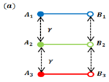
There has been a growing interest in the study of the tunneling problem of charge carriers in trilayer graphene systems including ABA- and ABC-stacked trilayer graphene (TLG) [18, 19]. In the present work, we consider the AAA-stacked TLG as schematically shown in Figure 1(a), which is composed of three single layers, each sublattice in a top layer is located directly above the same one in the bottom layer. The unit cell of an AAA-stacked consists of 6 inequivalent carbon atoms with two atoms for each layer. We study the electronic transport through np and npn junctions for AAA-stacked TLG where two kinds of gates will be considered such that the first causes an equal potential shift for all three layers and the second induces an interlayer potential difference between neighboring layers. We show that the quasiparticles in AAA-stacked TLG are not only chiral but also labeled by an additional cone index . We obtain band structures that are composed of three Dirac cones and depending on the cone indexes and the chirality indexes. Our theoretical model is based on the well established tight binding Hamiltonian [29]. The single and double gates act as a boundary for which we calculate the three transmission probabilities as function of the angle of incidence and Fermi energy of the incident electron for different configurations of the devices. Subsequently, we numerically evaluate the total conductance and underline the basic features of our system.
The rest of the paper is organized as follows. In section 2, we formulate our model by setting the Hamiltonian system used to describe AAA-stacked TLG. We explore the mirror reflection symmetry of the lattice in the plane of its central layer to determine the solutions of the energy spectrum in each layer (). Later on, we present the formalism, indicate the different propagating modes, define the four different cases for transmission for the six-band model and explain only the three possible transmission probabilities. In section 3, using the transfer matrix at boundaries together with the incident, transmitted and reflected currents we end up with three transmission probabilities. Next, we numerically discuss the obtained transmissions for each individual cones () for np and npn junctions to underline the behavior of our system. In section 4, we show the numerical results for the conductance and investigate the contribution of each transmission channel. Finally, we conclude our work and emphasize our main results.
2 Tight binding formalism
We consider a system consisting of three layers of graphene having the AAA-stacking structure. The unit cell consists of six atoms labeled , in the top layer, , in the central layer and , in the bottom layer as depicted in Figure 1(a). Each carbon atom of the bottom (center) layer is located above the corresponding atom of the center (top) layer, respectively and they are bound by an interlayer coupling energy . For the considered system, we define two different potential profiles where the first causes a potential shift equal for all three layers and the second one induces an interlayer potential difference between neighboring layers.
The Dirac fermions are scattered by an np junction and an npn junction along the x-direction. Therefore, the charge carriers in AAA-stacked trilayer is described by the following six-band Hamiltonian
| (1) |
The eigenstates of are the six component spinors , where are the envelope functions associated with the probability amplitudes of the wave functions on the and sublattices of the three layers. In (1), is a vector of Pauli matrices, is the Fermi velocity in monolayer graphene, is the momentum, is a general potential term, corresponds to an externally induced interlayer potential difference and describes the interlayer hopping parameter. Exploiting mirror reflection symmetric of the lattice in the plane of its central layer, we perform a unitary transformation to a basis of the spinor components by combining the atomic wave functions with and with . This operation transforms to , where , and .
With this, the Hamiltonian (1) is transformed into
| (2) |
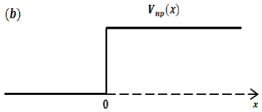
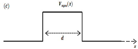
The above form of the Hamiltonian consists of a monolayer-like (bottom, right) and a bilayer-like (top, left) blocks that are connected by the parts responsible for the interlayer potential difference . The two blocks result in a superimposed linear from the monolayer and bilayer spectrum near the Dirac point as shown in 2. In that case, electrons propagating in AAA-stacked TLG can propagate through two different modes, one monolayer-like and one AA-stacked bilayer-like mode. As long as the mirror symmetry remains intact, both modes will not interact and scattering between them is prohibited. Here we shall study the problem of the tunneling of electron through a np junction (Figure 1(b)) and npn junction (Figure 1(c))
| (3) |
where is the height of the potential, which corresponds to the single gate term, and the parameter describes the effect of a double gate. The potential is for the center layer and for the top and bottom layers.
To proceed further, let us set the length scale as well as employ the dimensionless quantities to simplify the notation such that the energy terms can be parameterized by interlayer coupling , then , , , and . The system is infinite along the y-direction so that and hence we can write . The Hamiltonian (2) used together with the spinor in the eigenvalue equation to get six linear differential equations of the from
| (4a) | |||
| (4b) | |||
| (4c) | |||
| (4d) | |||
| (4e) | |||
| (4f) | |||
Combining the above equations by eliminating the unknowns one at time to end up with the second order differential equation
| (5) |
where the wave vectors along the x-direction are defined by
| (6) |
This form of the wave vectors consists of monolayer-like () and AA-stacked bilayer-like (), where is the cone index such that for the center cone and () for the bottom (top) cone. The energy bands corresponding to the wave vectors read as
| (7) |
The energy eigenvalues outside the barrier are then given by
| (8) |
Here and are the chirality indexes of a quasiparticle in the barrier and outside the barrier regions, respectively. Here (or ) and (or ) for electron-like and hole-like particles, respectively. The wave vector corresponding to this energy band is given by .
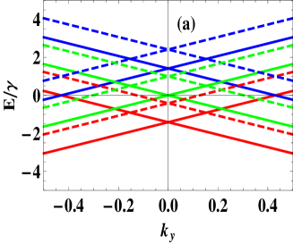
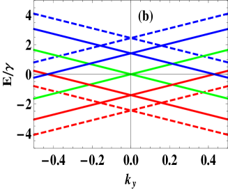
Plot of the energy bands inside and outside the barrier regions, as defined in (7) and (8), as a function of the momentum are shown in Figure 2. In this Figure, (red line) correspond to the bottom cone, (green line) for the center cone and (blue line) for the top cone. Whereas, the energy bands, for , of the AAA-stacked trilayer graphene are linear and just like three copies of the monolayer band structure, where the two bands () are shifted up and down by (see Figure 2(a)). We notice that the existence of three Dirac points located at , with , and two among them () are shifted either by or by . In addition, by increasing the potential height , the energy bands are shifted upwards also by . To see the effect of the interlayer potential difference , we plot the energy bands for and in Figure 2(b). When , one of the two Dirac points () is shifted by and the other by , while the third one () remained in the same position. The effect of can also be taken into account by a renormalization of the interlayer hopping energy of AAA-stacked trilayer graphene, , to a new interlayer potential difference dependent hopping energy, .
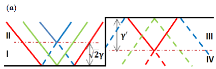
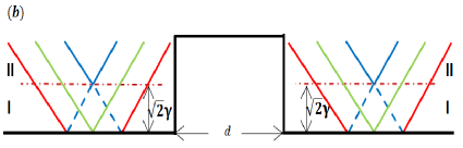
Figure 3 presents the band structure of AAA-stacked trilayer for single and double gates. In the incident region, the electron states can be subdivided into two regimes. The first one (I) () where the electron is hole-like particle, while where the electrons are electron-like particle. The second one (II) () where for the electrons are electron-like. However, inside the barrier region, the holes can also have two chiralities as denoted by regimes (III) and (IV). Note that we have nine transmissions that are related to the band structures in the np or npn junctions. In addition, we notice that for the intra-cone transitions (i.e. processes), there exist four cases for transitions across the np junction (Figure 3 (a)): (1) electron in regime I hole in regime III, (2) electron in regime I hole in regime IV, (3) electron in regime II hole in regime III, and (4) electron in regime II hole in regime IV. For the npn junction (Figure 3 (b)): (1) electron in regime I electron in regime I, (2) electron in regime I electron in regime II, (3) electron in regime II electron in regime I, and (4) electron in regime II electron in regime II. However, all inter-cone transitions (i.e. processes) are strictly forbidden due to the orthogonality of electron wave functions with a different cone indexes [30]. As already mentioned above, the transitions depend on the incident and transmission regions, so they depend on the presence or absence of the band gap induced by the single or double gates. For each of the four transitions cases the transmission can be calculated using the same method. The cone index is introduced while the chirality of the massless Dirac quasiparticles is not necessarily conserved during a transition state [30].
3 Transmission probabilities
Next we shall show in detail the calculation of the transmission probabilities. The transfer-matrix method together with appropriate boundary conditions was implemented for electrons across the np and npn junctions in our system. We notice that for AAA-stacked trilayer graphene, in the six band model, we have six reflection and six transmission channels [18]. Since, for AAA-stacked trilayer graphene, all inter-cone transitions () are strictly forbidden, then only three transmissions () are possible, one of monolayer-like and the two others of bilayer-like. Thus, we can reduce the six-band model to the following two-band model of monolayer-like () and four-band model of AA-stacked bilayer-like (). The plane-wave solutions for the Schrödinger equation can be represented by
| (9) |
where and are defined by
| (12) |
| (17) |
The index denotes each potential region, for the incident region, for the potential barrier region and for the transmission region, are the phase, and are defined by and . We are interested in the normalization coefficients, the components of and , on both sides of the np and npn junction structure. In other words in the incident region we have and and in the transmission region we have and , where and are the reflection and transmission coefficients of each cone (), respectively.
We need to match the wave functions at the boundaries between different regions. This procedure is most conveniently expressed in the transfer matrix formalism [31]. After a straightforward algebra we get the transfer matrix for np and npn junctions
| (21) | |||||
Here is determined by (12) and (17) at . Consequently, we have three channels for the transmission probability in each individual cone () for np and npn junctions.
3.1 np junction
The transmission probabilities for the intracone transitions with different cone index (i.e. processes) is zero [30]. This can be understood by considering the step potential as a sharp perturbation. While for the intercone transitions with the same cone index (i.e. processes) we have three transitions given by
| (22) | |||
| (23) | |||
| (24) |
where and are the elements of the transfer matrix given above.
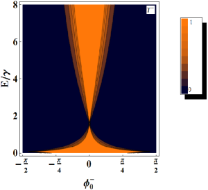
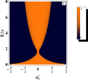
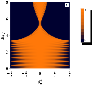
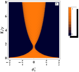
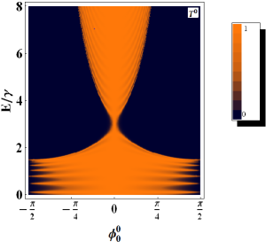
We first consider the case of np junction with . In Figure 4, we present the contour plot of the three transmissions: one of monolayer-like () and two of AA-stacked bilayer-like (), as a function of the incident angle and its energy, with physical parameters and . We can clearly see that the three transmission () exhibits a maximum (perfect transmission) for [30] and for normal incidence , as predicted [32] and observed experimentally [33, 34]. The major difference between the monolayer-like () and AA-stacked bilayer-like () is that the monolayer-like is only described by pseudospin, while the bilayer-like is described by an additional cone index, i.e. . In addition, the chirality of electron in the incident region () is always , while for the hole in transmission region it can be . For we have the usual refraction and for the electron transmission is equivalent to the optical case of negative refraction. We recall that for AA-stacked bilayer-like () the band structure is composed of two Dirac cones shifted by , one can clearly see that the transmission for both cones (), has the same form as that in the case of monolayer-like (). We observe also that the three transmissions curves () are symmetrical with respect to the normal incidence and the three Dirac points are located at , with .
3.2 npn junction
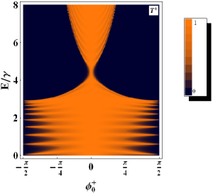
Now, we use (21) to explore the electronic transport properties through an npn junction based on the AAA-stacked trilayer graphene. The three transmissions are defined by
| (25) | |||
| (26) | |||
| (27) |

In the following calculation, we start with an npn junction in the
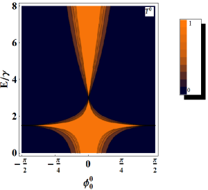
absence of double gates. In Figure 5, we show the
density plot of the three transmissions () as a function
of the incident angle () and its energy for both cones
with physical parameters: , , and
. The different colors from blue to orange correspond to
different values of the transmission from 0 to 1. It is important
to note that in the case of AAA-stacked trilayer graphene the band
structure is composed of three copies of the monolayer band
structure [35]. One of them () is shifted
by and the other () by ,
while the third one () remains in the center.
Then we end up with three Dirac points located at , with . For the transmission
of the center layer the Dirac points correspond to ,
for the top layer correspond to and the
bottom layer correspond to .
In the case of AA-stacked bilayer-like, for both cones
(), it has the same form as that in the case of
monolayer-like (). However, for AA-stacked bilayer-like graphene both the electrons
and holes have the same chirality index while in the
case of monolayer-like graphene the electron has always and
for the hole. We can see from that there is
a perfect transmission for normal or near normal incidence
(), which is a manifestation of the Klein
tunneling [32]. These results were also found in the
case of monolayer graphene and AA-stacked bilayer graphene.
Moreover, we find that the single gate () behavior in
AAA-stacked trilayer graphene is a superposition of monolayer-like
and bilayer-like systems, which are similar to those
obtained for ABA-stacked trilayer graphene [18].
Now, we will turn to the discussions of the influence of the interlayer potential difference on the three transmissions . We show the density plot of the three transmissions as function of the incident angle and its energy in Figure 6 with , and . We notice that two Dirac points () are shifted by and the other by and the third one remains in the same position (see Figure 5). These cases do not exist in the AA-stacked bilayer graphene [30], but in the presence of we have a transmission gap around the Dirac point. As already mentioned above, we have perfect transmission, which is a manifestation of Klein tunneling effect. However, in the case of AAA-stacked trilayer graphene, the effects of can be taken into account by a renormalization of the interlayer hopping energy, , to a new interlayer potential difference dependent hopping energy, . We notice that in the case AA-stacked bilayer graphene[30], for , the Klein tunneling effect is suppressed. Also, we find that the single and double gate behavior in the case of AAA-stacked trilayer graphene is a superposition of monolayer-like and bilayer-like systems. This is not the case for ABA-stacked trilayer graphene, where the double gate mixes both types of bands and breaks the angular symmetry with respect to normal incidence [18].
4 Conductance
The conductance through junction can be expressed in terms of the transmission probabilities established before. We will see how the three conductance of each cone channel () will behave. For this purpose, we evaluate by using the Landauer-Büttiker formula [36]
| (28) |
where the unit conductance is given by
| (29) |
and the factor is due to the spin and valley degeneracy, is the width of the sample in the -direction and
| (30) |
The total conductance is defined as the sum of the conductance channels in each individual cone such as
| (31) |
where the factor is required since the total conductance is
a contribution of three cones. Whereas, in the case of AA-stacked
bilayer graphene, there are two transmissions channels then the
total conductance is the sum of two conductances channels with a
factor of [30]. In the forthcoming analysis, we
evaluate numerically the conductance in AAA-stacked bilayer
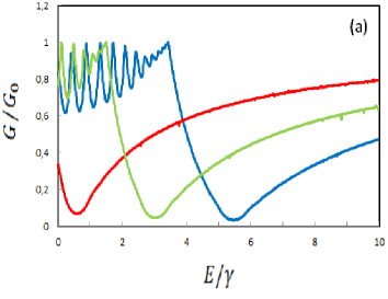
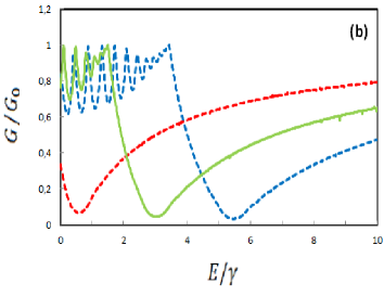
graphene. In Figure 7 we show the three
conductance through a single barrier structure ( junction) in
each individual cone as a function of the energy for
and . In Figure 7(a) the conductances
are plotted for while in Figure
7(b) for . It is important to
note that in the case of AAA-stacked trilayer graphene, in Figure
7(a), we have the three conductances for each
individual cone ().
One of them () is shifted by and the other
() by , while the third one ()
remains in the center. Then we end up with three Dirac points
located at , with (). For
energies smaller than , the conductance of the
single barrier presents peaks.
While for , the conductance increases and the
peaks are absents. To see the effect of the externally induced
interlayer potential difference , we plot the three
conductances as function of the energy in Figures
7(b). We note that two Dirac points for
and are shifted by
and the
other by . Moreover, the third Dirac point for
remains in the same position.
5 Conclusion
We have investigated the electronic transport properties through np and npn junctions based on the AAA-stacked trilayer graphene. The Hamiltonian model describing the system under consideration allowed us to determine the solutions of the energy spectrum. The obtained bands are composed of three Dirac cones that depend on the cone and chirality indexes. For AAA-stacked trilayer graphene, we have shown that the transmission in the inter-cone transition ( processes) is strictly forbidden due to the orthogonality of electron wave functions, in contrast of the ABA- and ABC-stacked trilayer graphene cases. In addition, our results showed that there are three transmission probabilities for each individual cone (), one of monolayer-like and two of AA-stacked bilayer-like . The quasiparticles in AAA-stacked trilayer graphene are not only chiral but also labeled by an additional cone index . It was noticed that is a strictly conserved quantity while the chirality index is not necessarily conserved during a state transition.
Subsequently, we have numerically investigated the obtained three transmission probabilities for each individual cone. For np junction with single gate, we have perfect transmission for and for normal incidence . In addition, we have found that the three transmissions have the same form as those found in the case of monolayer graphene. We have shown that there are three Dirac points located at where . Also, we have found that the single and double gated behavior are a superposition of monolayer-like and bilayer-like systems. These results are similar to ABA-stacked trilayer graphene for a single gate. However, double gated mixes both types of bands in the case of ABA-stacked trilayer graphene. Furthermore, we have studied the influence of the double gated on the three transmission for single barrier structure and shown that it can be taken into account by a renormalization of the interlayer hopping energy to a new interlayer potential .
Based on the obtained results for the transmission probabilities we have found three conductances channels through junction. For , that there are three Dirac points located at with . Also, we have investigated the effect of the interlayer potential difference on the conductance channel in each cone. It was noticed that the two Dirac point for and are shifted by and the other by . Moreover, the third Dirac point for remains in the same position. Finally the total conductance is analyzed as the average of the three conductances channels in each cone.
Acknowledgments
The generous support provided by the Saudi Center for Theoretical Physics (SCTP) is highly appreciated by all authors. AH and HB acknowledge the support of King Fahd University of Petroleum and minerals under research group project RG1502-1 and Rg1502-2.
References
- [1] K. S. Novoselov, A. K. Geim, S. V. Morozov, D. Jiang, Y. Zhang, S. V. Dubonos, I. V. Grigorieva, and A. A. Firsov, Science 306, 666 (2004).
- [2] K. S. Novoselov, A. K. Geim, S. V. Morozov, D. Jiang, M. I. Katsnelson, I. V. Grigorieva, S. V. Dubonos, and A. A. Firsov, Nature 438, 197 (2005).
- [3] Y. B. Zhang, Y. W. Tan, H. L. Störmer, and P. Kim, Nature 438, 201 (2005).
- [4] C. Berger et al., J. Phys. Chem. B 108, 19912 (2004).
- [5] J. S. Bunch, Y. Yaish, M. Brink, K. Bolotin, and P. L. McEuen, Nano Lett. 5, 2887 (2005).
- [6] K. S. Novoselov, D. Jiang, F. Schedin, T. J. Booth, V. V. Khotkevich, S. V. Morozov, and A. K. Geim, Proc. Nat. Acad. Sc. 102, 10451 (2005).
- [7] K. S. Novoselov, E. McCann, S. V. Morozov, V. I. Fal’ko, M. I. Katsnelson, U. Zeitler, D. Jiang, F. Schedin, and A. K. Geim, Nature Physics 2, 177 (2006).
- [8] S. V. Morozov, K. S. Novoselov, F. Schedin, D. Jiang, A. A. Firsov, and A. K. Geim, Phys. Rev. B 72, 201401 (2005).
- [9] B. Partoens, and F. M. Peeters, Phys. Rev. B 75, 193402 (2007).
- [10] M. Koshino, and T. Ando, Phys. Rev. B 77, 115313 (2008).
- [11] J. Nilsson, A. H. Castro Neto, F. Guinea, and N. M. R. Peres, Phys. Rev. B 78, 0454005 (2008).
- [12] A. A. Avetisyan, B. Partoens, and F. M. Peeters, Phys. Rev. B 80, 195401 (2009).
- [13] M. Koshino, Phys. Rev. B 81, 125304 (2010).
- [14] S. Das Sarma, S. Adam, E. H. Hwang, and E. Rossi, Rev. Mod. Phys. 83, 407 (2011).
- [15] J. Jung, F. Zhang, Z. Qiao, and A. H. MacDonald, Phys. Rev. B 84, 075418 (2011).
- [16] P. L. De Andres, F. Guinea, and M. I. Katsnelson, Phys. Rev. B 86, 245409 (2012).
- [17] W. A. Munoz, L. Covaci, and F. M. Peeters, Phys. Rev. B 88, 214502 (2013).
- [18] B. Van Duppen, S. H. R. Sena, and F. M. Peeters, Phys. Rev. B 87, 195439 (2013).
- [19] B. Van Duppen, and F.M. Peeters, Europhys. Lett. 102, 27001 (2013)
- [20] S. Bala Kumar, and J. Guo, Appl. Phys. Lett. 100, 163102 (2012).
- [21] B. Van Duppen, and F. M. Peeters, Appl. Phys. Lett. 101, 226101 (2012).
- [22] R. Quhe, J. Zheng, G. Luo, Q. Liu, R. Qin, J. Zhou, D. Yu, S. Nagase, W.-N. Mei, Z. Gao and J. Lu, NPG Asia Mater. 4, (2012) e6.
- [23] C. J. Tabert and E. J. Nicol, Phys. Rev. B 86, 075439 (2012).
- [24] T. Ando, J. Phys. Conf. Ser. 302, 012015 (2011).
- [25] Y.-F. Hsu, and G.-Y. Guo, Phys. Rev. B 82, 165404 (2011).
- [26] E. Prada, P. San-Jose, L. Brey, and H. Fertig, Solid State Commun. 151, 1075 (2011).
- [27] L. Brey, and H. A. Fertig, Phys. Rev. B 87, 115411 (2013).
- [28] Y. Mohammadi, R. Moradian, Physica B 442, 66 (2014).
- [29] Y. Mohammadi, R. Moradian, and F. S. Tabar, Solid State Commun. 193, 1 (2014).
- [30] M. Sanderson, Y. S. Ang, and C. Zhang, Physical Review B 88, 245404 (2013).
- [31] L.-G. Wang and S.-Y. Zhu, Phys. Rev. B 81, 205444 (2010).
- [32] M. I. Katsnelson, K. S. Novoselov and A. K. Geim, Nat. Phys. 2, 9 (2006).
- [33] A. F. Young and P. Kim, Nat. Phys. 5, 222 (2009).
- [34] N. Stander, B. Huard and D. Goldhaber-Gordon, Phys. Rev. Lett. 102, 026807 (2009).
- [35] X. Chen, J.-W. Tao and Y. Ban, Eur. Phys. J. B 79, 203 (2011).
- [36] Ya. M. Blanter and M. Büttiker, Physics Reports 336, 1 (2000).