Effect of hexagonal patterned arrays and defect geometry on the critical current of superconducting films
Abstract
Understanding the effect of pinning on the vortex dynamics in superconductors is a key factor towards controlling critical current values. Large-scale simulations of vortex dynamics can provide a rational approach to achieve this goal. Here, we use the time-dependent Ginzburg-Landau equations to study thin superconducting films with artificially created pinning centers arranged periodically in hexagonal lattices. We calculate the critical current density for various geometries of the pinning centers — varying their size, strength, and density. Furthermore, we shed light upon the influence of pattern distortion on the magnetic-field-dependent critical current. We compare our result directly with available experimental measurements on patterned molybdenum-germanium films, obtaining good agreement. Our results give important systematic insights into the mechanisms of pinning in these artificial pinning landscapes and open a path for tailoring superconducting films with desired critical current behavior.
pacs:
74.20.De, 74.25.Sv, 74.25.Wx, 05.10.aI Introduction
Superconducting films are exemplary systems to study the effect of different pinning landscapes on the resulting critical current of the system. In general, pinning centers reduce the mobility of magnetic vortices and, as a result, their dissipative effects.Blatter et al. (1994); Nattermann and Scheidl (2000); Blatter and Geshkenbein (2003) Experimentally, defects can be introduced into superconducting films in a controllable fashion using advanced nanofabrication techniques such as focus ion beam (FIB) milling,Latimer et al. (2013) electron beam lithography (EBL),Kemmler et al. (2006) EBL combined with reactive ion etching,Wang et al. (2013, 2016) or ion irradiation.Trastoy et al. (2014) Many artificial pinning array structures (pinscapes) have been studied experimentally as well as numerically, for example, square arrays of antidots,Baert et al. (1995); Harada et al. (1996); Moshchalkov et al. (1998); Berdiyorov et al. (2006a, b, c, 2007); Sabatino et al. (2010); Silhanek et al. (2010); Wang et al. (2016) hexagonal (or triangular) pinning lattices,Kemmler et al. (2009); Rablen et al. (2011) honeycomb arrays,Wu et al. (2005); Reichhardt and Olson Reichhardt (2007, 2008); Latimer et al. (2012) Penrose lattice arrays,Misko et al. (2005, 2006, 2010); Kramer et al. (2009); Silhanek et al. (2006); Misko and Nori (2012); Rablen et al. (2011) blind hole arrays,Bezryadin et al. (1996); Raedts et al. (2004); Berdiyorov et al. (2009) diluted periodic arrays,Guénon et al. (2013); Kemmler et al. (2009) composite lattices,Silhanek et al. (2005) pinscapes with density gradients,Wu et al. (2007); Motta et al. (2013); Wang et al. (2013); Guénon et al. (2013); Misko and Nori (2012); Ray et al. (2013, 2014); Wang et al. (2016) and pinscapes with geometrically frustrated energy landscape.Libál et al. (2009); Latimer et al. (2013); Trastoy et al. (2014) These studies were limited to either small sizes, two-dimensional systems, and/or one particular configuration.
In the present work, we perform a systematic study of various hexagonal pinning lattices using large-scale simulations of the time-dependent Ginzburg-Landau (TDGL) equations. This method can capture the vortex dynamics in a realistic way and is the best compromise between microscopic simulations and describing the phenomenological behavior of a superconducting material using currently available supercomputers.Sadovskyy et al. (2016a); Koshelev et al. (2016) Within the TDGL approach, the collective dynamics of vortices in thin, but finite-thickness, superconducting films are taken into account automatically and allow us to obtain results on experimentally relevant length scales. We vary the size, strength, and density of the pinning sides and study the underlying vortex dynamics, which explains the magnetic-field-dependent critical current.
Naively, one can expect to find simple matching effects for the field-dependent critical current, e.g., peaks at field values corresponding to vortex numbers, which are integer multiples of the number of pinning sites (and minor peaks at simple fractions). However, in reality, vortex dynamics and pinning are much more diverse, such that this theoretical picture is not (always) observed. For example, vortices are not only confined to the pinning centers, but also can be caged in between them due to repulsion at certain filling fractions, depending on the geometry of the pinscape.
A second main aspect of this work is to study the influence of distortions on the periodic pinning array, i.e., the question on how matching effects can be destroyed.
Finally, we compare our numerical results with experimental data on artificially patterned molybdenum-germanium (MoGe) films to explain the vortex behavior of these systems by large-scale simulations. This represents another aspect of the critical-current-by-design paradigm.Sadovskyy et al. (2016b)
The article is organized as follows. We introduce the numerical description in Secs. II.1–II.3 and the experimental technique in Sec. II.4. The comparison between numerical and experimental results is presented in Sec. III.1. The dependence on inclusion strength is discussed in Sec. III.2 and the influence of distortions of the periodic pinning arrays is discussed in Sec. III.3. We summarize our results in Sec. IV.

II Model and Experiments
Here we introduce our model of artificially patterned superconducting films and explain the experimental setup and fabrication of the samples, which we compare with the numerical results.
II.1 Simulations of patterned superconducting films
In order to model the superconducting films, we use the TDGL equation and apply it to systems with periodically modulated defects.
The TDGL equations effectively capture the collective vortex dynamics and pinning in realistic systems. As the London penetration depth is typically large compared to the coherence length in superconducting films, the TDGL equations can be simplified to just the time evolution of the superconducting order parameter, , with a constant magnetic field perpendicular to the film, i.e.Sadovskyy et al. (2015),
| (1) |
where is the scalar potential, is the vector potential associated with the external magnetic field, and is an additive thermal-noise term. This equation provides an adequate, quantitative description of strong type-II superconductors in the vortex phase. Equation (1) is written in dimensionless units, where the unit of length is the superconducting coherence length , the unit of time is , is the London penetration depth, is the normal-state conductance, and the unit of the magnetic field is given by the upper critical field ( is the electron’s charge and is the speed of light).
Thermal fluctuations, described by , are determined by its time and space correlations and absolute temperature.Sadovskyy et al. (2015) Since we are targeting low temperature vortex behavior, this term becomes negligible. For comparison, the typical temperature is K in the experiment on MoGe films (see below).
We model the superconducting film as a thin slab with finite thickness. In order to capture the relevant collective vortex dynamics in the system, we simulate a sample of size , where we used the coherence length nm of MoGe for the physical dimensions. This sample is spatially discretized on a regular mesh with grid points with quasiperiodic boundary conditions in (along the applied current) and directions, and open boundary condition in the direction (along the magnetic field). The thickness of nm corresponds to the actual experimental film, but its lateral dimensions are about four times smaller than the actual film size, but are sufficient to capture “bulk” properties correctly.
II.2 Modeling of inherent and artificial defects
We model material defects in the Ginzburg-Landau formalism using so-called pinning, where the critical temperature is spatially modulated due to defects that cause pair-breaking scattering.Kwok et al. (2016); Berdiyorov et al. (2012a, b) We use the dimensionless coefficient of the linear term in Eq. (1), , to introduce spatial modulations. This means that for , the linear coefficient is negative, which models normal defects, while for and different from the bulk , weak superconducting defects are captured. We use this modulation to both model the inherent defects of the material as well as the larger-scale artificial periodic pinning array. Our equation is scaled such that for the bulk superconductor (due to the choice of the length scale), i.e., , where is the critical temperature inside the inclusions and is the bulk critical temperature. The pinning centers of the array are modeled by short cylinders of diameter and height . Together with the value of , these are the parameters controlling the pinning properties of the defects.
Since even the pristine material (without pinning array) typically has a finite critical current, some mechanism of pinning has to be present. In the case of amorphous MoGe films, there are several possible vortex pinning candidates. While these films are typically very flat and homogeneous, they still have some small surface roughness (of the order of a few nanometers) and spatial composition variations. However, it is not known which type of defects causes the inherent pinning. Nevertheless, we need to take these weak pinning centers into account to obtain a finite critical current for the simulated pristine sample. We chose different types of modulations in order to match the simulated critical currents with that of the experimental sample without periodic pinning array to obtain a baseline for the pristine sample. For all studied cases — weak random modulation near everywhere, small polycrystalline Voronoi patterns with typical size of a few coherence length, or isolated small spherical inclusions — we could fit the pristine field dependence of the critical current. We therefore chose, throughout this work, to model the inherent inhomogeneities of MoGe by small randomly placed background inclusions of diameter nm with (i.e., K) occupying 1.8% of the sample volume.
In contrast to layered high- materials, MoGe films have no large-scale defects due to the anisotropy of the material, which we therefore did not include in our model.
II.3 Critical current calculation
In order to obtain the critical current density from the simulations, we apply a current to the system along the direction. The total (normal and superconducting) in-plane current density is then given by the expression
| (2) |
in units of . For an applied current density , we need to solve an additional ordinary differential equation for the voltage: , where is the spatial average over the complete system. (The maximum theoretical depairing current density is .) In this case, we also need to take into account the condition , resulting in the Poisson equation,
| (3) |
for the scalar potential in addition to Eq. (1).
In order to determine the critical current value , we dynamically adjust the external current in the simulation such that the electric field or voltage drop across the sample has a predefined value. Choosing this electrical field sufficiently small, and averaging the current density over different background defect configurations and time, we obtain the critical current density , where and is the average over realizations and time, respectively. Here, we use the finite electric field criterion to determine the critical current, where is the electric field unit. Note that the value used in the numerical simulations is much higher than the level of dissipation corresponding to the value of V/cm, routinely used as a practical criterion for in experiments. Therefore, the simulated critical currents are expected to be somewhat higher than the experimental ones, but due to the large exponent of the - curve near the transition, there is no qualitative difference expected.
We average the dynamically adjusted current over Ginzburg-Landau time steps and over different realizations of the initial conditions of the order parameter and random background inclusions. This method gives the same result (within 2% accuracy) as calculating the current-voltage characteristics at many different applied currents and defining from in the - curve.Sadovskyy et al. (2016a, b)
II.4 MoGe sample and patterning technique
Since we compare experimental results on Mo0.79Ge0.21 films with our simulations, we briefly characterize these samples here. The 50-nm-thick MoGe films were divided into sections using photolithography and magnetron sputtering deposition. The resulting sample has a critical temperature of K, while transport (-) measurements were carried out at temperature K. We estimate the coherence length in this sample to be nm, with an upper critical field of G, and depairing current density MA/cm2 using typical material parameters for MoGe. The hexagonal array of pinning centers of diameter nm and lattice constant nm was patterned using an EBL patterned nanohole mask and reactive ion etching technique, shown in Fig. 1a.
A representation of the modulation in the simulation for this sample is shown in Fig. 1b, where the defects have a diameter of and and the lattice constant of (in dimensionless units).
III Results
III.1 Simulations vs experiments
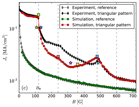
Figure 1c demonstrates the comparison between the experimental and numerical dependence. As mentioned before, we add a small spherical background defect to the clean simulation system with diameter nm, occupying 1.8% of the sample volume, in order to reproduce the experimental reference curve (gray diamonds) of the pristine sample. The resulting numerical dependence averaged over 16 realizations of disorder is shown by green circles and nicely coincides with the experimental reference curve shown by gray diamonds.
The red curve in Fig. 1c demonstrates the simulated dependence in the presence of a hexagonal lattice of patterned defects. For the simulations, the diameter of the holes is nm and the lattice constant is nm, mimicking the experiment. We chose the depth of the inclusions to be nm and the critical temperature inside the inclusions as . The resulting simulated curve coincides well with the experimental one at fields lower than and higher than . Field values that are integer multiples of the matching field G [the field generating a single vortex per inclusion or per lattice unit-cell area ] are shown by vertical dashed lines. For , the simulations show somewhat smaller critical currents compared to the experiment. However, simulations reproduce almost all of the qualitative features of the curve such as the minimum at and maximum at . At , we see a down kink resulting from the vortex caging effect, where an additional vortex is pinned in the center of a hexagonal vortex lattice cell by repulsive forces from vortices that reside in the inclusions.Berdiyorov et al. (2006b)
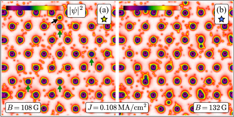
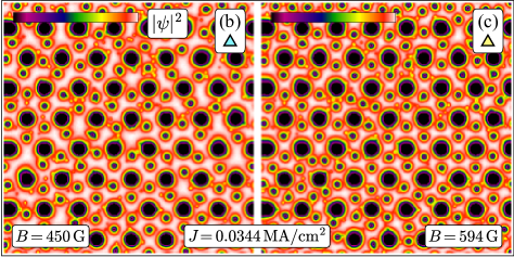
Next, we compare the vortex dynamics near the drop at . Snapshots of the order parameter amplitude are shown in Fig. 2a for G and Fig. 2b for G; these values are marked by yellow and blue stars in Fig. 1c, accordingly. (The corresponding vortex dynamics can be seen in the supplementary video.) The external current is the same for both snapshots and chosen to be . In these density plots, which are cross sections at fixed nm, an amplitude of or “full” superconductivity corresponds to white regions, while the order parameter is completely suppressed in black areas with . Since the chosen cross section is slightly underneath the inclusion cylinder pieces, they appear violet with due to the proximity effect. Since the order parameter is completely suppressed in the vortex cores, they appear black; thus one can distinguish occupied and unoccupied inclusions. Figure 2a with and shows four unoccupied inclusions and one “caged” vortex pinned by repulsive forces at the center of the triangular cell. In Fig. 2a with and , all of the inclusions pin one vortex and five nearly free vortices drift between the inclusions and produce a finite voltage across the sample.
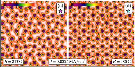
With increasing magnetic field, the number of vortices in between and on the pinning site increases. At a fixed applied current, we compare the order parameter amplitude for two values of the magnetic field, G and G, shown in Figs. 2c and 2d, respectively. (See also the supplementary video showing the vortex dynamics.) The external current is . The corresponding current and magnetic field values are marked by magenta and cyan crosses in the - diagram; see Fig. 1c. For these two parameter sets, the vortex matter behavior is quite different from Figs. 2a and 2b. Indeed, in Fig. 2c with , inclusions pin one or two vortices, but “caged” vortices can “squeeze” between the inclusions generating dissipation. In Fig. 2d with , almost all inclusions pin two vortices each and caged vortices form a honeycomb lattice.
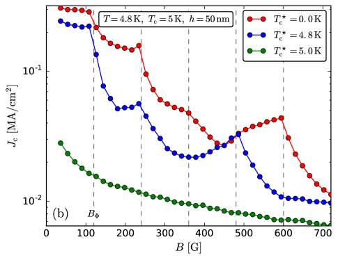
In this regime, the repulsion between vortices at inclusions and caged vortices is so strong that the latter cannot squeeze through the hexagonal pattern of inclusions and, consequently, results in the peak at . The vortex lattice structure at this field, corresponding to four times the matching field, is defined by two vortices per inclusion () and a hexagonal lattice in between them (). This is a typical scenario: if one can associate two caged vortices to one inclusion and the inclusion pins vortices, one observes a peak at the -th matching field, . For , each inclusion pins one vortex and cages two (see, e.g., blue curve in Fig. 6a below); for each inclusion pins two vortices (red curve in Fig. 1c); and for , three vortices are pinned by an inclusion (blue curve in Fig. 5a below). Peaks appearing at or can be related to single or double occupation of pinning centers.
Before the -th peak (), at the preceding -th matching magnetic field, , the critical current has a smaller value, . In this regime, one caged vortex per inclusion is missing. These vacancies can be easily occupied by neighboring caged vortices and therefore allow vortices to move one by one by the Lorentz force. This mechanism significantly reduces the critical current at the -th matching magnetic field and is more pronounced for stronger pinning centers.
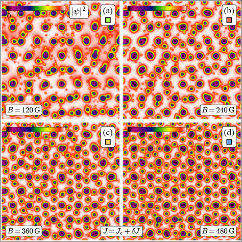
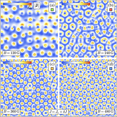
Figures 3 and 4 as well as the supplementary videos show snapshots of squared order parameter configurations and supercurrent for external current slightly above the critical current near the first four matching fields, with , illustrating the different pinning behavior and dynamics. (See video of dynamics of squared order parameter amplitude and supercurrent, combination of those, and combination with order parameter phase.) At the first matching field (120 G, one vortex per inclusion), vortices move mostly by jumping from one inclusion to another; see Fig. 3a. In contrast to that, near the second matching field, some doubly occupied defects lose one vortex, which then moves in between the defects; see Fig. 3b. At the two higher fields, Figs. 3c and 3d, vortices are also pinned in between the defects due to their repulsive interaction and defects have, at most, two pinned vortices in the stationary state. Above the third matching field, the vortex dynamics is still characterized by meandering motion in between the defects, while at the fourth matching field, they move via absorption and emission at the defects, which requires larger currents than for the second and third matching field. The higher value of the critical current at the fourth matching field is therefore a result of a “blocking” behavior of the vortices, which are pinned between inclusions.
III.2 Dependence on inclusion strength
Above we discussed a particular realization of the pinning array, which, at least qualitatively, explains the experimentally observed field dependence of the critical current. However, it is instructive to study the dependence of the overall behavior on the inclusion strength. In the framework of the chosen model, we can control the strength of the inclusions by changing the depth of the inclusions, the critical temperature inside the inclusions, and their diameter . All three quantities influence the pinning strength of the inclusions and one can expect that the effects from increasing are similar to the effects from decreasing .
Inclusion depth.
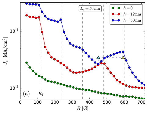
The curve for different inclusion depths of inclusions is shown in Fig. 5a. The green and red curves correspond to (reference) and nm (25% of the nm sample thickness). The same curves were compared to experiment in Fig. 1c. Surprisingly, the positions of the peaks in change with . Indeed, the blue curve in Fig. 5a for nm demonstrates two prominent peaks at and and has a local minimum near .
The difference between fully and partially drilled holes in the sample can be analyzed in the same way as in Sec. III.1. Snapshots of density plots are shown in Fig. 5b for G and Fig. 5c for G (magenta and cyan crosses in Fig. 5a); see also supplementary video of vortex dynamics. The external current is fixed at . The vortex dynamics is very similar to the one depicted in Figs. 2c and 2d. The only difference is that in Fig. 5b, each inclusion is stronger and pins three vortices. Therefore, the resulting vortex configuration gives rise to a peak at five times the matching field, having three vortices per inclusion and two caged vortices (as for nm) per pattern unit cell.
Critical temperature inside inclusion.
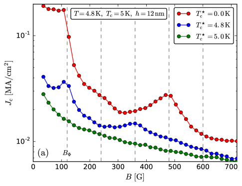
The dependence of the critical temperature inside the inclusion of depth nm is shown in Fig. 6a. Naturally, increasing reduces the pinning strength and therefore the critical current (compare the red curve for and blue curve for K). curves for inclusions penetrating the entire film, i.e., nm, are shown in Fig. 6b. As before, we see that increasing the pinning depth shifts the peak from (red curve in Fig. 6a) to (red curve in Fig. 6b). However, increasing the critical temperature inside the inclusions from to K moves the peak back to due to decreasing pinning strength of the inclusions (blue curve in Fig. 6b).
Dependence on inclusion diameter.
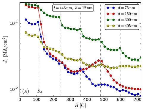
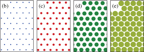
Figure 7a shows the dependences for different inclusion diameters. The corresponding hexagonal patterns are displayed in Figs. 7b–7e by the same colors. As one can see, the strength of the inclusions increases with their diameter until their volume fraction occupies too much of the sample. Indeed, pinning centers with relatively small diameter, nm, generate low critical current, as shown by the blue curve in Fig. 7a. These inclusions may pin one vortex only; thus we observe a peak at ( from pinned vortices and from caged vortices). For the increased diameter, nm, the peak shifts towards (red curve) as was discussed above.
The larger diameter, i.e., nm, creates a stronger pinning force resulting in higher (green curve in Fig. 7a). Concurrently, the larger pinning center may accommodate one to approximately eight vortices, depending on the applied magnetic field. This behavior is reflected by the series of peaks at each integer multiple of . In this regime, the system shows behavior similar to Josephson junction arrays frustrated by magnetic field. However, further increasing the inclusion diameter reduces (see yellow curve for nm). The main reason for the decrease in is the reduced superconductivity in the gaps between the inclusions, nm, which in turn reduces the effective potential barrier for hopping of vortices between inclusions. Additionally, large inclusion diameters simply decrease the effective superconductor cross section for supercurrent transport. One sees that the matching effects become much weaker in this case.
To summarize, we conclude that the vortex dynamics responsible for the critical current depends on two main factors: (i) matching field or hexagonal pattern constant and (ii) pinning strength of the inclusion. The latter depends on inclusion depth , critical temperature inside inclusion , and inclusion diameter . These three quantities are responsible for the pinning force of the inclusion and its ability to pin more than one vortex.
III.3 Influence of randomness
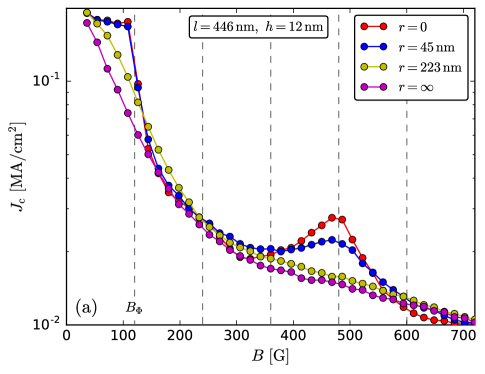
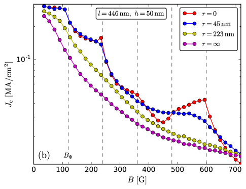
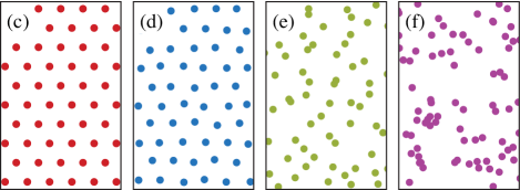
Finally, we discuss the influence of random displacements of the inclusions from their perfect lattice positions. This gives an insight on when matching effects become relevant and shows how possible lattice imperfections in experimental systems affect the vortex dynamics. Let us start with the perfect hexagonal lattice (Fig. 8c) and add some random displacement within an interval to the and positions of each inclusion. The resulting patterns are presented in Figs. 8d–8f. curves are shown in Fig. 8a for nm and in Fig. 8b for nm in corresponding colors.
The perfect hexagonal pattern (red lines in Figs. 8a and 8b), i.e., pattern with well-defined matching field , demonstrate the most nonmonotonic behavior with peaks at some integer multiples of as discussed before. With increasing randomness in the placement of the inclusions, , these peaks become less pronounced (blue). For some random placement, peaks or kinks near integer multiples of completely disappear (yellow) and, as a result, the curves become more monotonic. The values of the critical current for moderate randomness may be both lower or higher compared to the ordered pattern.
This order of defects is sometimes called hyperuniformity and is characterized by uniform defect placement on large scales and disordered placement on small scales. This hyperuniform order is characterized by higher critical current compared to uncorrelated defect placement (magenta). This result is in agreement with recent Langevin-dynamics analysis of pinning.Le Thien et al. (2016) In terms of critical current, there are two main differences between hyperuniform and uncorrelated patterns reducing in the latter: (i) the existence of large regions without pinning centers and (ii) clusters of the defects located too close to each other. Indeed, large regions of pure superconductor allow vortices to move freely. On the other hand, two defects located too close to each other might not produce a strong enough potential barrier preventing a vortex jumping from one defect to the other. A less important effect is the higher probability of overlapping defects for uncorrelated placement, which effectively lowers the number of pinning sites.
IV Conclusions
We carried out large scale time-dependent Ginzburg-Landau simulations of vortex dynamics in thin, hexagonally patterned superconducting films and reproduced experimentally measured critical currents in patterned MoGe thin-film samples. We studied the vortex dynamics inside the sample and revealed the underlying mechanisms for the critical current dependence on the magnetic field. In particular, we demonstrated how the position of peaks of the magnetic-field-dependent critical current is influenced by the depth and diameter of the individual defect, and we discussed the different types of vortex dynamics near these peaks. Overall, the field dependence of the critical current strongly depends on the defect morphology. Finally, we observed that spatial randomness in the position of inclusions smooths the critical current curve, i.e., increases or decreases it in certain value ranges. We found that a hyperuniform placement of inclusions can generate larger critical current than completely uncorrelated random pinscapes.
Acknowledgments.
We are delighted to thank A. E. Koshelev and G. Kimmel for illuminating discussions. The computational work was supported by the Scientific Discovery through Advanced Computing (SciDAC) program funded by the U. S. Department of Energy, Office of Science, Advanced Scientific Computing Research and Basic Energy Science. The computational part of this work was performed on Titan at the LCF at Oak Ridge National Laboratory (DOE Contract No. DE-AC05-00OR22725) and GAEA at Northern Illinois University. The experimental study at Argonne National Laboratory was supported by the U. S. Department of Energy, Office of Science, Basic Energy Sciences, Materials Sciences and Engineering Division. The nanopatterning and morphological analysis were performed at Argonne National Laboratory’s Center for Nanoscale Materials. Z. L. X. acknowledges NSF Grant No. DMR-1407175.
References
- Blatter et al. (1994) G. Blatter, M. V. Feigel’man, V. B. Geshkenbein, A. I. Larkin, and V. M. Vinokur, Vortices in high-temperature superconductors, Rev. Mod. Phys. 66, 1125 (1994).
- Nattermann and Scheidl (2000) T. Nattermann and S. Scheidl, Vortex-glass phases in type-II superconductors, Adv. Phys. 49, 607 (2000).
- Blatter and Geshkenbein (2003) G. Blatter and V. Geshkenbein, Vortex Matter, in The Physics of Superconductors, edited by K. Bennemann and J. Ketterson (Springer, Berlin Heidelberg, 2003) pp. 725–936.
- Latimer et al. (2013) M. L. Latimer, G. R. Berdiyorov, Z. L. Xiao, F. M. Peeters, and W. K. Kwok, Realization of artificial ice systems for magnetic vortices in a superconducting MoGe thin film with patterned nanostructures, Phys. Rev. Lett. 111, 067001 (2013).
- Kemmler et al. (2006) M. Kemmler, C. Gürlich, A. Sterck, H. Pöhler, M. Neuhaus, M. Siegel, R. Kleiner, and D. Koelle, Commensurability effects in superconducting Nb films with quasiperiodic pinning arrays, Phys. Rev. Lett. 97, 147003 (2006).
- Wang et al. (2013) Y. L. Wang, M. L. Latimer, Z. L. Xiao, R. Divan, L. E. Ocola, G. W. Crabtree, and W. K. Kwok, Enhancing the critical current of a superconducting film in a wide range of magnetic fields with a conformal array of nanoscale holes, Phys. Rev. B 87, 220501 (2013).
- Wang et al. (2016) Y. L. Wang, L. R. Thoutam, Z. L. Xiao, B. Shen, J. E. Pearson, R. Divan, L. E. Ocola, G. W. Crabtree, and W. K. Kwok, Enhancing superconducting critical current by randomness, Phys. Rev. B 93, 045111 (2016).
- Trastoy et al. (2014) J. Trastoy, M. Malnou, C. Ulysse, R. Bernard, N. Bergeal, G. Faini, J. Lesueur, J. Briatico, and J. E. Villegas, Freezing and thawing of artificial ice by thermal switching of geometric frustration in magnetic flux lattices, Nat. Nano 9, 710 (2014).
- Baert et al. (1995) M. Baert, V. V. Metlushko, R. Jonckheere, V. V. Moshchalkov, and Y. Bruynseraede, Composite flux-line lattices stabilized in superconducting films by a regular array of artificial defects, Phys. Rev. Lett. 74, 3269 (1995).
- Harada et al. (1996) K. Harada, O. Kamimura, H. Kasai, T. Matsuda, A. Tonomura, and V. V. Moshchalkov, Direct observation of vortex dynamics in superconducting films with regular arrays of defects, Science 274, 1167 (1996).
- Moshchalkov et al. (1998) V. V. Moshchalkov, M. Baert, V. V. Metlushko, E. Rosseel, M. J. Van Bael, K. Temst, Y. Bruynseraede, and R. Jonckheere, Pinning by an antidot lattice: The problem of the optimum antidot size, Phys. Rev. B 57, 3615 (1998).
- Berdiyorov et al. (2006a) G. R. Berdiyorov, M. V. Milošević, and F. M. Peeters, Novel commensurability effects in superconducting films with antidot arrays, Phys. Rev. Lett. 96, 207001 (2006a).
- Berdiyorov et al. (2006b) G. R. Berdiyorov, M. V. Milošević, and F. M. Peeters, Superconducting films with antidot arrays — novel behavior of the critical current, Europhys. Lett. 74, 493 (2006b).
- Berdiyorov et al. (2006c) G. R. Berdiyorov, M. V. Milošević, and F. M. Peeters, Vortex configurations and critical parameters in superconducting thin films containing antidot arrays: Nonlinear Ginzburg-Landau theory, Phys. Rev. B 74, 174512 (2006c).
- Berdiyorov et al. (2007) G. R. Berdiyorov, M. V. Milošević, and F. M. Peeters, Superconducting film with weak pinning centers: Incommensurate vortex lattices, Phys. Rev. B 76, 134508 (2007).
- Sabatino et al. (2010) P. Sabatino, C. Cirillo, G. Carapella, M. Trezza, and C. Attanasio, High field vortex matching effects in superconducting Nb thin films with a nanometer-sized square array of antidots, J. Appl. Phys. 108, 053906 (2010).
- Silhanek et al. (2010) A. V. Silhanek, M. V. Milošević, R. B. G. Kramer, G. R. Berdiyorov, J. Van de Vondel, R. F. Luccas, T. Puig, F. M. Peeters, and V. V. Moshchalkov, Formation of stripelike flux patterns obtained by freezing kinematic vortices in a superconducting Pb film, Phys. Rev. Lett. 104, 017001 (2010).
- Kemmler et al. (2009) M. Kemmler, D. Bothner, K. Ilin, M. Siegel, R. Kleiner, and D. Koelle, Suppression of dissipation in Nb thin films with triangular antidot arrays by random removal of pinning sites, Phys. Rev. B 79, 184509 (2009).
- Rablen et al. (2011) S. Rablen, M. Kemmler, T. Quaglio, R. Kleiner, D. Koelle, and I. V. Grigorieva, Bitter decoration of vortex patterns in superconducting Nb films with random, triangular, and Penrose arrays of antidots, Phys. Rev. B 84, 184520 (2011).
- Wu et al. (2005) T. C. Wu, J. C. Wang, L. Horng, J. C. Wu, and T. J. Yang, Temperature dependence of vortex configuration by honeycomb hole arrays in a superconducting Nb film, J. Appl. Phys. 97, 10B102 (2005).
- Reichhardt and Olson Reichhardt (2007) C. Reichhardt and C. J. Olson Reichhardt, Vortex molecular crystal and vortex plastic crystal states in honeycomb and kagomé pinning arrays, Phys. Rev. B 76, 064523 (2007).
- Reichhardt and Olson Reichhardt (2008) C. Reichhardt and C. J. Olson Reichhardt, Spontaneous transverse response and amplified switching in superconductors with honeycomb pinning arrays, Phys. Rev. Lett. 100, 167002 (2008).
- Latimer et al. (2012) M. L. Latimer, G. R. Berdiyorov, Z. L. Xiao, W. K. Kwok, and F. M. Peeters, Vortex interaction enhanced saturation number and caging effect in a superconducting film with a honeycomb array of nanoscale holes, Phys. Rev. B 85, 012505 (2012).
- Misko et al. (2005) V. Misko, S. Savel’ev, and F. Nori, Critical currents in quasiperiodic pinning arrays: Chains and Penrose lattices, Phys. Rev. Lett. 95, 177007 (2005).
- Misko et al. (2006) V. R. Misko, S. Savel’ev, and F. Nori, Critical currents in superconductors with quasiperiodic pinning arrays: One-dimensional chains and two-dimensional Penrose lattices, Phys. Rev. B 74, 024522 (2006).
- Misko et al. (2010) V. R. Misko, D. Bothner, M. Kemmler, R. Kleiner, D. Koelle, F. M. Peeters, and F. Nori, Enhancing the critical current in quasiperiodic pinning arrays below and above the matching magnetic flux, Phys. Rev. B 82, 184512 (2010).
- Kramer et al. (2009) R. B. G. Kramer, A. V. Silhanek, J. Van de Vondel, B. Raes, and V. V. Moshchalkov, Symmetry-induced giant vortex state in a superconducting Pb film with a fivefold Penrose array of magnetic pinning centers, Phys. Rev. Lett. 103, 067007 (2009).
- Silhanek et al. (2006) A. V. Silhanek, W. Gillijns, V. V. Moshchalkov, B. Y. Zhu, J. Moonens, and L. H. A. Leunissen, Enhanced pinning and proliferation of matching effects in a superconducting film with a Penrose array of magnetic dots, Appl. Phys. Lett. 89, 152507 (2006).
- Misko and Nori (2012) V. R. Misko and F. Nori, Magnetic flux pinning in superconductors with hyperbolic-tessellation arrays of pinning sites, Phys. Rev. B 85, 184506 (2012).
- Bezryadin et al. (1996) A. Bezryadin, Y. N. Ovchinnikov, and B. Pannetier, Nucleation of vortices inside open and blind microholes, Phys. Rev. B 53, 8553 (1996).
- Raedts et al. (2004) S. Raedts, A. V. Silhanek, M. J. Van Bael, and V. V. Moshchalkov, Flux-pinning properties of superconducting films with arrays of blind holes, Phys. Rev. B 70, 024509 (2004).
- Berdiyorov et al. (2009) G. R. Berdiyorov, M. V. Milošević, and F. M. Peeters, Composite vortex ordering in superconducting films with arrays of blind holes, New J. Phys. 11, 013025 (2009).
- Guénon et al. (2013) S. Guénon, Y. J. Rosen, A. C. Basaran, and I. K. Schuller, Highly effective superconducting vortex pinning in conformal crystals, Appl. Phys. Lett. 102, 252602 (2013), 10.1063/1.4811413.
- Silhanek et al. (2005) A. V. Silhanek, L. Van Look, R. Jonckheere, B. Y. Zhu, S. Raedts, and V. V. Moshchalkov, Enhanced vortex pinning by a composite antidot lattice in a superconducting Pb film, Phys. Rev. B 72, 014507 (2005).
- Wu et al. (2007) T. C. Wu, L. Horng, J. C. Wu, R. Cao, J. Koláček, and T. J. Yang, Vortex ratchet effect in a niobium film with spacing-graded density of pinning sites, J. Appl. Phys. 102, 033918 (2007).
- Motta et al. (2013) M. Motta, F. Colauto, W. A. Ortiz, J. Fritzsche, J. Cuppens, W. Gillijns, V. V. Moshchalkov, T. H. Johansen, A. Sanchez, and A. V. Silhanek, Enhanced pinning in superconducting thin films with graded pinning landscapes, Appl. Phys. Lett. 102, 212601 (2013).
- Ray et al. (2013) D. Ray, C. J. Olson Reichhardt, B. Jankó, and C. Reichhardt, Strongly enhanced pinning of magnetic vortices in type-II superconductors by conformal crystal arrays, Phys. Rev. Lett. 110, 267001 (2013).
- Ray et al. (2014) D. Ray, C. Reichhardt, and C. J. Olson Reichhardt, Pinning, ordering, and dynamics of vortices in conformal crystal and gradient pinning arrays, Phys. Rev. B 90, 094502 (2014).
- Libál et al. (2009) A. Libál, C. J. Olson Reichhardt, and C. Reichhardt, Creating artificial ice states using vortices in nanostructured superconductors, Phys. Rev. Lett. 102, 237004 (2009).
- Sadovskyy et al. (2016a) I. A. Sadovskyy, A. E. Koshelev, A. Glatz, V. Ortalan, M. W. Rupich, and M. Leroux, Simulation of the vortex dynamics in a real pinning landscape of YBa2Cu3O7-δ coated conductors, Phys. Rev. Applied 5, 014011 (2016a).
- Koshelev et al. (2016) A. E. Koshelev, I. A. Sadovskyy, C. L. Phillips, and A. Glatz, Optimization of vortex pinning by nanoparticles using simulations of the time-dependent Ginzburg-Landau model, Phys. Rev. B 93, 060508 (2016).
- Sadovskyy et al. (2016b) I. A. Sadovskyy, Y. Jia, M. Leroux, J. Kwon, H. Hu, L. Fang, C. Chaparro, S. Zhu, U. Welp, J.-M. Zuo, Y. Zhang, R. Nakasaki, V. Selvamanickam, G. W. Crabtree, A. E. Koshelev, A. Glatz, and W.-K. Kwok, Toward superconducting critical current by design, Adv. Mater. 28, 4593 (2016b).
- Sadovskyy et al. (2015) I. A. Sadovskyy, A. E. Koshelev, C. L. Phillips, D. A. Karpeyev, and A. Glatz, Stable large-scale solver for Ginzburg-Landau equations for superconductors, J. Comput. Phys. 294, 639 (2015).
- Kwok et al. (2016) W.-K. Kwok, U. Welp, A. Glatz, A. E. Koshelev, K. J. Kihlstrom, and G. W. Crabtree, Vortices in high-performance high-temperature superconductors, Rep. Prog. Phys. 79, 116501 (2016).
- Berdiyorov et al. (2012a) G. R. Berdiyorov, M. V. Milošević, M. L. Latimer, Z. L. Xiao, W. K. Kwok, and F. M. Peeters, Large magnetoresistance oscillations in mesoscopic superconductors due to current-excited moving vortices, Phys. Rev. Lett. 109, 057004 (2012a).
- Berdiyorov et al. (2012b) G. R. Berdiyorov, M. V. Milošević, and F. M. Peeters, Spatially dependent sensitivity of superconducting meanders as single-photon detectors, Appl. Phys. Lett. 100, 262603 (2012b).
- Le Thien et al. (2016) Q. Le Thien, D. McDermott, C. J. Olson Reichhardt, and C. Reichhardt, Enhanced pinning for vortices in hyperuniform substrates and emergent hyperuniform vortex states (2016), arXiv:1611.01532.
