Imaging snake orbits at graphene n-p junctions
Abstract
We consider conductance mapping of the snake-orbits confined along the n-p junction defined in graphene by the electrostatic doping in the quantum Hall regime. We explain the periodicity of conductance oscillations at the magnetic field and the Fermi energy scales by the properties of the n-p junction as a conducting channel. We evaluate the conductance maps for a floating gate scanning the surface of the device. In the quantum Hall conditions the currents flow near the edges of the sample and along the n-p junction. The conductance mapping resolves only the n-p junction and not the edges. The conductance oscillations along the junction are found in the maps with periodicity related to the cyclotron orbits of the scattering current. Stronger probe potentials provide support to localized resonances at one of the sides of the junction with current loops that interfere with the n-p junction currents. The interference results in a series of narrow lines parallel to the junction with positions that strongly depend on the magnetic field through the Aharonov-Bohm effect. The consequences of a limited transparency of finite width n-p junctions are also discussed.
I Introduction
The gapless band structure of graphene allows for electrical doping with formation of n-type and p-type regions defined by external potentials CastroNeto2009Rev . With the electron mean free path mfp ; cbbt4 of several m, the n-p junctions Ghosh2008 ; Levitov2007 ; tworzy in graphene are attractive playground for studies of electron optics vl ; szaczen ; Rickhaus2013 ; tacza ; cbeo ; richterliu implemented in the solid state. In particular, the n-p junctions in the quantum Hall conditions Williams2007 ; Abanin2007 ; Huard2007 ; Barbaros2007 form waveguides wi11 for electron currents, which in the semi-classical picture go along snake orbits snakepee ; snak3 ; snak33 ; snak5 ; snak6 ; snak7 ; snakepee2 ; Milovanovic2014 ; Rickhaus2015 ; tacza ; Mele2015SnakeSym ; Zarenia2013 ; Oroszlany2008 formed by inversion snakemu of the orientation of the Lorentz force Szafran2005 with the carriers passing across the junction from the conductance to the valence band.
In this work we consider the possibility of mapping the snake orbits confined along the n-p junction using the scanning gate microscopy Topinka2000 ; Topinka2001 ; Kozikov2015 ; Jura2009 ; Sellier2011 ; Morikawa2015 ; Bhandari2016 (SGM). The SGM microscopy Topinka2000 ; Topinka2001 ; Kozikov2015 ; Jura2009 ; Sellier2011 ; Morikawa2015 ; Bhandari2016 with a charged tip of an atomic force microscope floating above the sample allows one to probe the quantum transport properties of devices with a spatial resolution. Cyclotron and skipping orbits – which are related to the snake orbits by the magnetic deflection – have already been experimentally resolved Morikawa2015 ; Bhandari2016 for magnetic focusing ma13 ; temf1 ; Stegmann2015 ; richterliu ; Milovanovic2014 ; Taychatanapat2013 of electron currents in unipolar graphene sheets.
For the purpose of the present work we consider a four-terminal cross junction – a geometry of a quantum Hall bar studied previously both by experiment cbbt ; cbbt2 ; cbbt3 ; cbbt4 ; cbeo and theory Milovanovic2014 ; snakepee of ballistic transport in graphene. We determine the transport properties of the n-p junction defined within the sample using the atomistic tight-binding approach. We find the characteristic conductance oscillations Milovanovic2014 ; Rickhaus2015 ; tacza ; Milovanovic2014 ; Stegmann2015 as a function of the magnetic field that are identified with formation of snake orbits. The experimental conductance oscillations can be exactly reproduced by a coherent quantum transport simulation as shown in Ref. Rickhaus2015 . In this work we explain the periodicity of the conductance oscillations by the details of the dispersion relation of the n-p junction waveguide cohn ; szaczen as due to superposition of the junction modes producing scattering density oscillations of the largest wavelength. A perfect agreement with the results of the quantum transport simulation is found in the entire quantum Hall regime.
We demonstrate that the potential of the scanning probe produces variation of the sample conductance but only when the probe floats above the n-p junction. The probe deflects the electron paths changing the destination terminal of the electron currents and thus affecting the conductance. Outside the junction the sample does not react to the probe as the backscattering is suppressed in the quantum Hall conditions. Although, the electron paths are not as clearly resolved as for the magnetically focused trajectories Morikawa2015 ; Bhandari2016 , the period of the conductance oscillations along the junction is close to the length of the snake orbit period. For stronger tip potentials series of resonances are found on the lines parallel to the junction – but only on one of its sides – where the tip potential supports formation of the quasi-bound states. For these resonances a current loop is found around the probe which interferes with the wave function flow along the junction waveguide.
II Theory
II.1 Model Hamiltonian
We consider a four-terminal cross structure which is depicted in Fig. 1(a). We use the tight-binding Hamiltonian
| (1) |
where the second summation denotes the nearest neighbor pairs and is the external on-site potential energy on the -th site in the lattice. The magnetic field is taken into account by the Peierl’s substitution
with the hoping energy 2.7eV. In this paper we consider the magnetic field perpendicular to the graphene surface and use the Landau gauge . In order to model samples of linear size of about 300 nm we apply the scaling method proposed in Ref. Liu2015Graphene with the scaling factor of .
We consider a system in which the n-p junction is formed by external potentials induced by the gate electrodes along the diagonal of the cross-junction. The potential profile of the junction is modeled with an analytical formula
| (2) |
where axis coincides with the line with the origin at the diagonal of the cross-junction [see the dashed blue line in Fig. 1(a,b)]. In Eq. (2) is the potential energy variation across the junction, and controls the width of the n-p interface. The potential (2) for induces the n-p junction with the p- type conductivity in the upper-right part of the device of Fig. 1(a). In this paper we follow the choice of Ref. Rickhaus2015 and restrict our considerations to the symmetric case when the carrier densities are the same in the n- and p-type regions, i.e. for .
In order to simulate the SGM mapping we use the Lorentzian approximation for the tip-induced potential
where is the position of the tip, – the Lorentzian width and – the tip induced amplitude. The tip induced potential is controlled by external voltages, and its width is close to the distance between the tip and the sheet that confines the electron gas szafranDFT2011 . Here, we choose nm. The potential energy enters the on-site term of the Hamiltonian (1), i.e., .
II.2 Conductance
In order to evaluate the transport properties of the device we use the Landauer-Büttiker approach together with the wave function matching method Sorensen2009 ; Kolasinski2016 which requires a numerical solution of the scattering problem. A low temperature K and a source-drain bias within the linear response regime are assumed.
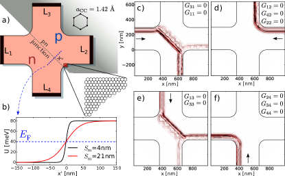
The probability currents obtained for T, meV and electron incident from different leads are shown in Fig. 1(c-f), with snake-like trajectories in Figs. 1(c) and 1(e). Note, that already for this magnetic field value i) the current flows only near the edges Haug1993EdgeState and along the n-p junction and ii) backscattering to the input lead is absent.
The conductance from lead p to denoted as is computed from the Landauer formula
| (3) |
where is the scattering transmission amplitude that electron entering the device at lead p in mode will leave the device at lead in mode n. The summation runs over all propagating modes in the leads and stands for the conductance quantum . For more details about the applied computational method see e.g. Sorensen2009 ; Kolasinski2016 ; Zwierzycki2008 .
The conductance matrix elements DattaBook for the four-terminal device are determined from solution of the scattering problem according to Eq. (3)
with
In the quantum Hall conditions some elements of this matrix are zero (see Figs. 1(c-f)). In our device the quantum Hall edge transport appears for T, and then the conductance matrix acquires the form
Additionally, we have and with being the spin degenerated filling factors in the p/n-regions. In the linear transport conditions the current in each of the leads is given by for a given bias. We choose and to be a source-drain electrodes – with the source , and the drain potentials, respectively. Terminals and are used as voltage probes, which amounts in and so (the plus sign stands for the current that enters the device). The condition immediately implies . This fact can be also deduced from Fig. 1(d) – the current from the drain terminal passes to without scattering. From the form of the second row of the matrix, we have . Hence, in the quantum Hall conditions the current flow is determined uniquely by matrix element, which is studied in detail below.
III Results
III.1 Conductance oscillations due to snake orbits
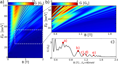
Figure 2(a) shows the conductance as a function of the magnetic field and the Fermi energy. The result contains an oscillatory pattern – marked with the dashed rectangle – similar to the one found Rickhaus2015 experimentally and identified with formation of snake orbits along the n-p junction. The snake states oscillations are visible in a quite large range of both and . For further studies we fix the value of Fermi energy meV and analyze the results as a function of magnetic field. The zoomed fragment of Fig. 2(a) near meV is depicted in Fig. 2(b) and the cross section of the plot for meV is given in Fig. 2(c).
Classically, these oscillations can be understood as due to the variation of the cyclotron orbits [with radius ] as a function of . The electron current can be then sent to either or lead, depending on the value of . Figs. 3(a-e) show the electron current distribution for the electron incident from the lead at meV. The values of the external magnetic field that are denoted by the corresponding letters in Fig. 2(c). Besides the current confinement along the n-p junction one notices deflection of the electron paths, in particular in the p-type (upper right) region of the device, with a radius that decreases with the external magnetic field.
In terms of the quantum transport theory, the snake orbits along the n-p junction – similarly as the skipping orbits Stegmann2015 near the edge of the sample – appear as a result of superposition of Landau level states
| (4) |
where and denote the th Fermi level wave vector and the corresponding transverse mode, respectively. The scattering amplitudes depend on specific boundary conditions.
For simplicity let us assume that the particle is propagating along the direction. For the case when the electron density does not depend on and there is no room for the density variation along the edge or the junction. In this case the idea of the classical cyclotron orbit is irrelevant. For superposition of two or more modes the density results from a superposition of modes with different Fermi wave vectors, leading to the oscillating pattern.
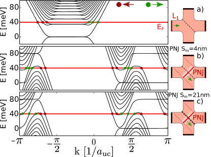
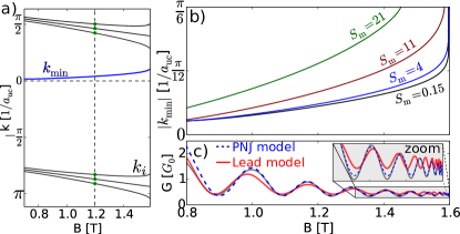
Figure 4(a) shows the dispersion relation for a horizontal channel in lead which is denoted by the green arrow in the inset. For T there are three modes which are propagating to the right (green dots) and three modes for opposite direction (red dots). The wave vectors can be computed from condition Sorensen2009 ; Zwierzycki2008 . In Fig. 4(b) we show dispersion relation for a channel created along the n-p junction of width nm (see the inset). For the junction the number of right-propagating Landau levels is now doubled (six right and six left propagating modes). The doubling of the states in the n-p junction was recently discussed for step-like junctions in Ref. Mele2015SnakeSym with reference to the Bogoliubov quasiparticles and can be explained as a result of coupling the n-type and the p-type conductivity regions – in this case with three conduction and three valence bands at each side of the junction.
We find that the state doubling is not always present in smooth junctions of a finite width – see e.g. Fig. 4(b-c) where a small shift of Fermi energy line will decrease the number of right-moving modes from 6 to 4. The slope of the energy bands as function of the width of the junction changes: the plateaux at the extrema of the bands get narrower in (c.f. the bottoms of the bands in Fig. 4(b) and (c)) for increased , which results in particular in a stronger dependence of the Fermi wave vectors on both and off the band extrema. In Fig. 5(a) we show the evolution of the first six Fermi wave vectors for right-moving modes as a function of magnetic field. The black lines correspond to nm.
The conductance oscillations of Fig. 2(c) can be explained by the superposition of the modes propagating along the junction. We consider the Fermi wave vectors and look for the closest pair of ’s that correspond to the positive velocity . A superposition [see Eq. (4)] of these two modes produces a charge density variation of the largest wavelength ,
| (5) |
Within the range of the magnetic field from T to 1.6 T the minimal distance between the right-going wave vectors appears for the two lowest ones in Fig. 5(a) and the two highest ones. Both distances are found equal. For a superposition of the two modes with the closest wave vectors . Hence the charge density along the junction can be put in a form . The last term is responsible for the oscillations of the density along the junction, and the conductance depends on the destination of the current that reaches the end of the n-p junction at its contact with the edge. At that point the electron current reaches either or . The oscillations of Fig. 2(c) can be described by a a simple phenomenological formula
| (6) |
where the exponential part accounts for the observed decay of the oscillations at high and nm is the length of the junction.
The decrease of the amplitude for higher magnetic field can be understood based on the recent Ref. szaczen , which shows that the transmission coefficient for electron traveling through the n-p junction of a finite width is below 1. Here we consider the junction with nm which according to Ref. szaczen gives the transmission probability . Now, if we increase the magnetic field the number of times that electron passes across the n-p interface increases, hence the reduction of the conductance oscillations amplitude.
The results of the fit with formula (6) for the dispersion relation for the n-p junction [Fig. 4(b)] are denoted as the ”PNJ model” in Fig. 5(c) – the dashed blue line, which above 0.9T agrees perfectly with the numerical conductance. A similar analysis was performed in Ref. Milovanovic2014 but for the dispersion relation of the input lead and not the n-p junction itself. The fit for the dispersion relation of the input lead is given by the red line in Fig. 5(c), in which the agreement is not as good as for the ”PNJ model”. Note, that the fit becomes even worse for a larger magnetic fields, where the out of phase range is visible (see zoomed area in Fig.5(c)). A distinct shift can also be spotted in Fig. 4(f) of Ref. Milovanovic2014 between the model and numerical values, however at lower . The present result indicate that the properties of the band structure of the n-p junction as the conducting channel precisely determine the period of the conductance oscillations on the magnetic field scale in the quantum Hall conditions.
III.2 Imaging the snake states
III.2.1 Weak perturbation
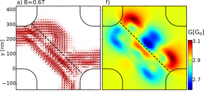
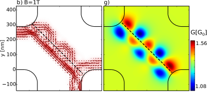
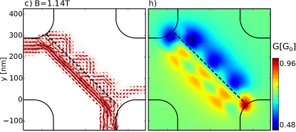
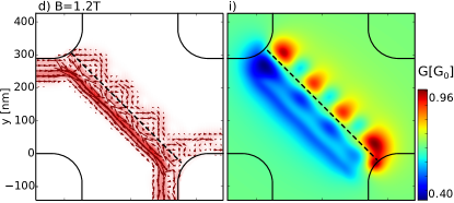
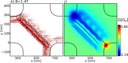
As weak perturbation we consider the tip potential of meV – four times smaller than the Fermi energy. In Figs. 3(f-i) we show the SGM conductance maps for the current distribution given in the left column in Fig. 3(a-e).
The conductance does react to the external perturbation – but only for the scanning probe near the n-p junction. No effect is observed for the tip in the leads. The tip deflects the trajectory to or leads but no backscattering is present which is characteristic to the quantum Hall conditions, hence the flat maps for the probe above the leads.
Figures 3(a,f) correspond to the magnetic field where a conductance peak [Fig. 5(c)] is observed. For this magnetic field the cyclotron radius is comparable to the length of the n-p junction. The SGM image [Fig. 2(f)] does not resolve the details of this orbit. Moreover, here and for other values the SGM maps have an approximate symmetry with respect to the inversion through the bisector of the junction (here line) which is missing in the current plots.
For the subsequent conductance peak marked by "b)" in Fig. 2(c) the cyclotron radius of the deflected electron trajectory [Fig. 5(c)] is already times shorter than [see Fig. 3(b)] and the distance between the extrema of conductance map [Fig. 3(g)] along the junction is comparable to the cyclotron radius. This also found for higher magnetic fields – Fig. 3(c,h), 3(d,i) and 3(e,j), although the visibility of the oscillation becomes unequal at the opposite sides of the junction. The non-transparency of the finite-width junction for electrons szaczen , discussed in the context of Fig. 5(c) is one of the possible reasons responsible for the reduction of the conductance visibility at high magnetic field.
III.2.2 Strong perturbation
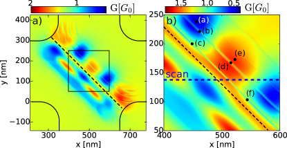
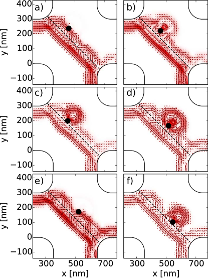
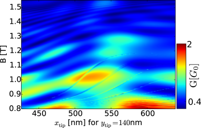
The SGM images for a stronger tip potential meV and T are displayed in Fig. 6 – to be compared with Fig. 3(b) for meV. The asymmetry of the plot between the n and p sides of the junction is increased for larger . Moreover, a number of resonances is found at the p side at lines parallel to the junction. The current density plots for tip location over the points indicated in Fig. 6(b) are displayed in Fig. 7. The resonances are related to current loops that encircle the tip. The current loops are found for the tip on the p side only. The tip potential repels the carriers on the conduction band side of the junction. The currents on the n-side simply avoid the perturbation and no loop of current is found. For the carriers on the valence band side the potential maximum induced by is attractive and thus it supports a quasi-bound state. The exact positions of the resonances depend on the magnetic field in a periodic manner – which is related to the Aharonov-Bohm effect for the current circulation around the tip that couples to the junction current. The conductance across the junction is displayed in Fig. 8 along the dashed line marked in Fig. 6(a) as a function of the external magnetic field. For lower magnetic fields the resonances are found also for the tip near the n-p junction on the n side. For a given tip location the spacing between the subsequent resonances depends on the magnetic field. For higher magnetic fields the clockwise loop that is seen in Fig. 7 is made tighter by the Lorentz force which acts to the right of the current orientation on the p conductivity side. For a reduced radius of the current loop the magnetic field period corresponding to a flux quantum is increased.
III.3 Conductance maps for wider n-p junctions
So far we have discussed the case of a thin junction with nm. From the discussion in Section III.A we know that the width of the junction strongly affects the dispersion relation. We calculated the conductance at meV (as in Fig. 2(c)) as a function of the junction width and the magnetic field. In the result presented in Fig. 9(a) one notices that (i) the resonance lines bend towards lower magnetic field as is increased and (ii) the amplitude of the oscillations decreases with . The feature (i) results from the fact that the spacing between the nearest vectors is increased for wider junctions and at higher magnetic field [Fig. 5(b)]. The corresponding resonances appear for smaller magnetic field values at larger . The finding (ii) seems due to a decreased transparency of the junction with its width found recently in Ref. szaczen . To summarize, we find that for a smooth junction snake orbits appear for lower magnetic fields but at the expense of the visibility of oscillations.
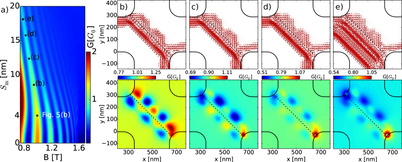
Figures 9(b-e) show the probability current plots and SGM conductance maps for the work points marked in Fig. 9(a) and meV along a selected resonance line. One may see that once we increase the snake features become less resolved both in the current plots and the conductance maps. The current along the n side increases with . The deflected trajectories remain at the p side, where also the amplitude of the conductance map remain stronger than on the n side. In Fig. 9(e) the number of spin degenerated modes is 5 instead of 3, hence the current plot contains additional features from higher modes. However, in the corresponding SGM image no additional features are found.
IV Summary and conclusions
We have discussed the conductance mapping of the snake orbits confined at the n-p junction in graphene. We indicated a precise relation of the conductance oscillations at the magnetic field scale with the Fermi wavelengths of the n-p junction as a waveguide. We found that the maps of conductance contain oscillating patterns along the junction with the period of the oscillation that is close to the period of the snake orbit. The visibility of the map decreases with the external magnetic field due an increased number of the electron passages across the junction and a non-ideal transparency of the n-p junction of a finite width. The conductance maps are found to be nearly symmetrical across the bisector of the junction with an asymmetry between the n- and p- sides. For stronger tip potentials resonant quasi-bound states are formed under the tip at one of the junction sides. The interference of the quasi-bound states with the junction currents produces resonances parallel to the junction with positions that react strongly to the external magnetic field via the Aharonov-Bohm phase shift. We demonstrated that the width of the n-p interface affects the oscillation period and the visibility of the conductance maps.
Acknowledgments
This work was supported by the National Science Centre (NCN) according to decision DEC-2015/17/B/ST3/01161. The calculations were performed on PL-Grid Infrastructure.
References
- (1) A. H. Castro Neto, F. Guinea, N. M. R. Peres, K. S. Novoselov, and A. K. Geim, Rev. Mod. Phys. 81, 109 (2009)
- (2) K. Bolotin, K. Sikes, Z. Jiang, M. Klima, G. Fudenberg, J. Hone, P. Kim, and H. Stormer, Solid State Commun. 146, 351 (2008)
- (3) L. Banszerus, M. Schmitz, S. Engels, M. Goldsche, K. Watanabe, T. Taniguchi, B. Beschoten, and C. Stampfer, Nano Lett. 16, 1387 (2016)
- (4) T. K. Ghosh, A. De Martino, W. Häusler, L. Dell’Anna, and R. Egger, Phys. Rev. B 77, 081404 (2008)
- (5) D. A. Abanin and L. S. Levitov, Science 317, 641 (2007)
- (6) J. Tworzydło, I. Snyman, A. R. Akhmerov, and C. W. J. Beenakker, Phys. Rev. B 76, 035411 (2007)
- (7) V. V. Cheianov, V. Falḱo, and B. L. Altshuler, Science 315, 1252 (2007)
- (8) S. Chen, Z. Han, M. Elahi, K. M. Habib, L. Wang, B. W. Y. Gao, T. Taniguchi, K. Watanabe, J. Hone, A. Ghosh, and C. Dean, Science 353, 6307 (2016)
- (9) P. Rickhaus, R. Maurand, M.-H. Liu, M. Weiss, K. Richter, and C. Schönenberger, Nat. Commun. 4, 2342 (2013)
- (10) T. Taychatanapat, J. Y. Tan, Y. Yeo, K. Watanabe, T. Taniguchi, and B. Özyilmaz, Nat. Commun. 6, 6093 (2015)
- (11) G.-H. Lee, G.-H. Park, and H.-J. Lee, Nat Phys 11, 925 (2015)
- (12) M.-H. Liu, C. Gorini, and K. Richter, arXiv:1608.01730
- (13) J. R. Williams, L. DiCarlo, and C. M. Marcus, Science 317, 638 (2007)
- (14) D. A. Abanin and L. S. Levitov, Science 317, 641 (2007)
- (15) B. Huard, J. A. Sulpizio, N. Stander, K. Todd, B. Yang, and D. Goldhaber-Gordon, Phys. Rev. Lett. 98, 236803 (2007)
- (16) B. Özyilmaz, P. Jarillo-Herrero, D. Efetov, D. A. Abanin, L. S. Levitov, and P. Kim, Phys. Rev. Lett. 99, 166804 (2007)
- (17) J. R. Williams, T. Low, M. S. Lundstrom, and C. M. Marcus, Nat. Nanotechnol. 6, 222 (2011)
- (18) M. Barbier, G. Papp, and F. M. Peeters, Appl. Phys. Lett. 100, 16 (2012)
- (19) N. Davies, A. A. Patel, A. Cortijo, V. Cheianov, F. Guinea, and V. I. Fal’ko, Phys. Rev. B 85, 155433 (2012)
- (20) J. R. Williams and C. M. Marcus, Phys. Rev. Lett. 107, 046602 (2011)
- (21) P. Carmier, C. Lewenkopf, and D. Ullmo, Phys. Rev. B 84, 195428 (2011)
- (22) J.-C. Chen, X. C. Xie, and Q.-F. Sun, Phys. Rev. B 86, 035429 (2012)
- (23) A. Cresti, G. Grosso, and G. P. Parravicini, Phys. Rev. B 77, 233402 (2008)
- (24) S. P. Milovanović, M. Ramezani Masir, and F. M. Peeters, J. Appl. Phys 115, 043719 (2014)
- (25) S. P. Milovanović, M. Ramezani Masir, and F. M. Peeters, Appl. Phys. Lett. 105, 123507 (2014)
- (26) P. Rickhaus, P. Makk, M.-H. Liu, E. Tóvári, M. Weiss, R. Maurand, K. Richter, and C. Schönenberger, Nat. Commun. 6, 6470 (2015)
- (27) Y. Liu, R. P. Tiwari, M. Brada, C. Bruder, F. V. Kusmartsev, and E. J. Mele, Phys. Rev. B 92, 235438 (2015)
- (28) M. Zarenia, J. M. Pereira, F. M. Peeters, and G. A. Farias, Phys. Rev. B 87, 035426 (2013)
- (29) L. Oroszlány, P. Rakyta, A. Kormányos, C. J. Lambert, and J. Cserti, Phys. Rev. B 77, 081403 (2008)
- (30) J. E. Müller, Phys. Rev. Lett. 68, 385 (1992)
- (31) B. Szafran and F. M. Peeters, Europhys. Lett. 70, 810 (2005)
- (32) M. A. Topinka, B. J. LeRoy, S. E. J. Shaw, E. J. Heller, R. M. Westervelt, K. D. Maranowski, and A. C. Gossard, Science 289, 2323 (2000)
- (33) M. A. Topinka, B. J. LeRoy, R. M. Westervelt, S. E. J. Shaw, R. Fleischmann, E. J. Heller, K. D. Maranowski, and A. C. Gossard, Nature 410, 183 (2001)
- (34) A. A. Kozikov, R. Steinacher, C. Rössler, T. Ihn, K. Ensslin, C. Reichl, and W. Wegscheider, Nano Lett. 15, 7994 (2015)
- (35) M. P. Jura, M. A. Topinka, M. Grobis, L. N. Pfeiffer, K. W. West, and D. Goldhaber-Gordon, Phys. Rev. B 80, 041303 (2009)
- (36) H. Sellier, B. Hackens, M. G. Pala, F. Martins, S. Baltazar, X. Wallart, L. Desplanque, V. Bayot, and S. Huant, Semicond. Sci. Technol. 26, 064008 (2011)
- (37) S. Morikawa, Z. Dou, S.-W. Wang, C. G. Smith, K. Watanabe, T. Taniguchi, S. Masubuchi, T. Machida, and M. R. Connolly, Appl. Phys. Lett. 24, 243102 (2015)
- (38) S. Bhandari, G.-H. Lee, A. Klales, K. Watanabe, T. Taniguchi, E. Heller, P. Kim, and R. M. Westervelt, Nano Lett. 16, 1690 (2016)
- (39) V. E. Calado, S.-E. Zhu, S. Goswami, Q. Xu, K. Watanabe, T. Taniguchi, G. C. A. M. Janssen, and L. M. K. Vandersypen, Appl. Phys. Lett. 104 (2014)
- (40) P. Rakyta, A. Kormányos, J. Cserti, and P. Koskinen, Phys. Rev. B 81, 115411 (2010)
- (41) T. Stegmann and A. Lorke, Ann. Phys. (Berlin) 527 (2015)
- (42) T. Taychatanapat, K. Watanabe, T. Taniguchi, and P. Jarillo-Herrero, Nat. Phys. 9, 225 (2013)
- (43) S. Weingart, C. Bock, U. Kunze, F. Speck, T. Seyller, and L. Ley, Appl. Phys. Lett. 95 (2009)
- (44) J. Du, J. Y. Li, N. Kang, L. Lin, H. Peng, Z. Liu, and H. Q. Xu, Nanotechnology 27, 245204 (2016)
- (45) A. S. Mayorov, R. V. Gorbachev, S. V. Morozov, L. Britnell, R. Jalil, L. A. Ponomarenko, P. Blake, K. S. Novoselov, K. Watanabe, T. Taniguchi, and A. K. Geim, Nano Lett. 11, 2396 (2011)
- (46) L. Cohnitz, A. D. Martino, W. Häusler, and R. Egger, arXiv:1608.03469
- (47) M.-H. Liu, P. Rickhaus, P. Makk, E. Tóvári, R. Maurand, F. Tkatschenko, M. Weiss, C. Schönenberger, and K. Richter, Phys. Rev. Lett. 114, 036601 (2015)
- (48) B. Szafran, Phys. Rev. B 84, 075336 (2011)
- (49) H. H. B. Sørensen, P. C. Hansen, D. E. Petersen, S. Skelboe, and K. Stokbro, Phys. Rev. B 79, 205322 (2009)
- (50) K. Kolasiński, B. Szafran, B. Brun, and H. Sellier, Phys. Rev. B 94, 075301 (2016)
- (51) R. J. Haug, Semicond. Sci. Technol. 8, 131 (1993)
- (52) M. Zwierzycki, P. A. Khomyakov, A. A. Starikov, K. Xia, M. Talanana, P. X. Xu, V. M. Karpan, I. Marushchenko, I. Turek, G. E. W. Bauer, G. Brocks, and P. J. Kelly, Phys. Stat. Sol. (b) 245, 623 (2008)
- (53) S. Datta, Electronic Transport in Mesoscopic Systems (Cambridge University Press, Cambridge, 1997)