Development of Yttrium alloy ion source and its application in nanofabrication
Abstract
We present a new YAuSi Liquid Metal Alloy Ion Source (LMAIS), generating focused ion beams of yttrium ions, and its prospective applications for nanofabrication, sample preparation, lithographic and implantation processes. Working parameters of the AuSiY LMAIS are similar to other gold-silicon based LMAIS. We found anomalously high emission current of triple charged Yttrium ions. Influence of Yttrium implantation on optical qualities of the implanted ion-ensembles is shown in luminescence of co-implanted Erbium ions.
I Introduction and motivation
Focused ion beams (FIB) have a lot of applications today, which vary from micro- and nano-machining of different structures Nellen et al. (2006); Sridhar et al. (2012); Lacour et al. (2005); Bischoff et al. (2016) to creation of robust and scalable quantum systems Nadezhda Kukharchyk, Shovon Pal, Jasper Rödiger, Arne Ludwig, Sebastian Probst, Alexey V Ustinov, Pavel Bushev (2014); Probst et al. (2014); Kukharchyk et al. (2016); Siyushev et al. (2014); Kornher et al. (2016); Zhong et al. (2015). In latest quantum information research, ion implantation became an irreplaceable tool in preparation of spin-ensembles in solid state matrix Pezzagna et al. (2010); Meijer et al. (2006); Babinec et al. (2010), which in particular relates to rare-earth (RE) spin-ensembles Nadezhda Kukharchyk, Shovon Pal, Jasper Rödiger, Arne Ludwig, Sebastian Probst, Alexey V Ustinov, Pavel Bushev (2014); Siyushev et al. (2014); Probst et al. (2014); Xia et al. (2015). Stable gold-silicon LMAIS like AuSiEr, AuSiCe or AuSiPr were repeatedly used in some of these experiments.
With an application of FIBs for spin ensembles preparation, concomitant ion-milling methods are more often required Siyushev et al. (2014); Zhong et al. (2015); Babinec et al. (2010). Typically, this micromachining or milling is done by Ga-ion beams. However, the usage of Ga-beam for milling requires after-etching of milled structures in order to prevent an influence from unavoidably implanted Ga ions Zhong et al. (2015).
Standard host-substrates for rare-earth ions are non-Ga-containing. These typically are Y2SiO5, YVO4, YAlO, Y3Al5O12 etc. Ga-incorporation and thus the above mentioned etching step can be avoided if using Yttrium or Silicon ions for milling. The listed above substrates all have Yttrium ions in their crystalline matrix, and therefore milling of such materials with Yttrium ions could be more desirable and even profitable for RE ions properties.
In this letter, we report on a development of AuSiY LMAIS and its prospective properties in micromachining and substrate nanoformation. First, we discuss the fabrication procedure and working parameters of the source. Then, we demonstrate its applications in preparation of ion- and spin-systems.
II Fabrication of the AuSiY LMIS
The AuSiY LMIS was fabricated in the same procedure as described by Melnikov et al Melnikov et al. (2002). The emitter was fabricated of 0.2 mm Tungsten wire in a common hairpin design. The heating wires were covered by ceramic glue in order to prevent creeping up and wetting of the heating wire with the alloy Melnikov et al. (2002). Fabrication of the needle was made according to the technique described by Prewett and Mair Prewett and Mair (1991).
A preliminary mixture of Au (78.4%), Si (11.6%) and Y (10%) (atomic%) was melted in a vacuum furnace. The LMAIS was filled by dipping it into this molten alloy under high vacuum conditions ( Pa). The alloy melting point is approximately 380∘C.
Working parameters of the source were first verified in a test-chamber (called ‘emitter-maker’), and after that the source was tested in an EIKO 100 FIB system under ultra high vacuum (UHV) conditions ( Pa). Expected emission lifetime of the fabricated source is 1000 hours.
III Experimental results
III.1 Emission parameters
.
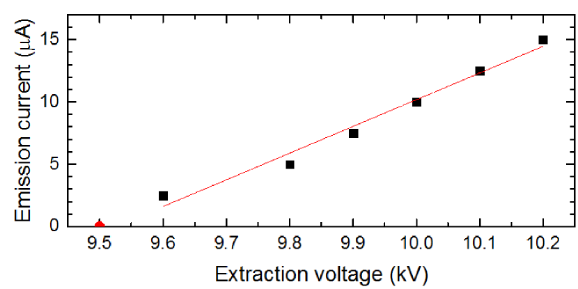
Measured in EIKO 100 FIB, the current-voltage characteristic of AuSiY LMIS is shown in Fig. 1. The emission current was stable during operation times up to 8 hours. The slope of the I-V curve is equal to 43 , which is similar to other Au-based ternary alloys Melnikov et al. (2002); Bischoff et al. (2016).
III.2 Mass-spectrum
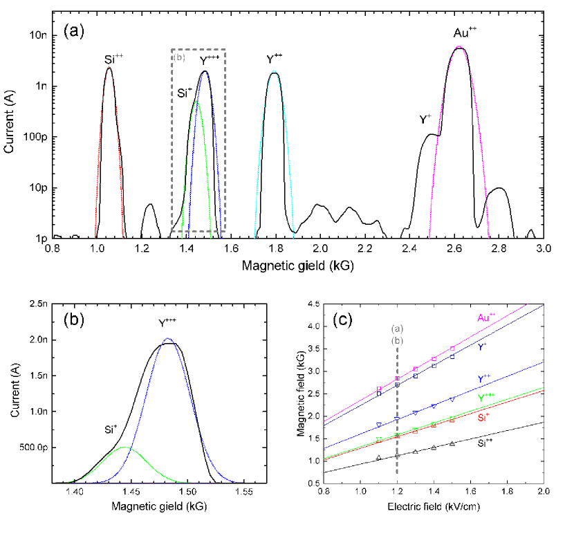
The mass-spectrum of the AuSiY LMIS was measured in the FIB with help of the Wien mass-filter at several electric field values. The resolution of the mass-filter was . Mass-spectrum for magnetic fields from 1 kG to 4 kG at 1.5 kV/cm is shown in Fig. 2 (a). From the superposition of Electric force and Lorentz force, passage of the ions through the filter is given by
| (1) |
where and are respectively the magnetic and electric fields applied by the Wien filter; is the mass of the passing ion and is the atomic mass unit; is the acceleration energy of the ion; is the ion-charge. From (1), we derive the order of ions in the mass-spectrum.
One can see, that the Si+ and Y+++ peaks overlap as their mass-to-charge ratios take very close values: and , see Fig. 2 (b). Thus, the first peak belongs to Si+ and the second one to Y+++. The current of Y+++ ions is approximately three times higher as the current of Si+, which results in a similar number of ions forming the peaks. In Fig. 2 (c), positions of the mass-peaks are given in dependence on the passage condition ((1)).
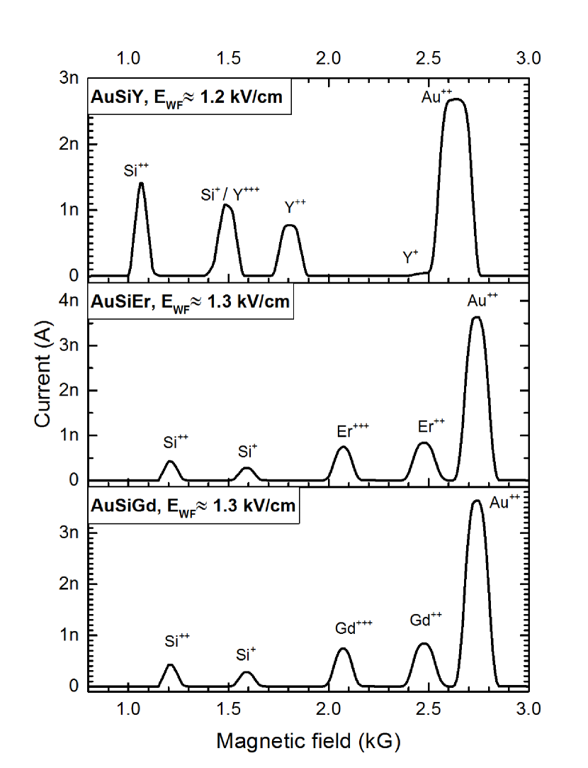
The mass-spectrum of the AuSiY LMIS is similar to mass-spectra of other rare-earth-containing ion sources. To compare, we provide the mass-spectra of AuSiEr and AuSiGd, shown in Fig. 3. The mass-spectra of AuSiEr and AuSiGd were taken at the electric field of 1.3 kV/cm, as noted in the legend. Relative positions of the peaks vary due to different ion masses, however relative intensities of the RE mass-peaks are similar for different sources.
The sputter yield of SiO2 by bombarding with Y++ ions at 10 kV was measured by normal (90∘) incidence of the ion beam onto the surface and it equals 60 atoms/ion.
IV Applications
IV.1 Surface milling
The AuSiY ion-source can be used for milling various photonic structures replacing a Ga-ion-source for the substrates as Y2SiO5 (YSO), YAlO3, YVO4, Y3Al5O12 etc. Y and Si ions can be well-separated in the mass-spectrum and Y++ ion can be selected. For the materials like Y2SiO5, mixed peak Si+/Y++ can be used without separation of the Y and Si ions. This will allow to avoid contamination of the surface layers with gallium ions and the necessity to use etching methods afterwards. Thus, it leads to a more clean fabrication process.
IV.2 Co-doping effect
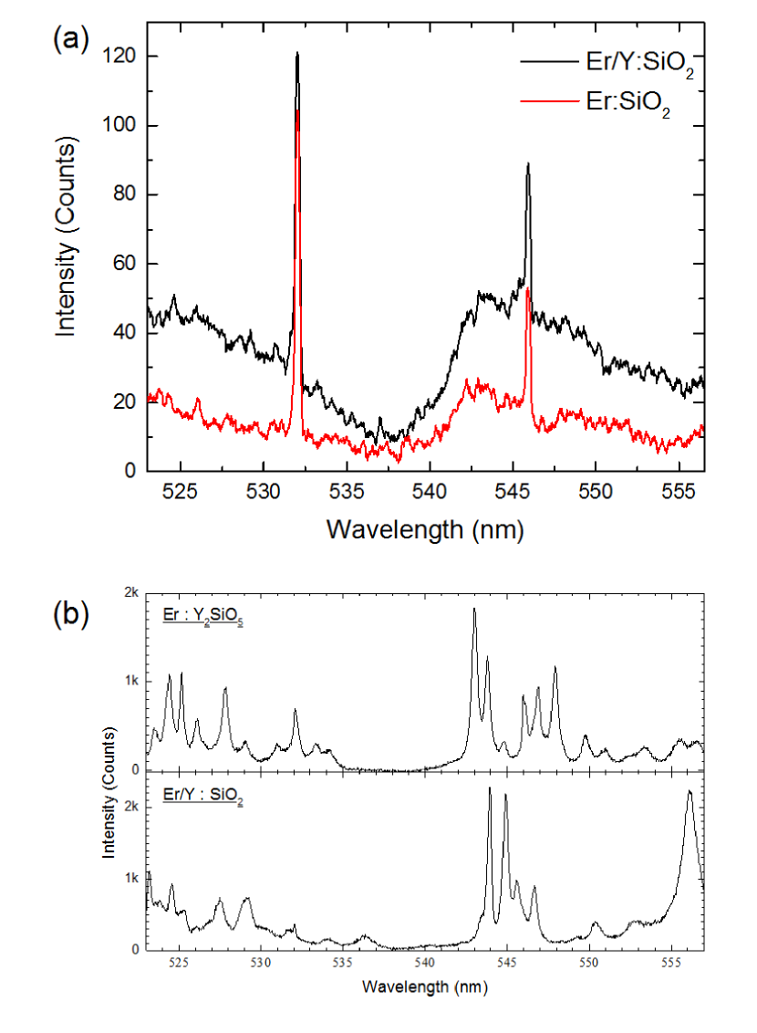
We have implanted SiO2 substrates with Erbium ions, part of which was co-implanted with Yttrium ions. A comparison of the following luminescence is shown in Fig. 4 (a). The samples were excited with 638 nm by an upconversion process in a confocal regime, and 4S3/2/2HI15/2 transitions of Erbium were observed. The Yttrium fluence was equal to cm-2, and the Erbium fluence - to cm-2. It can be seen from the spectra that the intensity of Erbium luminescence is twice enhanced in the presence of Yttrium ions.
IV.3 Nano-crystal formation
In numerical works, chemical methods of forming YSO nanoparticles out of SiO2 and Y2O3 wann2009; Wang et al. (2010); Marinovi et al. (2007); Taghavinia et al. (2004) were demonstrated. We would like to emphasize here the creation of YSO nanoparticles in a porous SiO2 matrix, as described by Taghavinia et al Taghavinia et al. (2004). There, a porous SiO2 matrix is soaked with Yttrium and Europium solutions, dried out and annealed. In the result, Eu-doped YSO nanoparticles are formed in the SiO2 matrix.
We propose, a similar result can be reached with implantation of Yttrium and Europium (Erbium, other rare earth) into the SiO2 substrate. Or similarly, one can use Al2O3 substrates to form Y3Al5O12 (YAG) nanocrystals. These two methods would require a proper Yttrium fluence and annealing procedure.
For a demonstration, we have doped SiO2 substrates with Erbium ( cm-2) and Yttrium ( cm-2) and annealed those in air for several hours. Most of the sample area had broad luminescent peaks, as shown in Fig. 4 (a), which come from variations in crystallographic symmetries of the SiO2-glass (see for comparison luminescence of annealed/non-annealed Er:YSO in Kukharchyk et al. Nadezhda Kukharchyk, Shovon Pal, Jasper Rödiger, Arne Ludwig, Sebastian Probst, Alexey V Ustinov, Pavel Bushev (2014)). However, spots with defined repetitive symmetries were formed; this can be seen from the optical spectrum in Fig. 4 (b). To compare, a spectrum of Erbium implanted Y2SiO5 is shown in Fig. 4 (b) as well. It cannot be concluded here if a different phase of Y2SiO5 or even Y2SiO7 was formed. Nevertheless, it demonstrates that with such a local implantation, nano-particles/-clusters of rare-earth-doped YSO can be created and applied in various modern research.
V Conclusion
We have reported on a fabrication of a stable AuSiY LMAIS. AuSiY LMAIS has a high Yttrium-ion current and high sputter rate. Emitting properties of the source are similar to the other AuSiRE ion-sources. In the mass-spectrum, overlapping Si+/Y+++ peaks are well separated already at 1.5 kV/cm. AuSiY LMAIS can be applied in both micromachining and fabrication of luminescent nanoparticles for quantum optics and quantum information research.
VI Acknowledgement
Authors would like to thank Roman Kolesov, Kangwei Xia and Jörg Wrachtrup for the possibility of optical measurements.
References
- Nellen et al. (2006) P. M. Nellen, V. Callegari, and R. Brönnimann, Microelectronic Engineering 83, 1805 (2006).
- Sridhar et al. (2012) M. Sridhar, D. K. Maurya, J. R. Friend, and L. Y. Yeo, Biomicrofluidics 6, 012819 (2012).
- Lacour et al. (2005) F. Lacour, N. Courjal, M.-P. Bernal, A. Sabac, C. Bainier, and M. Spajer, Optical Materials 27, 1421 (2005).
- Bischoff et al. (2016) L. Bischoff, P. Mazarov, L. Bruchhaus, and J. Gierak, Applied Physics Reviews 3, 021101 (2016).
- Nadezhda Kukharchyk, Shovon Pal, Jasper Rödiger, Arne Ludwig, Sebastian Probst, Alexey V Ustinov, Pavel Bushev (2014) A. D. W. Nadezhda Kukharchyk, Shovon Pal, Jasper Rödiger, Arne Ludwig, Sebastian Probst, Alexey V Ustinov, Pavel Bushev, physica status solidi (RRL) - Rapid Research Letters 8, 880 (2014), arXiv:arXiv:1406.5371 .
- Probst et al. (2014) S. Probst, N. Kukharchyk, H. Rotzinger, A. Tkal??ec, S. W??nsch, A. D. Wieck, M. Siegel, A. V. Ustinov, and P. A. Bushev, Applied Physics Letters 105, 2012 (2014), arXiv:1409.7667 .
- Kukharchyk et al. (2016) N. Kukharchyk, S. Shvarkov, S. Probst, K. Xia, H.-W. Becker, S. Pal, S. Markmann, R. Kolesov, P. Siyushev, J. Wrachtrup, A. Ludwig, A. V. Ustinov, A. D. Wieck, and P. Bushev, Journal of Luminescence , (2016).
- Siyushev et al. (2014) P. Siyushev, K. Xia, R. Reuter, M. Jamali, N. Zhao, N. Yang, C. Duan, N. Kukharchyk, A. D. Wieck, R. Kolesov, and J. Wrachtrup, Nature Communications 5, 3895 (2014).
- Kornher et al. (2016) T. Kornher, K. Xia, R. Kolesov, N. Kukharchyk, R. Reuter, P. Siyushev, R. Stöhr, M. Schreck, H.-W. Becker, B. Villa, A. D. Wieck, and J. Wrachtrup, Applied Physics Letters 108 (2016), http://dx.doi.org/10.1063/1.4941403.
- Zhong et al. (2015) T. Zhong, J. M. Kindem, E. Miyazono, and A. Faraon, Nat Commun 6 (2015).
- Pezzagna et al. (2010) S. Pezzagna, B. Naydenov, F. Jelezko, J. Wrachtrup, and J. Meijer, New Journal of Physics 12, 65017 (2010).
- Meijer et al. (2006) J. Meijer, T. Vogel, B. Burchard, I. W. Rangelow, L. Bischoff, J. Wrachtrup, M. Domhan, F. Jelezko, W. Schnitzler, S. A. Schulz, K. Singer, and F. Schmidt-Kaler, Applied Physics A: Materials Science and Processing 83, 321 (2006), arXiv:0508756 [cond-mat] .
- Babinec et al. (2010) T. M. Babinec, J. T. Choy, K. J. M. Smith, M. Khan, and M. Lončar, Journal of Vacuum Science & Technology B 29, 1 (2010), arXiv:1008.1431 .
- Xia et al. (2015) K. Xia, R. Kolesov, Y. Wang, P. Siyushev, R. Reuter, T. Kornher, N. Kukharchyk, A. D. Wieck, B. Villa, S. Yang, and J. Wrachtrup, Physical Review Letters 115, 1 (2015), arXiv:1505.01673 .
- Melnikov et al. (2002) A. Melnikov, T. Gerya, M. Hillmann, I. Kamphausen, W. Oswald, P. Stauche, R. Wernhardt, and A. D. Wieck, Nuclear Instruments and Methods in Physics Research, Section B: Beam Interactions with Materials and Atoms 195, 422 (2002).
- Prewett and Mair (1991) P. D. Prewett and G. L. R. Mair, Focused ion beams from liquid metal ion sources / P.D. Prewett and G.L.R. Mair (Research Studies Press ; Wiley Taunton, Somerset, England : New York, 1991) pp. xi, 332 p.
- Wang et al. (2010) Y. Wang, F. Cheng, C. Li, Z. Tao, and J. Chen, Journal of Alloys and Compounds 508, 554 (2010).
- Marinovi et al. (2007) M. Marinovi, R. Krsmanovi, D. Drami, and I. Zekovi, 112, 975 (2007).
- Taghavinia et al. (2004) N. Taghavinia, G. Lerondel, H. Makino, and T. Yao, Nanotechnology 15, 1549 (2004).