∎
33institutetext: 2:Institute of Space and Astronautical Science, Japan Aerospace Exploration Agency, Sagamihara, Kanagawa 252-5210, Japan
44institutetext: 3: Graduate School of Science, Nagoya University, Chikusa, Nagoya 464-8602, Japan
55institutetext: 4:Department of Space and Astronautical Science, the Graduate University for Advanced Studies, Sagamihara, Kanagawa 252-5210, Japan
66institutetext: *:corresponding author 66email: wada@ir.isas.jaxa.jp
Fabrication and Analysis of Three-Layer All-Silicon Interference Optical Filter with Sub-Wavelength Structure toward High Performance Terahertz Optics
Abstract
We propose an all-silicon multi-layer interference filter composed solely of silicon with sub-wavelength structure (SWS) in order to realize high performance optical filters operating in the THz frequency region with robustness against cryogenic thermal cycling and mechanical damage. We demonstrate fabrication of a three-layer prototype using well-established common micro-electro-mechanical systems (MEMS) technologies as a first step toward developing practical filters. The measured transmittance of the three-layer filter agrees well with the theoretical transmittances calculated by a simple thin-film calculation with effective refractive indices as well as a rigorous coupled-wave analysis simulation. We experimentally show that SWS layers can work as homogeneous thin-film interference layers with effective refractive indices even if there are multiple SWS layers in a filter.
Keywords:
Terahertz filter Silicon Sub-wavelength structure Micro-electro-mechanical systems technology Rigorous coupled-wave analysis1 Introduction
Optical band-pass filters (OBPFs) are essential components for photometric observations to obtain both color and spatial information simultaneously. High performance OBPFs with rectangular transmission spectrum profiles are critical for precision and dependability. In the THz frequency region, robustness against cryogenic thermal cycling is required to obtain high-sensitivity observations because the OBPFs must be cooled to avoid thermal background noise from the filter itself. Mechanical strength is also required in space applications for components to endure stresses from rocket launching. Furthermore, robustness in filters against rapid decompression and extremely large acoustic vibrations is required for the next-generation warm-launch cryogenic astronomical telescopes, such as SPICA nakagawa12 , as there will be no vacuum chambers to protect OBPFs.
It is, however, still difficult by conventional methods to develop high performance OBPFs for the THz region that have the necessary robustness against cryogenic thermal cycling and mechanical damage. Thin-film multi-layer interference filters are widely used in optical and near infrared wavelength regions Quijada04 . Thin-film filters enable us to realize high performance OBPFs; by increasing the number of layers, nearly rectangular-shaped profiles in the transmission spectra can be obtained Macleod10 . It is favorable for applying the thin-film filters to the THz region, but there is difficultly that only a few materials are known to have good transparency and physical robustness in the region. Furthermore, the conventional thin-film filters are coatings of hetero-materials with different coefficients of thermal expansion (CTE), and thus these heterogeneous multi-layer structures inherently suffer large stresses in cryogenic thermal cycling. Table 1 shows the CTE of PbTe and CdSe, which is commonly used for thin-film filters at the THz region seeley81 . Metal mesh filters are also commonly used as 10 THz-region OBPFs Sako08 , but designing those with transmission spectra with near-rectangular profiles and broad pass-band is difficult in principle, and furthermore freestanding metal thin-films are mechanically fragile.
| PbTe | CdTe | |
|---|---|---|
| CTE | (poly nii64 ) | (a direction iwanaga00 ) |
| () | (crystal houston68 ) | (c direction iwanaga00 ) |
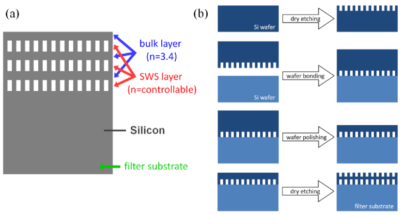
To overcome these difficulties, we proposed an all-silicon (mono-material) multi-layer interference filter with sub-wavelength structure (SWS) Wada10 ; Fig. 1 (a) shows a cross-sectional schematic of the filter. All-silicon filters have superior robustness against cryogenic thermal cycling because it is free from CTE mismatching that plagues conventional heterogeneous thin-film filters. Furthermore, all-silicon filters have high throughput in the THz region owing to low absorption of high-resistivity silicon Edwards85 ; Dai04 . Silicon is also well-suited for mono-material filters because not only it displays good physical and chemical stability but also micro-fabrication processes have been well established for it. We introduce SWS layers to control the refractive indices of each interference layer. According to the effective medium theory (EMT) Brauer94 , a SWS layer behaves as a homogenous medium layer with an effective refractive index. Recently, SWS surfaces were being used widely for optical elements following the fast developments in micro-fabrication technologies Kikuta03 . Multi-layer SWS surfaced devices was also proposed and developed, such as the three-layer birefringent quarter-wave plate consisting of two materials Yu06 .
In this paper, we report on the fabrication of a three-layer all-silicon filter with SWS to demonstrate our proposed fabrication method. We also compare the spectral performance with theoretical calculations to verify that the SWS layers work as homogeneous thin-film interference layers even if there are multiple SWS layers in a filter. The three-layer filter is a first step for future practical multi-layer OBPFs, as in principle multi-layer structures can be fabricated to any degree by iterating the three-layer fabrication cycle.
2 Fabrication
Fig. 1 (b) shows the fabrication procedure of a three-layer all-silicon filter with SWS. We used well-established common micro-electro-mechanical systems (MEMS) technologies: photolithography with dry etching, wafer direct bonding, and wafer chemical mechanical polishing (CMP). We used non-doped high-resistivity () single-crystal silicon (100) wafers fabricated using the floating zone (FZ) method. The diameter and thickness of the wafer was 50 mm and 0.5 mm, respectively. Both sides of the wafer were polished to a mirror surface by CMP. Our AFM observations of the surface after the CMP showed roughness of 0.4 nm RMS. At first, we performed photolithography and dry etching to fabricate a SWS layer on the surface of the wafer. We used deep inductively coupled plasma reactive ion etching (ICP-RIE) Marty05 equipment (Sumitomo Precision Products MUC-21) with SF6 as etching gas and CF4 as passivation, and fabricated deep holes by the Bosch process Laermer96 . Next, we applied wafer direct bonding to create a second layer. The wafer with SWS and a bulk wafer were bonded by a surface activated wafer bonding (SAB) technique Takagi96 using a room-temperature wafer bonding machine (Mitsubishi Heavy Industries MWB-04R). Then, we thinned the wafer to control the thickness of the bulk layer using a grinder (Musashino-denshi MA-200) and diamond particles as abrasives. The wafer was finally polished by CMP to obtain a mirror surface for future SAB process. We further performed photolithography and ICP-RIE processing to fabricate an additional SWS layer. Thus, a three-layer all-silicon filter with SWS was produced.
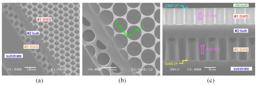
Fig. 2 shows scanning-electron microscope (SEM, Japan Electron Optics Laboratory JSM-5510) images of the fabricated three-layer all-silicon filter with SWS. We measured SWS dimensions and thicknesses of each layer from the SEM images. For convenience, each layer is designated a symbol #(layer number):(medium structure); that is, the SWS layer on the vacuum side is #1:SWS, the bulk layer is #2:bulk, and the SWS layer on the substrate side is #3:SWS. The hole diameters of layers #1:SWS and #3:SWS are 4.9 m and 4.3 m, respectively. The distances between centers of two adjacent holes in layers #1:SWS and #3:SWS are 5.2 m. Thus, the layer porosities of #1:SWS and #3:SWS are 80% and 62%, respectively. The layer thicknesses of #1:SWS, #2:bulk, and #3:SWS are 6.8 m, 6.0 m, and 9.8 m, respectively. We note that the interface between layers #1:SWS and #2:bulk has a round shape resulting from the ICP-RIE process, so that we define the thickness of the #1:SWS layer as a mean depth in the #1:SWS cylindrical holes. The thickness of the #3:SWS layer is defined similarly. We also note that both holes of layers #1:SWS and #3:SWS can be simultaneously observed even in the top view image, Fig. 2 (b), because the three-layer filter was cleaved at a slant.
3 Theoretical calculation
3.1 Methods
We calculated a theoretical transmittance of the fabricated filter (three interference layers on one side of the filter substrate) by following procedure. First, we calculated transmittances and reflectances of only the three interference layers using two calculation methods: a three-layer full simulation using rigorous coupled-wave analysis (RCWA) Moharam86 and a simple three-layer thin-film calculation with effective refractive indices, in order to verify theoretically that SWS layers can work as homogeneous thin-film layers even in filters with multiple SWS layers. Finally, by considering multiple reflections in the filter substrate, we calculated transmittances of the entire filter.
In the three-layer full RCWA simulation, we made a calculation model using the measured SWS dimensions and thicknesses obtained from the SEM images. We also took into account the distance between the central axes of the #1:SWS holes and the #3:SWS holes. In the simulation, the incident angle was and the order of the Fourier coefficients was between -10th and +10th for both x and y directions, marked in Fig. 2 (b). We calculated unpolarized transmittances by averaging the two orthogonal linear polarizations. The RCWA simulation was performed by commercial software (RSoft Design Group DiffractMOD).
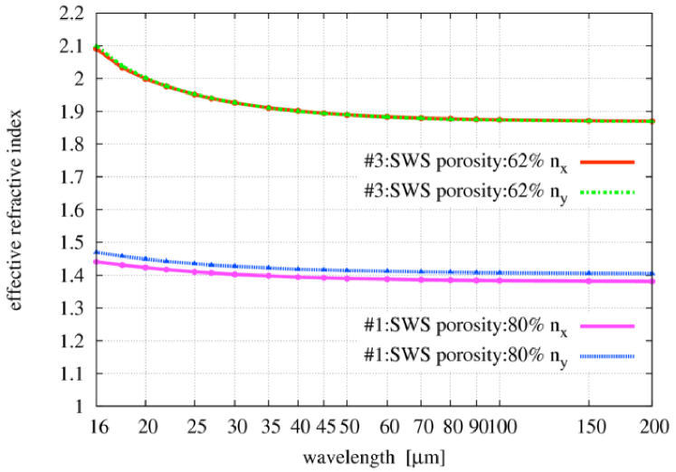
For the simple three-layer thin-film calculation, we estimated the effective refractive indices of layers #1:SWS and #3:SWS by the following procedure. First, we calculated a reflectance for a given light wavelength of one SWS-layer filter (only one SWS-layer on a substrate) as a function of the SWS-layer thickness. This calculation itself was performed using the RCWA simulation. Then, we found the thicknesses where the reflectance takes local minimums. These thicknesses must be odd times of the quarter-wave optical thickness because of interference conditions, because we assumed that the SWS layer was a homogenous dielectric layer. Thus, we determined the effective refractive index from formula, , where was the light wavelength in vacuum and was the smallest thickness that gives the local reflectance minimum. Fig. 3 shows the effective refractive indices of layers #1:SWS and #3:SWS for each orthogonal linear polarization as a function of wavelength. The effective refractive indices exhibit wavelength dispersion, signifying that zeroth-order EMT Brauer94 is no longer valid at shorter wavelength regions. Diffraction, however, does not occurred in the wavelength regions (). Hence, with these effective refractive indices, we can calculate transmittances of the three interference layers for each orthogonal linear polarization, and then by averaging the two, we can calculate the unpolarized transmittances.
In the above calculations, the refractive index of silicon was set to 3.42 (no wavelength dispersion). In the three-layer calculation, we did not consider absorption in silicon because the three interference layers were sufficiently thin that absorption is negligible. In the substrate calculation, however, we considered the extinction coefficients of silicon Edwards85 ; Dai04 because the substrate was thick enough that absorption could not be ignored. We note that the measured transmission spectrum of the bulk silicon wafer agreed well with the calculation using the above-mentioned optical constants.
3.2 Results
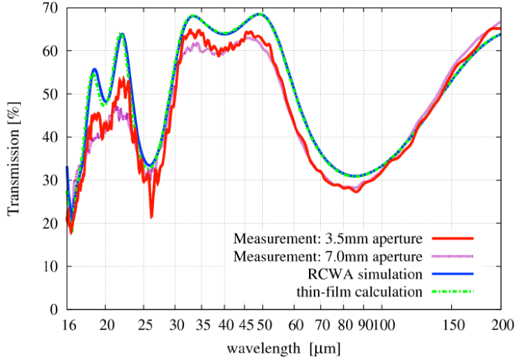
Fig. 4 shows theoretical transmission spectra of the three-layer filter calculated by a three-layer full RCWA simulation and by a simple three-layer thin-film calculation with the effective refractive indices shown in Fig. 3. The calculated transmittance from the full RCWA simulation agrees well with that from the simple thin-film calculation. Therefore, theoretically, the SWS layers can function as homogeneous thin-film layers even if there are multiple SWS layers in a filter.
We remark that we calculated various transmittances using the three-layer full RCWA simulation by changing the distance between the central axes of the #1:SWS and #3:SWS holes, and that the results overlap in the vertical axis resolution in Fig. 4. Thus, we do not need to align the centers of each SWS-layer hole during wafer bonding, enabling us to produce multi-layer all-silicon filters by current MEMS technologies.
4 Experimental results
We measured the transmittance of the three-layer filter by a Fourier transform infrared (FT-IR) spectrometer (BOMEM DA8) at room temperature and under vacuum conditions ( 0.3 Torr). A mercury lamp, a Mylar film, and a deuterated triglycine sulfate (DTGS) pyroelectric detector were used as light source, beam-splitter for the Michelson interferometer, and light detector, respectively. The aperture sizes of the light beam were 3.5 mm and 7.0 mm; the beam incident angle was . The measured transmission spectra are presented in Fig. 4. The spectral resolution was 4.0 cm-1 and the transmittance accuracy was about 10% as evaluated from the scattering of the measured values taken on different days. The fluctuation of the measured transmittance around is due to the degradation in measurement accuracy resulting from poor signal-to-noise ratio. We performed multiple thermal cycling down to LN2 temperature and confirmed that the transmission spectra did not change in our measurement accruracy.
As seen in Fig. 4, measured and theoretical transmittances agree well. In particular, the measured wavelengths where transmittances take local maximum or minimum values correspond well to theoretical values. This is the experimental confirmation of the functioning of the SWS layers as homogeneous thin-film interference layers. Thus, we can save time when designing practical extended multi-layer all-silicon filters because we can estimate the transmission spectra using only the simple thin-film calculation instead of the time-consuming multi-layer full RCWA simulation.
5 Discussion
All-silicon filters can achieve far superior throughput in transmission pass-band because the absorption of silicon in the THz region is sufficiently small. In the fabricated three-layer filter, however, the theoretical maximum transmittance is 70% because of Fresnel reflection at the backside interface between substrate and vacuum. The loss of transmittance by Fresnel reflection vanishes when we fabricate interference layers on both sides of the filter substrate; the maximum transmittance reaches 100% with the precise design of the interference layers.
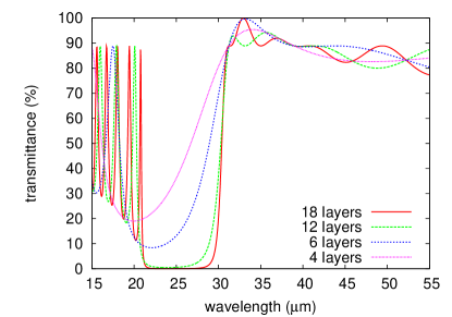
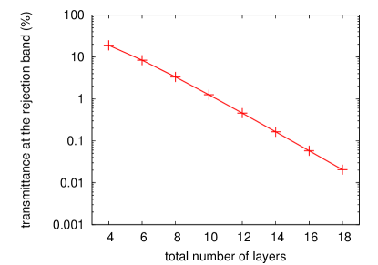
The rejection-band transmittance of the three-layer filter is about 30%, which is not sufficient for practical use (typically below 0.1%). In order to estimate the number of layers which is necessary for practical use, we have designed long wave pass filters (LWPFs) which are commonly used to configure a band-pass filter together with a short wave pass filter (SWPF) at the other side of the substrate. We have designed the LWPFs with quarter wave optical thickness (QWOT) structure of , where S and V represent Si substrate () and the vacuum, and and are the QWOT of Si bulk () and SWS () layers, respectively. The total number of layer is . In a sixteen-layer filter (m=7), the transmittance of the rejection-band falls below 0.1% and the transmission spectrum becomes more rectangular in shape as the number of layers increases (Fig. 5).
The flatness of each interference layer is the key in achieving high performance OBPFs. Different thicknesses of an interference layer within a filter result in different transmission spectra at various positions over the filter. Therefore, especially steep shapes in a transmission spectrum are broken because an observed transmission spectrum from an aperture is an integration of transmission spectra at various filter positions within the aperture. From a filter designing perspective, each layer thickness should be flat to within for an OBPF around the wavelength region. This requirement decreases at longer wavelength to for the wavelength region.
In our fabricated three-layer filter, the layer thicknesses of #1:SWS and #3:SWS are uniform at various filter positions within the measurement accuracy (). The layer thickness of #2:bulk is, however, not uniform; at the transmission-measured position the thickness is , but the thicknesses at +5 mm, -5 mm, and -10 mm away from the transmission-measured position are , , and , respectively. Clearly, the #2:bulk layer has a large gradient in thickness, which is not adequate in practical applications. Indeed, the measured transmittance from the 7.0 mm aperture beam is clearly lower than that from the 3.5 mm aperture beam for wavelengths around and where the transmission spectrum rise steeply (see Fig. 4). The gradient of the #2:bulk layer thickness is also considered as a reason for disagreement between the measured and calculated transmittances around and . This gradient may come from a m-scale particle between the filter and the holder of the grinder during CMP. To produce a flat bulk silicon layer for practical applications, we are planning to use a device layer of a silicon-on-insulator (SOI) wafer.
6 Conclusion
We have fabricated a three-layer all-silicon interference filter with SWS by combining well-established common MEMS technologies. The measured transmission spectrum of the three-layer filter agreed well with theoretical calculations using not only a three-layer full RCWA simulation but also a simple three-layer thin-film calculation with effective refractive indices determined by a one-layer RCWA simulation. We conclude that the SWS layers function as homogeneous thin-film interference layers even if there are multiple SWS layers in a filter, and that we can design transmission spectra of practical extended multi-layer all-silicon filters with SWS using a simple thin-film calculation with effective refractive indices.
Acknowledgements.
The authors are deeply grateful to Mr. Jun Utsumi and Mr. Masahiro Kato at Mitsubishi Heavy Industries, Ltd. for supporting the room-temperature wafer bonding process. This study was supported by the FY2009 and FY2012 Japan Aerospace Exploration Agency President Fund, and FY2010 ISAS/JAXA Basic R&D on onboard equipment.References
- (1) T. Nakagawa, H. Matsuhara, and Y. Kawakatsu, Proc. SPIE 8442, 84420O (2012).
- (2) M. A. Quijada, C. T. Marx, R. G. Arendt, and S. H. Moseley, Proc. SPIE 5487, 244 (2004).
- (3) H. A. Macleod, Thin-Film Optical Filters, 4th ed. (CRC Press, New York, 2010), Chap. 7-8.
- (4) R. Nii, J. Phys. Soc. Jpn. 19, 58 (1964)
- (5) B. Houston, R. E. Strakna, and H. S. Belson, J. Appl. Phys. 39, 3913 (1968)
- (6) H. Iwanaga, A. Kunishige, and S. Takeuchi, J. Mater. Sci. 35, 2451 (2000)
- (7) J. S. Seeley, R. Hunneman, and A. Whatley, Appl. Opt. 20, 31 (1981)
- (8) S. Sako, T. Miyata, T. Nakamura, T. Onaka, Y. Ikeda, and H. Kataza, Proc. SPIE 7018, 701853 (2008).
- (9) T. Wada, H. Makitsubo, and M. Mita, Appl. Phys. Express 3, 102503 (2010).
- (10) D. F. Edwards, in Handbook of Optical Constants of Solids, ed. by E. D. Palik (Academic Press, New York, 1985), p. 568.
- (11) J. Dai, J. Zhang, W. Zhang, and D. Grischkowsky, J. Opt. Soc. Am. B 21, 1379 (2004).
- (12) R. Brauer and O. Bryngdahl, Appl. Opt. 33, 7875 (1994).
- (13) H. Kikuta, H. Toyota, and W. Yu, Opt. Rev. 10, 63 (2003).
- (14) W. Yu, A. Mizutani, H. Kikuta, and T. Konishi, Appl. Opt. 45, 2601 (2006).
- (15) F. Marty, L. Rousseau, B. Saadany, B. Mercier, O. Francais, Y. Mita, and T. Bourouina, Microelectron. J. 36, 673 (2005)
- (16) F. Laermer and A. Schilp, U.S. Patent 5501893 (1996)
- (17) H. Takagi, K. Kikuchi, R. Maeda, T. R. Chung, and T. Suga, Appl. Phys. Lett. 68, 2222 (1996)
- (18) M. G. Moharam and T. K. Gaylord, J. Opt. Soc. Am. A 3, 1780 (1986)