Amplified-reflection plasmon instabilities in grating-gate plasmonic crystals
Abstract
We identify a possible mechanism of the plasmon instabilities in periodically gated two-dimensional electron systems with a modulated electron density (plasmonic crystals) under direct current. The instability occurs due to the amplified reflection of the small density perturbations from the gated/ungated boundaries under the proper phase matching conditions between the crystal unit cells. Based on the transfer-matrix formalism, we derive the generic dispersion equation for the travelling plasmons in these structures. Its solution in the hydrodynamic limit shows that the threshold drift velocity for the instability can be tuned below the plasmon phase and carrier saturation velocities, and the plasmon increment can exceed the collisional damping rate typical to III-V semiconductors at 77 K and graphene at room temperature.
I Introduction
The emission of terahertz radiation from two-dimensional electron systems (2DES) under direct current flow has been observed in a large number of experiments, starting from the pioneering work of Tsui, Gornik and Logan Tsui et al. (1980). At the current stage of technology, the emission from these structures sustains up to the room temperature Dyakonova et al. (2006), its frequency is voltage-tunable from to 2 THz El Fatimy et al. (2010), while the linewidth can be as narrow as GHz Otsuji et al. (2013). It is commonly accepted that the radiation appears as a result of plasmon excitation Tsui et al. (1980); Matov et al. (1997); Mikhailov (1998); Dyakonov and Shur (1993) in 2DES and the subsequent coupling of plasmon to the free-space radiation upon interaction with single Dyakonov and Shur (1993) or multiple Krasheninnikov and Chaplik (1985) metal gates. The periodically gated 2DES typically demonstrate emission of higher power and narrower linewidth Otsuji et al. (2007, 2008, 2013) compared to the plasmonic transistors with a single gate. Despite these experimental advances, there exists no accepted theory on the mechanism of plasmon self-excitation in grating-gated plasmonic nanostructures.
Early works have suggested the excitation of plasmons by hot electrons Chaplik (1985). However, in the latest experiments Otsuji et al. (2013) the emission sets on in a threshold-like manner, which signifies the occurrence of plasma instability. In the simplest case of dc electron flow in 2DES parallel to the conducting gate, the dissipative instabilities Krasheninnikov and Chaplik (1980) can develop at drift velocity equal to the plasmon velocity. A similar estimate of threshold velocity was obtained for amplified transmission of radiation through periodically-gated 2DES with uniform density Matov et al. (1997); Mikhailov (1998). Such high velocity can be hardly achieved in experiment, particularly, due to the choking of electron flow Dyakonov and Shur (1995).
The onset of terahertz emission in grating-gated 2DES at low longitudinal electric field ( kV/cm in Otsuji et al. (2008)) motivated the search of low-threshold plasmon instabilities. In Refs. Ryzhii et al. (2005, 2008); Koseki et al. (2016) it was supposed the latter can emerge due to the transit time effects in the high-field domains of 2DES. However, the transit time effects generally require the deviations from linear relation between current and electric field, e.g. due to velocity saturation. The voltage drop across each cell of experimentally relevant grating-gated 2DES Otsuji et al. (2007) is less than 20 mV, and the transit time effects can be suppressed at such low voltages.

A new class of plasma instabilities based on amplified plasmon reflection in bounded 2DES was put forward by Dyakonov and Shur Dyakonov and Shur (1993). Their threshold velocity is limited only by the carrier scattering by impurities or phonons, and can be made very low in sufficiently clean systems. At the same time, the Dyakonov-Shur (DS) instability relies on essentially asymmetric boundary conditions at the 2DES contacts: the impedance at the drain should be greater than at the source Cheremisin and Samsonidze (1999). Such asymmetry is not present in a weakly biased isolated gated cell in an infinite 2DES (Fig. 1B).
In the present paper, we theoretically show that the reflection-type plasma instabilities can develop in periodically gated 2DES (plasmonic crystals) with a modulated electron density. We find that the travelling waves with quasi-momentum not at the edge of the plasmonic Brillouin zone are generally more unstable than purely periodic waves considered in Ref. Mikhailov (1998). We show that the drift velocity required for the emergence of unstable modes can be well below the plasmon phase velocity. This contrasts to the case of ’plasmonic boom’ instabilities in all-gated plasmonic crystals with a varying carrier density Kachorovskii and Shur (2012) or of a varying width Aizin et al. (2016) that occur at ’superplasmonic’ drift velocities. Remarkably, the proposed mechanism of instability requires neither transit-time nor velocity saturation effects Ryzhii et al. (2005, 2008). It can be thus responsible for the plasmon instabilities and THz emission in grating-gate structures with graphene and GaN channels, where the critical field and saturation velocity are very large Meric et al. (2008).
Our mechanism of instability can be understood as follows. In a single gated cell of plasmonic crystal, the downstream plasmon undergoes an amplified Dyakonov-Shur reflection from the gated/ungated boundary Dyakonov (2008); Sydoruk et al. (2012a). In an isolated gated cell, the reflected upstream wave would be attenuated upon reflection from the opposite boundary. But under the proper phase matching conditions in multigate structures, the fraction of the plasmon energy from the previous cell can compensate the reflection loss of the upstream wave (Fig. 1C). This periodic amplified reflection results in the net instability.
In Sec. II, we derive the generic dispersion equation for the plasmons in a periodically gated 2DES in the presence of the electron drift and discuss the stability of the solutions. In Sec. III, we find the eigenfrequencies and instability increments of the plasmonic modes in the hydrodynamic limit. Section IV discusses the possible experimental manifestations of this instability and further extensions of the model.
II Plasmon dispersion and conditions of instability
To provide a quantitative picture of the instability, we derive the dispersion equation for the travelling waves with a non-zero Bloch phase , where is the quasi-momentum and is the length of plasmonic crystal cell. According to the microscopic studies of wave reflection at the gated/ungated boundarySydoruk et al. (2015a), the net amplitude of wave can be approximated as a sum of the ’fast’ downstream and ’slow’ upstream plasmons both in the gated and ungated sections. This so-called quasi-optical approximation provides sufficient accuracy for long ungated sections and/or high frequencies Karabiyik et al. (2014). We denote the plasmon wave vectors as , where the plus sign stands for the downstream waves, and minus sign – for the upstream waves, the superscripts ’g’ and ’u’ denote the gated and ungated sections, respectively. The amplitudes of electric potential in these waves are denoted as .
Let us compose the vectors . In the neighboring cells of the crystal, they can differ only by the factor . On the other hand, they are related via the transfer matrix of the unit cell , . This leads us to the general dispersion equation Pendry (1994)
| (1) |
where is the identity matrix. The transfer matrix of the unit cell is represented as the product of transfer matrix characterizing the ungated section , the matrix of the wave reflection and transmission at the ungated/gated boundary , the transfer matrix of the gated part , and, finally, the -matrix of another boundary:
| (2) |
The transfer matrices of free wave propagation have the diagonal form
| (3) |
where and are the lengths of the gated and ungated regions, respectively. Keeping in mind the flow-induced non-reciprocity, we can present the -matrix describing the boundary as Sydoruk et al. (2015b)
| (4) |
where and are the reflection and transmission coefficients of the waves incident from the ungated (gated) region. These reflection and transmission coefficients are essentially different due to the presence of electron flow.
Known all elements of -matrices, one readily obtains the dispersion equation for plasmons in drifting 2DEG with grating gate:
| (5) |
where
| (6) |
is the ’modulation depth’ factor. Equation (5) is generic and its functional form does not depend on the transport properties in gated and ungated sections and at the boundaries. In the absence of a drift, it is similar to the plasmon dispersion in a fully gated 2DES with a modulated densityKachorovskii and Shur (2012), or to the photon dispersion in one-dimensional photonic crystals Bendickson et al. (1996) and electron dispersion in the Kronig-Penney potential. All the information about ’bulk’ carrier transport in Eq. (5) is contained in the plasmon wave vectors and , while all the information about boundary transport is enclosed in the coefficients and .
The instability conditions for the waves with the dispersion relation given by (5) can be derived in a very general form. As the system approaches the instability threshold with an increasing drift velocity, the stable anticrossing of the plasmon bands transforms into an unstable one (Fig. 2) Landau et al. (1993). Upon increasing the flow velocity, the plasmon band gap gradually decreases, and the shrinkage of the gap indicates the onset of instability. For a real-valued coefficient , this shrinkage occurs when the absolute value of the right-hand side of Eq. (5) equals unity, while its frequency derivative equals zero. If the frequency dependence of the modulation depth is weak (this assumption will be justified in the next section), the instability conditions can be expressed in a concise form
| (7) | |||
| (8) |
Equations (7) and (8) allow one to determine simultaneously the critical flow velocity, the frequency and quasi-wave vector at which the instabilities occur.
III Analysis of the dispersion relation
The usefulness of Eq. (5) stems from the fact that it can be applied to a wide class of two-dimensional systems, once their plasmon dispersion relations in the presence of drift are known. The calculation of the reflection and transmission coefficients governing the value of can be also done by various methods differing in complexity and accuracy Sydoruk et al. (2012b, 2015a).
For the numerical estimates of the critical velocity and the magnitude of wave increment, we derive the frequency dependencies of the wave vectors within the hydrodynamic model. The latter is justified when carrier-carrier collision frequency exceeds the plasma frequency and the frequency of the carrier collisions with impurities and phonons. Both the theoretical estimates Dyakonov and Shur (1993); Svintsov et al. (2012) and experiments de Jong and Molenkamp (1995); Rudin et al. (2014) support the applicability of the hydrodynamic model up to the terahertz frequencies in III-V 2DEGs and graphene Bandurin et al. (2016). The simultaneous solution of Poisson, Euler and continuity equations leads us to
| (9) | |||
| (10) |
where is the plasma wave frequency, are the carrier drift velocities, is the plasma wave velocity in the absence of drift, , is the carrier density in the ungated region, is the gate-to-channel bias, is the electron effective mass, which we take to be , is the gate dielectric constant.
The determination of the reflection and transmission coefficients requires an imposition of the boundary conditions for the electric potential, drift velocity and carrier density at the gated/ungated interface. If the electron transport obeys the hydrodynamic equations at the transient regions as well, the boundary conditions for the determination of and would represent the continuity of (1) current and (2) carrier energy Kachorovskii and Shur (2012); Aizin et al. (2016). The latter may obtained by integrating the Euler equation across the transient region. However, the length of the transient regions is comparable to the screening length in the 2DEG and is generally smaller than the collision-limited free path. This makes the ballistic description of the transport at the boundary favorable to the hydrodynamic approach.
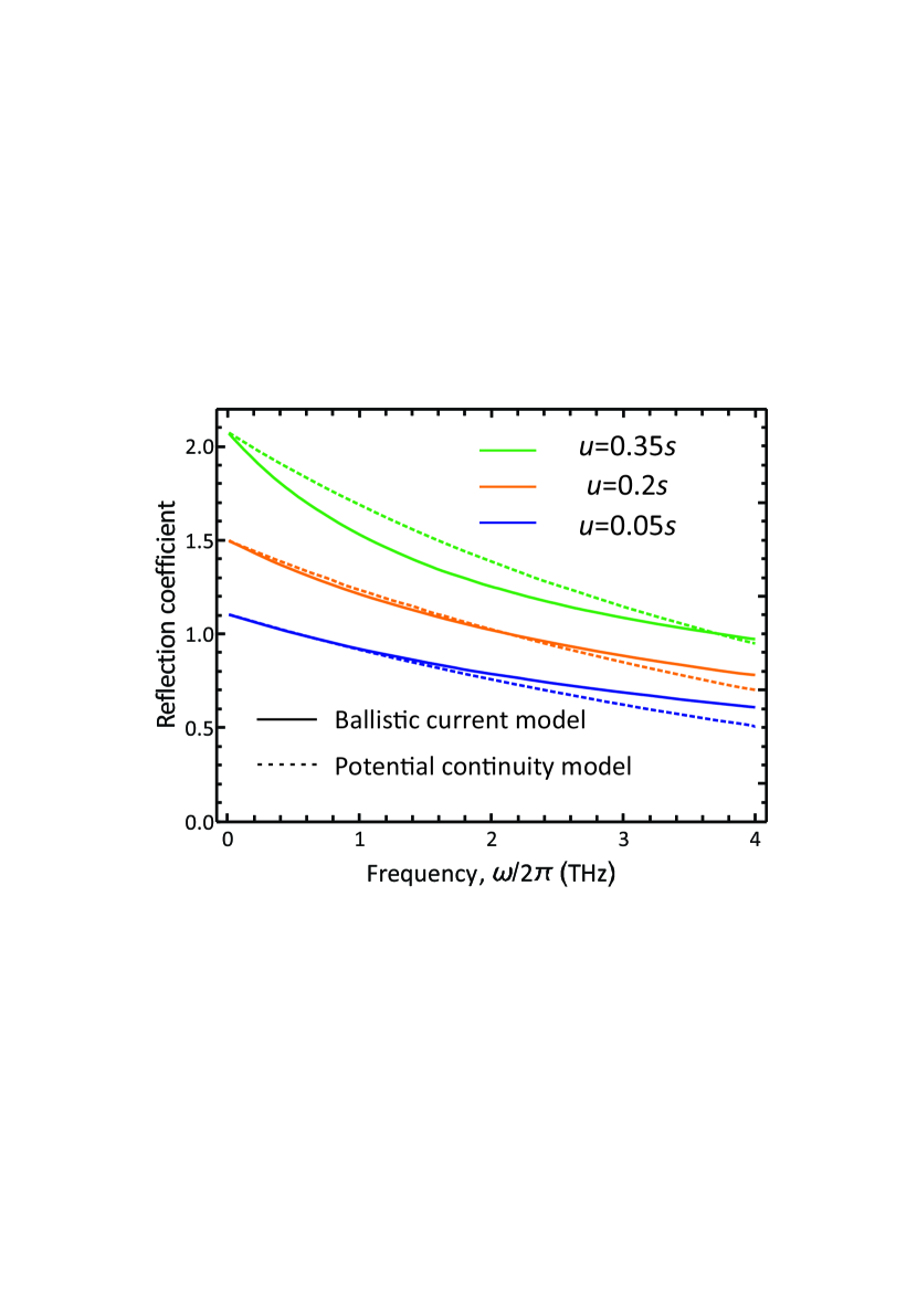
Within the ballistic approach, the current across the boundary is calculated as the difference of particle fluxes supplied by the gated and ungated sections. As a result, the variation of current becomes a linear function of the quasi-Fermi level drop across the boundary, Horio and Yanai (1990), which should be used as the second boundary condition. The explicit form of this relation is presented in Appendix, Eq. 25. However, the reflection coefficient can be determined with a sufficient accuracy (see Fig. 6) if we simply require the continuity of electric potential across the gated/ungated boundary, . This results in the following expressions for the reflection and transmission coefficients:
| (11) | ||||
| (12) |

With the above reflection and transmission coefficients, the dependence has a smooth minimum with the minimal value below unity at any non-zero flow velocity, which justifies the neglect of in the derivation of the instability condition. As seen from Eqs. (7), (6) and (11), the threshold velocity for the instability corresponds to the reflectionless passage of the upstream plasmon from the ungated to the gated sections (). At given frequency , this velocity is
| (13) |
where is the plasmon wavelength in the gated section. In typical experiments Knap et al. (2004), the plasmon wavelength is on the order of hundreds of nanometers, while the gate-to-channel separation is several tens of nanometers. Despite tha fact that the ratio is usually small, a large prefactor of in Eq. (13) provides an extra order of magnitude to this ratio, and the second term in (13) can even exceed unity.
Fig. 2 showing the dispersion curves and plasma instability increments in -based 2DEG under grating gate at different drift velocities substantiates these findings. The lengths of the gated and ungated sections are and , respectively, the gate-to-channel separation is , gate dielectric permittivity , the carrier densities are and . The onset of the instability represents a transformation of a stable-type plasmon band anticrossing to the unstable one via passing through the gapless plasmon bands. In the unstable case, the neighboring branches of the dispersion curves merge through the complex plane corresponding to two complex conjugate solutions of the dispersion equation and for each Bloch phase. For the parameters of Fig. 2, the unstable mode at 2.9 THz appears at which is in precise agreement with formula (13).
Above the threshold velocity, the waves are unstable for a finite range of the quasi-wave vectors (Bloch phases). Generally, these unstable wave vectors lie away from the edges of the Brillouin zone, i.e. their Bloch phase . The reason is that the extrema of the plasmonic bands (being at the edges of Brillouin zone at zero drift velocity) are shifted away by the Doppler effect. Within the unstable domains, the real part of plasmon frequency almost does not depend on the quasi wave vector, while the increment varies abruptly. Expanding the dispersion equation (5) near the band anticrossing at and , we find
| (14) |
where . Equation (14) describes the square-root growth of increment above the critical Bloch phase observed in Fig. 2.

As the drift velocity increases, the branches of plasmon dispersion become denser (Fig. 3). This is explained by the fact that the backward wavevector in the gated region grows as , and at large velocities even a slight variation of the frequency results in strong variations of the right-hand side of dispersion equation (5). One can also observe that the highest increments are achieved at the frequency, for which the modulation depth has the minimal value. This is seen from an arc-shaped envelope of increment curves in Fig. 3: the frequency of THz corresponds to the minimum of and to the maximum of the increment. The deviation of frequency from this value leads to an increase in and decrease in the increment.

It is remarkable that the maximization conditions for the instability increment can be derived analytically. The maximum instability increment is achieved in the middle of the unstable domain with respect to the quasi momentum , and the wider the instability domain is, the larger is the increment. The center of the unstable domain corresponds to zero -derivatives of both left- and right-hand sides (lhs. and rhs.) of Eq. (5). Moreover, the instability increment can be maximized with respect to all other parameters of the problem (gate length, carrier density, etc.) by requiring the maximum difference of lhs. and rhs. of Eq. (5) at the middle of the unstable domain. In this case, the disbalance between the rhs. and lhs. as functions of real frequencies can be compensated only via introduction of a sufficiently large imaginary part of frequency.
The superposition of these requirements leads us to the following maximum increment conditions
| (15) | |||
| (16) | |||
| (17) |
The two latter equations can be considered as anti-reflection conditions for coatings represented by gated and ungated regions and, at the same time, the Dyakonov-Shur eigenfrequency conditions for the gated and ungated plasma resonators Dyakonov and Shur (1993). This supports our interpretation of the instability as an amplified DS reflection supplemented by the perfect energy transfer between the cells of plasmonic crystal.
We further notice that the flow-induced corrections to the phases in Eqs. (16) and (17) are order of . When the carrier density in the ungated region exceeds that in gated region (which corresponds to the range of parameters considered), the phase (17) can be considered as flow-independent. This leads us to the eigenfrequency providing the ultimate increment (at )
| (18) |
The peak increment at the resonant frequency is obtained via separating the real and imaginary parts of Eq. (5) and expanding it with respect to and . This leads us to
| (19) |
where and .
The dependence of the ultimate increment on the drift velocity and the length of the ungated region is shown in Fig. 4. The gate-to-channel separation equals 20 nm and the gate length is 0.17 m. It can be seen that there exists a length of ungated domain and the corresponding resonant frequency such that the development of instability is thresholdless. Namely, this frequency is (Eq. 13). At higher drift velocities, the maximum increment is also achieved roughly at that frequency. The regions filled with white in Fig. 4 correspond to the stability of modes with frequency ; the equation of boundary between stable and unstable domains is readily obtained by substituting into the condition .
IV Discussion
For a realistic estimate of the instability increment one has to include damping due to carrier-phonon and carrier-impurity scattering. This can be generally achieved by adding a friction term in Euler equation. For long momentum relaxation rates () the scattering typically reduces the ’collisionless’ instability increment by Dyakonov and Shur (1993). The compensation of collisional damping by the instability increment in GaAs at 77 K [mobility cm2/(V s)] occurs at s-1. Under optimal conditions, this corresponds to the velocity m/s. This is twice below the carrier saturation velocity in GaAs at 77 K.
Another aspect of carrier relaxation is the voltage drop along the channel which may distort the uniform carrier density within a single cell of plasmonic crystal. From the above estimates for GaAs at 77 K, we find this voltage drop to be mV, which is indeed small compared to the gate voltage required to support the given carrier density under the gates mV. Further increase in drift velocity requires considerably larger voltage drops due to the saturation effects. Particularly, m/s is achieved at mV. While the density uniformity under a single gate is maintained even in high fields, the uniformity over the whole crystal can be supported by applying a gradually changing voltage to the series of gates with the aid of separative capacitors Kachorovskii and Shur (2012).
The maximum attainable increment in Fig. 4 of s-1 corresponds to the momentum relaxation time of ps. Such relaxation time characterizes the electron-phonon scattering in graphene at room temperature Bolotin et al. (2008). Hence, one might expect the development of amplified-reflection instabilities in graphene-based transistors with grating gates Olbrich et al. (2016). We should note, however, that the study of plasma instabilities in graphene requires an essential modification of hydrodynamic equations Svintsov et al. (2012); Tomadin and Polini (2013) and will be left for future work.
For the quantitative comparison of the presented model and experimental data on THz emission in grating-gate structures Otsuji et al. (2013) one needs to consider the reflection of the unstable travelling waves at terminals of plasmonic crystal. The geometrical asymmetry of the plasmonic crystal unit cell (the presence of two gates of unequal length) should be also taken into account. This can be done within the developed transfer matrix formalism, though the resulting dispersion equations are quite cumbersome. The geometrical asymmetry was shown to be crucial for efficient THz detection in plasmonic FETs Popov et al. (2011) and is expected to be beneficial to achieve the low-threshold instabilities Koseki et al. (2016), though the full theory of the asymmetry effect on the instability has yet to be developed. Further possible extensions of our model include the renouncement of quasi-optical approximation and full electrodynamic treatment of the plasmon reflection at the boundaries, including the excitation of the evanescent waves Sydoruk et al. (2015a). Within the same formalism, one can also consider the self-excitation of the edge plasmons travelling along the gated/ungated boundary Dyakonov (2008), which might have larger instability increments compared to the bulk modes.
In conclusion, we have theoretically demonstrated the instability of direct current flow in grating-gated 2DES against the excitation of travelling plasmons. The mechanism of instability is associated with the amplified Dyakonov-Shur type plasmon reflection from gated/ungated boundaries and proper phase matching of plasmons under the neighboring gates. Using the transfer matrix approach, we have derived the generic dispersion relation for plasmonic crystals with flow-induced non-reciprocity. In a particular case of alternating gated and ungated regions of 2DEG, this equation has unstable solutions at flow velocities which can be well below the plasma wave and saturation velocities. The increment of predicted instability is order of (but not limited to) 0.15 THz, which makes the instability feasible in GaAs-based 2DEG at 77 K and in graphene at room temperature.
Acknowledgement
The work was supported by the grant No. 16-19-10557 of the Russian Science Foundation.
Appendix A Ballistic current at the gated/ungated boundary
Here we will carry out a microscopic calculation of the ballistic current through the gated/ungated (g/u) boundary in order to establish the reflection coefficient of an incident plasma wave. We show that plasmon reflection from the boundary can lead to the wave amplification under direct current flow, similar to the reflection from the drain side of the Dyakonov-Shur FET.

An example of the band diagram of the g/u interface is shown in Fig. 5), this corresponds to the enrichment of the gated domain with charge carriers. The net current across the boundary is the difference of carrier fluxes supplied by the gated () and ungated () regions:
| (20) | |||
| (21) |
where and are the electron velocity and momentum, respectively, is the minimal momentum required to overcome the barrier at the boundary, and are the positions of the conduction band bottom in the respective regions. We assume that the carrier distribution obeys the locally equilibrium hydrodynamic function. In accordance with hydrodynamic description, we take the distribution function in the locally equilibrium form
| (22) |
where is the drift velocity and being the temperature in energy units. Evaluating the integrals, we find the net current across the interface:
| (23) |
Here , , , , is the complementary error function, and is the carrier density in the respective region.
Assuming small harmonic perturbations of the quantities , , , , , in Eq. (23), we find the microscopic boundary condition relating the ac current across the boundary to the ac variations of density, velocity, and electric potential:
| (24) |
The small-signal variations of density in (24) can be expressed through the variations of electric potential with Poisson’s equation. Finally, Eq. (24) and supplemented by the continuity of current allows one to obtain the reflection coefficient for plasmon propagating along the direction of drift from the gated to ungated boundary:
| (25) |
where
| (26) |
| (27) |
The reflection coefficients calculated with Eq. (25) are shown in Fig. 6 with solid lines. Instead of using the cumbersome microscopic condition (24), one can require the continuity of quasi-Fermi level across the boundary which is commonly used in the modelling of transport across the heterojunctions Horio and Yanai (1990). Moreover, the variations of carrier Fermi energy are typically small compared to the variations of electric potential, . In such situation, the continuity of the quasi-Fermi level implies the continuity of the electric potential. The reflection coefficient for the potential continuity boundary condition is just Eq. (25) with .
The comparison of reflection coefficients calculated with Eq. (25) and with simplified model of potential continuity is presented in Fig. 6. The discrepancy between these two results is less than %, hence, the continuity of electric potential can be used as a boundary condition with sufficient accuracy.
References
- Tsui et al. (1980) D. Tsui, E. Gornik, and R. Logan, Solid State Comm. 35, 875 (1980).
- Dyakonova et al. (2006) N. Dyakonova, A. El Fatimy, J. Lusakowski, W. Knap, M. I. Dyakonov, M.-A. Poisson, E. Morvan, S. Bollaert, A. Shchepetov, Y. Roelens, C. Gaquiere, D. Theron, and A. Cappy, Appl. Phys. Lett. 88, 141906 (2006).
- El Fatimy et al. (2010) A. El Fatimy, N. Dyakonova, Y. Meziani, T. Otsuji, W. Knap, S. Vandenbrouk, K. Madjour, D. Théron, C. Gaquiere, M. Poisson, et al., J. Appl. Phys. 107, 024504 (2010).
- Otsuji et al. (2013) T. Otsuji, T. Watanabe, S. A. B. Tombet, A. Satou, W. M. Knap, V. V. Popov, M. Ryzhii, and V. Ryzhii, IEEE Transactions on Terahertz Science and Technology 3, 63 (2013).
- Matov et al. (1997) O. Matov, O. Meshkov, O. Polischuk, and V. Popov, Physica A 241, 409 (1997).
- Mikhailov (1998) S. A. Mikhailov, Phys. Rev. B 58, 1517 (1998).
- Dyakonov and Shur (1993) M. Dyakonov and M. Shur, Phys. Rev. Lett. 71, 2465 (1993).
- Krasheninnikov and Chaplik (1985) M. Krasheninnikov and A. Chaplik, Zh. Eksp. Teor. Fiz 88, 129 (1985).
- Otsuji et al. (2007) T. Otsuji, Y. M. Meziani, M. Hanabe, T. Nishimura, and E. Sano, Solid-State Electron. 51, 1319 (2007), special Issue: Papers Selected from the {NGC2007} Conference.
- Otsuji et al. (2008) T. Otsuji, Y. M. Meziani, T. Nishimura, T. Suemitsu, W. Knap, E. Sano, T. Asano, and V. V. Popov, J. Phys. – Condens. Mat. 20, 384206 (2008).
- Chaplik (1985) A. Chaplik, Surf. Sci. Rep. 5, 289 (1985).
- Krasheninnikov and Chaplik (1980) M. Krasheninnikov and A. Chaplik, Sov. Phys. JETP 52 (1980).
- Dyakonov and Shur (1995) M. I. Dyakonov and M. S. Shur, Phys. Rev. B 51, 14341 (1995).
- Ryzhii et al. (2005) V. Ryzhii, A. Satou, and M. S. Shur, Physica Status Solidi (a) 202, R113 (2005).
- Ryzhii et al. (2008) V. Ryzhii, A. Satou, M. Ryzhii, T. Otsuji, and M. Shur, J. Phys.: Cond. Matter 20, 384207 (2008).
- Koseki et al. (2016) Y. Koseki, V. Ryzhii, T. Otsuji, V. V. Popov, and A. Satou, Phys. Rev. B 93, 245408 (2016).
- Cheremisin and Samsonidze (1999) M. V. Cheremisin and G. G. Samsonidze, Semiconductors 33, 578 (1999).
- Kachorovskii and Shur (2012) V. Y. Kachorovskii and M. Shur, Appl. Phys. Lett. 100, 232108 (2012).
- Aizin et al. (2016) G. R. Aizin, J. Mikalopas, and M. Shur, Phys. Rev. B 93, 195315 (2016).
- Meric et al. (2008) I. Meric, M. Y. Han, A. F. Young, B. Ozyilmaz, P. Kim, and K. L. Shepard, Nature nanotechnology 3, 654 (2008).
- Dyakonov (2008) M. I. Dyakonov, Semiconductors 42, 984 (2008).
- Sydoruk et al. (2012a) O. Sydoruk, R. R. A. Syms, and L. Solymar, J. Appl. Phys. 112, 104512 (2012a).
- Sydoruk et al. (2015a) O. Sydoruk, K. Choonee, and G. C. Dyer, IEEE Transactions on Terahertz Science and Technology 5, 486 (2015a).
- Karabiyik et al. (2014) M. Karabiyik, R. Sinha, C. Al-Amin, G. C. Dyer, N. Pala, and M. S. Shur, “Dispersion studies in thz plasmonic devices with cavities,” (2014).
- Pendry (1994) J. Pendry, Journal of Modern Optics 41, 209 (1994).
- Sydoruk et al. (2015b) O. Sydoruk, J. B. Wu, A. Mayorov, C. D. Wood, D. K. Mistry, and J. E. Cunningham, Phys. Rev. B 92, 195304 (2015b).
- Bendickson et al. (1996) J. M. Bendickson, J. P. Dowling, and M. Scalora, Phys. Rev. E 53, 4107 (1996).
- Landau et al. (1993) L. D. Landau, E. Lifshitz, and L. Pitaevskii, Course of theoretical physics: Physical Kinetics (Pergamon Press, 1993).
- Sydoruk et al. (2012b) O. Sydoruk, R. Syms, and L. Solymar, Opt. Express 20, 19618 (2012b).
- Svintsov et al. (2012) D. Svintsov, V. Vyurkov, S. Yurchenko, T. Otsuji, and V. Ryzhii, J. Appl. Phys. 111, 083715 (2012).
- de Jong and Molenkamp (1995) M. J. M. de Jong and L. W. Molenkamp, Phys. Rev. B 51, 13389 (1995).
- Rudin et al. (2014) S. Rudin, G. Rupper, A. Gutin, and M. Shur, J. Appl. Phys. 115, 064503 (2014).
- Bandurin et al. (2016) D. A. Bandurin, I. Torre, R. K. Kumar, M. Ben Shalom, A. Tomadin, A. Principi, G. H. Auton, E. Khestanova, K. S. Novoselov, I. V. Grigorieva, L. A. Ponomarenko, A. K. Geim, and M. Polini, Science 351, 1055 (2016).
- Horio and Yanai (1990) K. Horio and H. Yanai, IEEE Trans. El. Dev. 37, 1093 (1990).
- Knap et al. (2004) W. Knap, J. Lusakowski, T. Parenty, S. Bollaert, A. Cappy, V. V. Popov, and M. S. Shur, Appl. Phys. Lett. 84, 2331 (2004).
- Bolotin et al. (2008) K. I. Bolotin, K. J. Sikes, J. Hone, H. L. Stormer, and P. Kim, Phys. Rev. Lett. 101, 096802 (2008).
- Olbrich et al. (2016) P. Olbrich, J. Kamann, M. König, J. Munzert, L. Tutsch, J. Eroms, D. Weiss, M.-H. Liu, L. E. Golub, E. L. Ivchenko, V. V. Popov, D. V. Fateev, K. V. Mashinsky, F. Fromm, T. Seyller, and S. D. Ganichev, Phys. Rev. B 93, 075422 (2016).
- Tomadin and Polini (2013) A. Tomadin and M. Polini, Phys. Rev. B 88, 205426 (2013).
- Popov et al. (2011) V. V. Popov, D. V. Fateev, T. Otsuji, Y. M. Meziani, D. Coquillat, and W. Knap, Appl. Phys. Lett. 99, 243504 (2011).