Large negative differential transconductance in multilayer graphene:
The role of intersubband scattering
Abstract
We calculate the transport properties of multilayer graphene, considering the effect of multisubband scattering in a high density regime, where higher subbands are occupied by charge carriers. To calculate the conductivity of multilayer graphene, we use the coupled multiband Boltzmann transport theory while fully incorporating the multiband scattering effects. We show that the allowed scattering channels, screening effects, chiral nature of the electronic structure, and type of impurity scatterings determine the transport behavior of multilayer graphene. We find that the conductivity of multilayer graphene shows a sudden change when the carriers begin to occupy the higher subbands, and therefore a large negative differential transconductance appears as the carrier density varies. These phenomena arise mostly from the intersubband scattering and the change in the density of states at the band touching density. Based on our results, it is possible to build novel devices utilizing the large negative differential transconductance in multilayer graphene.
INTRODUCTION
Since its discovery in 2004, graphene has continued to attract considerable attention because of its high carrier mobility and the gate tunability of its charge carrier density. Recently, there has been an increasing interest in the physics of multilayer graphene and its application to novel electronic and optical devices HassanRaza2012 . Multilayer graphene is composed of a series of two-dimensional hexagonal lattices of carbon atoms, and its electronic and transport properties strongly depend on the stacking arrangements of each layer (see Fig. 1). Multilayer graphene shows a distinctive band structure that is different from that of single layer graphene. For example, bilayer graphene is a tunable band gap semiconductor McCann2006a ; McCann2006b ; Min2007 and trilayer graphene has a unique electronic structure consisting of massless (linear) and massive (quadratic) subband dispersions Min2008a ; Min2008b .
One of the most distinct electronic properties of multilayer graphene compared to single layer graphene is the subband formation due to the interlayer coupling between layers. The energy difference between the subbands is usually on the order of interlayer coupling. Thus, in order to reveal the interesting physics related to the higher subbands, it is necessary to increase the carrier density up to the point that the higher subbands are occupied. However, most study on graphene properties has focused on the low carrier density regime ( cm-2) and near the Dirac point Sarma2011 . Recent experimental developments make it possible to induce charge carrier densities up to cm-2 through polymer electrolyte gating Efetov2011 and ionic-liquid gating Ye2011 , thereby demonstrating the unusual transport properties of multilayer graphene. Even though a monotonic increase in conductivity with carrier density is usually observed in monolayer graphene Sarma2011 ; Hwang2007 ; Tan2007 , nonlinear conductivity behaviors in multilayer graphene have been experimentally reported at high carrier densities Efetov2011 ; Ye2011 . The observed nonmonotonic conductivity behavior is closely related to the carrier occupation of the higher subbands in multilayer graphene. However, the detailed electronic mechanisms for the nonlinear transport behavior have not yet been investigated.
In this paper, we study the electronic transport properties of multilayer graphene, focusing on the effect of multiband scattering at high carrier densities. From a simple tight-binding Hamiltonian, we calculate the DC conductivity within the coupled multiband Boltzmann transport theory and relaxation time approximation, considering both charged Coulomb impurities and short-range scatterers (e.g., lattice defects, vacancies, and dislocations) among which, short-range scatterers play a more significant role in scattering at high carrier densities and are the main scattering source, limiting the graphene mobility at high carrier densities Sarma2011 ; Hwang2007 .
We show that as carrier density increases, the interplay of the allowed scattering channels, enhanced screening, and chiral nature of the electronic structure determines the transport properties of the multiband scattering in multilayer graphene. Because the scattering rate is directly proportional to the density of states (DOS), and the DOS is enhanced at the bottom of the subbands, we find that the conductivity of multilayer graphene shows a sudden change when charge carriers begin to occupy the higher subbands. The change in conductivity arises mainly from the intersubband scattering due to the enhanced DOS at the band touching point. In particular, rhombohedral (periodic ABC) graphene shows a large conductivity drop when charge carriers fill the higher subband because of the diverging DOS at the bottom of the subbands.
Using this unusual conductivity drop at the band touching point, we propose a novel design utilizing the large negative differential transconductance in multilayer graphene, in which the mean-free paths of charge carriers are controlled by gating Vaziri2013 ; Tse2008 ; Sakamoto2000 ; Palevski1989 . In addition, the conductivity drop in multilayer graphene could be used for electronic device applications such as amplifiers, oscillators, and multivalued logic systems. We also discuss the possibility of tuning the conductivity drop by changing the interlayer separation or doping method.
METHODS
In this paper, we calculate the density-dependent conductivity of multilayer graphene within the Boltzmann transport theory, focusing on the high density regime at which higher subbands are occupied by charge carriers and multiple subbands are involved in the scattering process. In our calculation, we incorporate the effects of multiband electronic scattering off the impurity centers, which are described by a set of coupled equations that relate the relaxation times for the multiple subbands involved in scattering Siggia1970 ; Sarma1987 ; Breitkreiz2013 . Note that Boltzmann transport theory is known to be valid at the high density limit, and therefore, the multiband scattering can be described well in this semi-classical formulation.
Considering scattering processes involving multiple bands, the Boltzmann transport equation is given by Ashcroft
| (1) |
where is an applied electric field, is the carrier velocity in the -th band with 2D momentum , is the distribution function of the carriers in the -th band, is the transition rate from to , and is the impurity potential. Note that because of the detailed balance. To solve the coupled Boltzmann transport equations, we can expand the distribution function up to the linear order of the electric field, i.e., , where is the equilibrium Fermi distribution function and is the non-equilibrium contribution proportional to the field. By introducing energy-dependent transport relaxation time associated with each band and assuming at energy where , then Eq. (1) becomes
Note that because of elastic scattering at energy , is cancelled in Eq. (METHODS). After matching coefficients in , we obtain the coupled equations for the relaxation time:
| (3) |
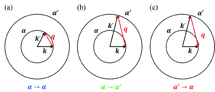
The functions are the transition rates between bands and (see Fig. 2) given by
| (4a) | |||||
| (4b) | |||||
| (4c) | |||||
where is a randomly distributed impurity density, is an angle between the incoming and outgoing wavevectors of and , and is the square of the wavefunction overlap. Here the cosine weight factors represent the contribution from parallel to while that perpendicular to is cancelled in the integration. Thus, by solving the coupled equations in Eq. (3) for multiband system, we can obtain the transport relaxation time for each band Siggia1970 ; Sarma1987 ; Breitkreiz2013 .
If we consider a single-band system, only the intraband transition term appears in Eq. (3), and becomes , i.e., the inverse of the one band momentum relaxation time, as in the well-known conventional relaxation time approximation Ashcroft . In contrast, in a multiband system, represents the interband transition rate, which describes the scattering from bands to , whereas describes the interband transition rate from the -th band scattered into the -th band, as schematically shown in Fig. 2. Note that have different cosine weight factors, which leads to a reduced or enhanced contribution depending on the scattering directions. The weight factor in Eq. (4c) arises from the velocity difference between bands and .
The current density induced by an electric field is
| (5) |
where and are spin and valley degeneracies, respectively, and is the conductivity tensor given by
| (6) |
Assuming an isotropic band structure with , at zero temperature we finally obtain
| (7) |
where is the DOS (per spin and valley) at the Fermi energy , and is the diffusion constant of the -th band, where and are the Fermi velocity and transport relaxation time, respectively, at .
In this work, we consider two types of scattering sources: long-range Coulomb scattering and short-range scattering. In general, the Coulomb scattering is known to be an important scattering mechanism at low densities, whereas the short-ranged scattering mechanism is believed to be important at high carrier densities Sarma2011 ; Min2011 . The charged impurities are screened by the carriers, and we treat the screened Coulomb potential within the Thomas-Fermi approximation, , where is the Thomas-Fermi wavevector, is the effective background dielectric constant, is the total DOS at the Fermi energy (which includes the spin and valley degeneracies as well as all the bands crossing ), and is the average distance between the impurities and the graphene sheet. The short-range scatterers describe atomic defects or vacancies, and can be approximated as a Dirac-delta function in the real space or a constant potential in the momentum space. When we consider both charged impurities and short-range scatterers together, we add their scattering rates according to Matthiessen’s rule, assuming that each scattering mechanism is independent.
From Eq. (7), we first qualitatively describe the conductivity behaviors of multilayer graphene when higher subbands are occupied by charge carriers. When the Fermi energy reaches the higher subbands, there are three notable features in the transport properties. First, the conducting channels increase because charge carriers in the high-energy subbands participate in transport, which provides higher conductivity. Second, the scattering channels are increased because of the allowed interband scatterings, which make the scattering rate increase (or equivalently, conductivity decreases). Third, the screening is enhanced because the DOS increases because of the higher band contribution, which reduces scattering and increases conductivity for charged impurities. The net effect of the conductivity change is determined by competition among these effects Lange1993 .
RESULTS AND DISCUSSION
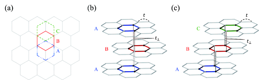
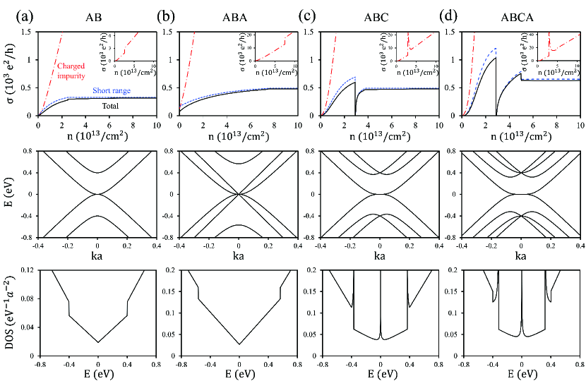
In this section, we show the calculated conductivity of multilayer graphene in terms of the carrier density. In the calculations, we used the following parameters to qualitatively match with known experimental data Morozov2008 ; Ye2011 : cm-2, , for charged impurities, and for short-range scatterers, (eV)2. For the tight-binding parameters, we used eV and eV for the nearest-neighbor intralayer and interlayer hopping terms, respectively, [see Fig. 1(b)] neglecting remote hopping terms for simplicity Min2008a ; Min2008b .
Figure 3 shows the numerically calculated conductivity as a function of carrier density for (a) AB bilayer, (b) ABA trilayer, (c) ABC trilayer, and (d) ABCA tetralayer graphene. A salient feature in our results is the conductivity drop at a certain carrier density ( cm-2), where the second subband begins to be occupied by charge carriers. The conductivity drop is especially prominent in ABC and ABCA stacking. In AB and ABA stacking, there is no significant change in conductivity at the bottom of the second subband, which can be attributed to the cancellation between the enhancement of interband scattering and the increase in conducting channels. We find that the conductivity drop is significant for the short-range scatterers, which are the dominant scattering source at high carrier densities. Thus, overall conductivity at high carrier densities follows the behavior of short-range scattering. When we consider only screened charged impurities, the conductivity shows a peak at the band touching point instead of a drop, which is mostly induced by the enhanced screening associated with the enhanced DOS.
To understand these opposite behaviors at the band touching density for the two scattering sources, we consider the DOS dependence of the scattering rate for each impurity. Note that , which negatively contributes to the scattering rate, is typically much smaller than because of the cosine weight factor in Eq. 4(c). The interband transition rate for the low-energy subband at the band touching point is then governed by the contribution from the low-energy subband to the high-energy subband, which is directly proportional to the higher band DOS, . Because is constant for short-range scatterers, the interband scattering rate becomes , leading to the conductivity drop. Thus, the conductivity drop is significant in the ABC and ABCA stackings because of the divergent DOS at the band touching point. For screened charged impurities, the screening effects play a more important role in the scattering rate, and we have (), where . Thus, the transition rate becomes approximately inversely proportional to the DOS, which decreases the overall transition rate. When the screening effect overwhelms the contribution from the interband transition in the scattering rate, the conductivity due to the charged impurities shows a peak at the band touching point. Because the scattering rates for short-range scatterers are much larger than those for charged impurities at the band touching point, the overall scattering rate of multilayer graphene is mainly governed by short-range scatterers and the total conductivity exhibits a drop at the band touching density. Note that at low carrier densities, the impurity scattering strongly depends on the stacking arrangements, whereas at high enough densities, multilayer graphene behaves as decoupled monolayer graphene sheets in which short-range scatterers dominate over charged impurities Min2011 .
The transport properties of the Bernal (periodic AB) and rhombohedral (periodic ABC) stacking arrangements are quite different because of the different electronic structures and chiral nature, even for the same number of layers, as shown in Fig. 3. In general, rhombohedral stacking shows a more pronounced conductivity drop near the band touching density than Bernal stacking. Although Bernal stacking is more stable and common, rhombohedral stacking is also found in highly ordered pyrolytic graphite or natural crystal graphite at a concentration of approximately Lui2011 , and thus can be used for novel device applications, as is discussed later.
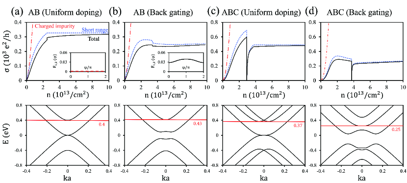
In most graphene-based field-effect transistors, the carrier density is controlled by gate voltage and the electronic band structure is affected by the applied gate voltage. We now consider the electrically gated multilayer graphene in which charge carriers are supplied from the back gate and the layer charge is determined electrostatically under the boundary condition that the electric field above the top layer is zero. Figures 4(a) and (b) show the conductivity of AB bilayer graphene. We compare the result obtained without the band modification (uniform doping) with the result obtained with the gate-voltage dependent band change (back gating). As shown in the insets of Figs. 4(a) and (b), the interband overlap factor in back-gated AB bilayer graphene does not vanish, in contrast to the uniform doping case, which enhances the interband scattering, leading to a conductivity drop at the band touching point. In the case of ABC trilayer graphene, the minimum of the second subband in the presence of the gating occurs near (but not exactly at because of the formation of a Mexican hat structure in the trilayer and beyond), which reduces the DOS. Thus, the conductivity drop becomes smaller than that of the uniform doping case, as shown in Figs. 4(c) and (d). These results indicate that the doping method affects the conductivity behavior at the bottom of the second subband by changing the energy band structure and its chiral nature.
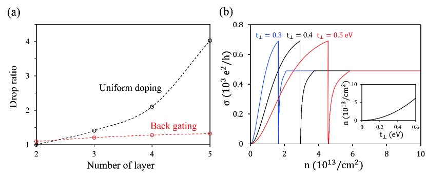
As discussed earlier, short-range scatterers are dominant over charged impurities at high carrier densities. In order to qualitatively understand the drop in conductivity, we focus on the density dependence of conductivity in the presence of dominant short-range scatterers only. We define the drop ratio as the ratio of conductivity just below the band touching density to that at cm-2. In Fig. 5(a), we show the conductivity drop ratio near the band touching point in rhombohedral stacking for uniform doping and back gating. The drop ratio increases with the number of layers because of the enhanced DOS at the band touching point. Note that the drop ratio for uniform doping is higher than that for back gating, which can be attributed to the occurrence of the band minima of the second subband away from , as shown in Figs. 4(c) and (d).
Figure 5(b) shows the density dependence of conductivity for short-range scatterers for several values of the interlayer hopping in ABC graphene. It is possible to control the band touching density by adjusting the interlayer hopping constant through the interlayer separation between layers. Note that the interlayer hopping with interlayer separation typically decays exponentially in the form of , where is the interlayer separation at which and is the characteristic decay length for the hopping integral Slater1954 ; Koshino2013 . We find that the conductivity value just before the band touching (, where is the lattice constant) and the saturation value at large carrier densities () do not depend on the interlayer hopping in the case of uniform doping. This means that a change in the interlayer hopping does not affect the drop ratio significantly, which is also true for back gating. As shown in the inset, however, the band touching density strongly depends on the interlayer hopping. Thus, the conductivity drop can occur at a much lower density if the interlayer separation is properly increased. We find that this trend is qualitatively true for a general rhombohedral graphene.
CONCLUSION
In summary, we studied the electronic transport properties of multilayer graphene, focusing on the effect of multiband scattering at high carrier densities where the higher subband is occupied by carriers. By directly solving the coupled Boltzmann transport equations in the presence of both charged Coulomb impurities and short-range scatterers, we showed that the conductivity of multilayer graphene exhibits a sudden change when charge carriers begin to occupy the higher subbands, and thus a large negative differential transconductance (NDTC) appears as the carrier density varies. The large NDTC arises mostly from the intersubband scattering and the change in the DOS at the band touching point. We found that the conductivity drop in rhombohedral stacking is more prominent than that in Bernal stacking because of divergent DOS at the bottom of the higher subbands and increased interband scatterings. We also showed that the conductivity drop is affected by the doping method and interlayer separation, and an efficient conductivity drop can be obtained for uniformly doped rhombohedral graphene. Based on our results, it may be possible to design novel devices utilizing the large NDTC in multilayer graphene in which the mean-free paths of the charge carriers are controlled by gating. In addition, the conductivity drop in multilayer graphene could be used for electronic device applications such as amplifiers, oscillators, and multivalued logic systems. For better device applications, we propose decreasing the band touching density by changing the interlayer separation and increasing the conductivity drop using uniform doping in rhombohedral stacking.
ACKNOWLEDGMENTS
This research was supported by Basic Science Research Program through the National Research Foundation of Korea (NRF) funded by the Ministry of Education under Grant No. 2015R1D1A1A01058071 (S.W. and H.M.) and 2017R1A2A2A05001403 (E.H.H.).
References
- (1) Raza H (Ed.) 2012 Graphene Nanoelectronics: Metrology, Synthesis, Properties and Applications; Springer: Berlin Heidelberg
- (2) McCann E and Fal’ko V I 2006 Phys. Rev. Lett. 96 086805
- (3) McCann E 2006 Phys. Rev. B 74 161403(R)
- (4) Min H, Sahu B, Banerjee S K and MacDonald A H 2007 Phys. Rev. B 75 155115
- (5) Min H and MacDonald A H 2008 Phys. Rev. B 77 77 155416
- (6) Min H and MacDonald A H 2008 Prog. Theor. Phys. Suppl. 176 227-252
- (7) Das Sarma S, Adam S, Hwang E H and Rossi E 2011 Rev. Mod. Phys. 83 407
- (8) Efetov D K, Maher P, Glinskis S and Kim P 2011 Phys. Rev. B 84 161412(R)
- (9) Ye J, Craciun M F, Koshino M, Russo S, Inoue S, Yuan H, Shimotani H, Morpurgo A F and Iwasa Y 2011 Proc. Natl. Acad. Sci. U.S.A. 108 13002-13006
- (10) Hwang E H, Adam S and Das Sarma S 2007 Phys. Rev. Lett 98 186806
- (11) Tan Y -W, Zhang Y, Bolotin K, Zhao Y, Adam S, Hwang E H, Das Sarma S, Stormer H L and Kim P 2007 Phys. Rev. Lett. 99 246803
- (12) Vaziri S, Lupina G, Henkel C, Smith A D, Östling M, Dabrowski J, Lippert G, Mehr W and Lemme M C 2013 Nano Lett. 13 1435-1439
- (13) Tse W -K, Hwang E H and Das Sarma S 2008 Appl. Phys. Lett. 93 023128
- (14) Sakamoto T, Kawamura H, Baba T and Iizuka T 2000 Appl. Phys. Lett. 76 2618
- (15) Palevski A, Heiblum M, Umbach C P, Knoedler C M, Broers A N and Koch R H 1989 Phys. Rev. Lett. 62 1776
- (16) Siggia E D and Kwok P C 1970 Phys. Rev. B 2 1024
- (17) Das Sarma S and Xie X C 1987 Phys. Rev. B 35 9875(R)
- (18) Breitkreiz M, Brydon P M R and Timm C 2013 Phys. Rev. B 88 085103
- (19) Ashcroft N W and Mermin N D 1976 Solid State Physics; Saunders: New York
- (20) Min H, Jain P, Adam S and Stiles M D 2011 Phys. Rev. B 83 195117
- (21) de Lange W, Blom F A P, van Hall P J, Koenraad P M and Wolter J H 1993 Physica B 184 216-220
- (22) Morozov S V, Novoselov K S, Katsnelson M I, Schedin F, Elias D C, Jaszczak J A and Geim A K 2008 Phys. Rev. Lett 100 016602
- (23) Lui C H, Li Z, Chen Z, Klimov P V, Brus L E and Heinz T F 2011 Nano Lett. 11 164-169
- (24) Slater J and Koster G 1954 Phys. Rev. 94 1498
- (25) Koshino M 2013 Phys. Rev. B 88 115409