A single electron transistor with quantum rings
Abstract
We Have developed the concept of a new kind of single-electron transistor in which the transport of the electron through a quantum wire is controlled by charged quantum rings. Using a 2D harmonic potential as the transverse constraint, we numerically investigated the transport of the electron through the wire. We have shown that in the low energy limit, for a suitable configuration of the rings, called the quadrupole configuration, we are able to adjust the conductance of the wire and therefore control the switching process.
pacs:
72.10.-d,73.63.-b,84.32.Dd,85.30.Mn,85.30.TvI INTRODUCTION
During the last decade there has been a growing interest for developing new electronic devices in nanoscales. The quantum behavior of these devices gives them new abilities never seen in classical electronics. A well-known example is the single electron transistor (SET). It is considered as an important element of future low power and high density integrated circuits. SET is a nanoscale switching device which is made of an electronic channel between the source and the drain and is based on the tunneling effect. A gate voltage is used to control a one-by-one electron transfer from the source to the drain via a quantum dot (QD). When the voltage is less than a threshold voltage , the system is in the Coulomb blockade state and the switch is closed. If the voltage exceeds , the switch is open and the current can start to flow through the channel. The goal of this paper is to introduce a new type of SET in which electronic transport in discrete channels of a quantum wire (which we call the transverse modes) is controlled by circular charged quantum rings. This may allow better control of the switching process compared to the usual SETs.
To implement the required configuration for this study, we have to utilize quantum wires and quantum rings. The Drude model describes the transport of electrons in conductors by the Boltzmann transport equation and introduces a mean free path . If the system’s dimensions are less than the mean free path , the impurity scattering is negligible. In this case, the electron transport can be regarded as truly ballistic (conducting without any scattering). At relatively low temperatures, the contribution to the conductance is given by the electrons with energies close to the Fermi surface . Quantum wires are defined as electrical conductors that have a thickness or diameter comparable with the Fermi wavelength or less, and a length less than . Therefore, the wire can be regarded as a quasi one-dimensional system in which the quantum effects influence the transport properties of the electrons. Typical quantum wires are tens of nanometers in diameter and a few micrometers in length. Due to their rich and fascinating electrical properties, the metallic nanowires are of particular interest Lin03 .
Let us consider a perfect quantum wire between two terminals. We assume the quantum wire is composed of a given number of transverse modes. According to the Büttiker model Buttiker , the electron dynamics in the effective mass approximation is described by the following Hamiltonian:
| (1) |
where is the effective mass of the electron, is a confining potential, is in the transverse direction and is the conduction band edge of the (bulk) conductor material. Because of the narrowness of the confining potential the energy for the transverse propagation is quantized (, is the index for the discrete spectrum). The total energy for each transverse mode can be written as
| (2) |
Here is the wave vector component along the wire.
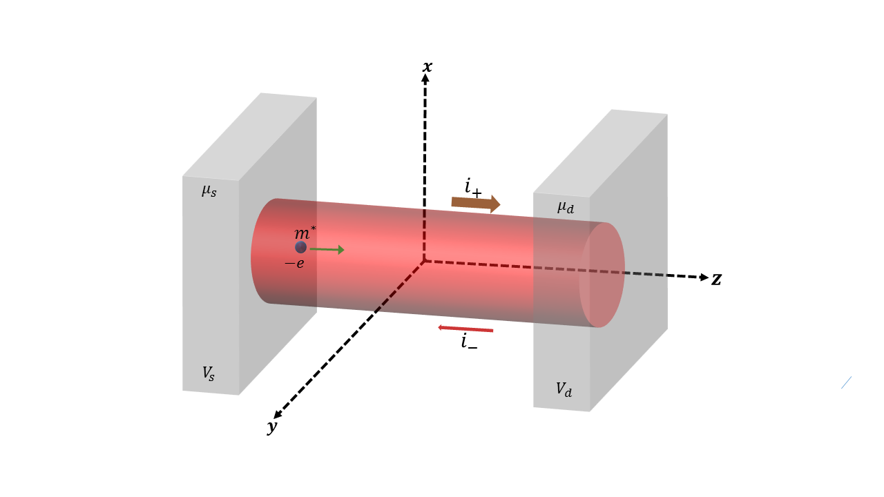
The electrons of a contact in thermodynamical equilibrium can be considered to be Fermi-distributed with an electrochemical potential . Assuming a quantum wire between two contacts with chemical potentials and (Fig.1), the net contribution to the conductance is from the electrons lying in the states with energy such that . In reality the potential landscape inside the device will be modified due to the electrostatic potential created by the electrons. However, for simplicity we assume that the chemical potential is constant for and inside the channel, and we do not have to consider any voltage drop inside the device. Besides we assume that the thermal energy is much smaller than the energy gap between the levels. In this case the conductance is given by Landauer
| (3) |
where the so-called von Klitzing constant is the standard resistance quantum and is the number of open channels of the quantum wire with an energy which is given by
| (4) |
So far we considered a perfect quantum wire i.e., without dissipation or scatterer. However, in the case of scattering induced by a scatterer (such as defects, impurities or irregularities) the conductivity, in temperature if a small bias voltage is applied to the system () is given by the Landauer equation
| (5) |
where the summation is over the open channels. Here denotes the probability of transition from the state to and is the Fermi-Dirac distribution function. is referred to as the broadening function. In zero temperature Eq.(5) is simplified to
| (6) |
which in the absence of scattering () is reduced to Eq.(3).
The other requirements for our configuration are quantum rings (QRs). QRs and QDs are two well-known examples of quasi-zero-dimensional structures. Because of their size which are of the order of phase-coherence length of their electrons, these structures exhibit some interesting purely quantum mechanical effects. The electronic states of these nano-size objects are quantized just like those of an atom. However, these so-called artificial atoms have the advantage that their electronics and optical behaviors are tunable and the engineered nature of them enables the adjusting of their properties in the fabricating process which makes them very useful. Zinc oxide nanorings, formed by rolling up single-crystal nano belts are well-known quantum rings Hughes . QRs can also be produced by droplet epitaxial growth Mano ; Kuroda and atomic force microscope tip oxidation Fuhrer ; Keyser techniques.
Due to their topology, QRs show more flexibility in electronic structure design compared to QDs. This allows better control of their physical properties than do QDs, by varying shape parameters such as ring width and outer-inner radius ratio. Moreover we can make coupling between electrons of the ring and a magnetic or a radiation field. It is also possible to grow QRs on photonic crystals or optical cavities. These abilities enable us to control behavior of the rings using quantum electrodynamical effects. The Aharanov-Bohm effect Aharanov ; Chambers is a well-known example which arises from the direct influence of the vector potential on the phase of the electron wave function. This results in the magnetic-flux-like splitting of electron energy levels corresponding to mutually opposite electronic rotationButtiker83 . As another example one can make coupling between electrons of the ring and circularly polarized photons which results in the magnetic-flux-like splitting of the electron energy levels Kibis and oscillations of the ring conductance as a function of the intensity and frequency of the irradiation Sigurdsson .
QRs can be coupled to each other in different configurations, result in the formation of the so called artificial molecules. Experimental realization Somaschini and theoretical consideration Chwiej ; Fuster ; Szafran ; Escartin ; Planelles ; Climente ; Climente2006 ; Malet ; Planelles2007 ; Culchac of coupled QRs with different configurations have been reported. The possibility to control the coupling between rings, their electron distribution, and electron transition from one ring to another have widely been considered for multiple quantum rings Kuroda ; Fuhrer ; Salehani ; Szafran ; Climente2006 ; Lorke2000 ; Keyser2002 ; Abbarchi ; Bayer ; Arsoski ; Filikhin1 ; Filikhin2 ; Aronov ; Chakraborty ; Lee ; Simonin ; Voskoboynikov ; Li ; Cui ; Sanguinetti ; Chena ; Szafran08 ; Zhu .
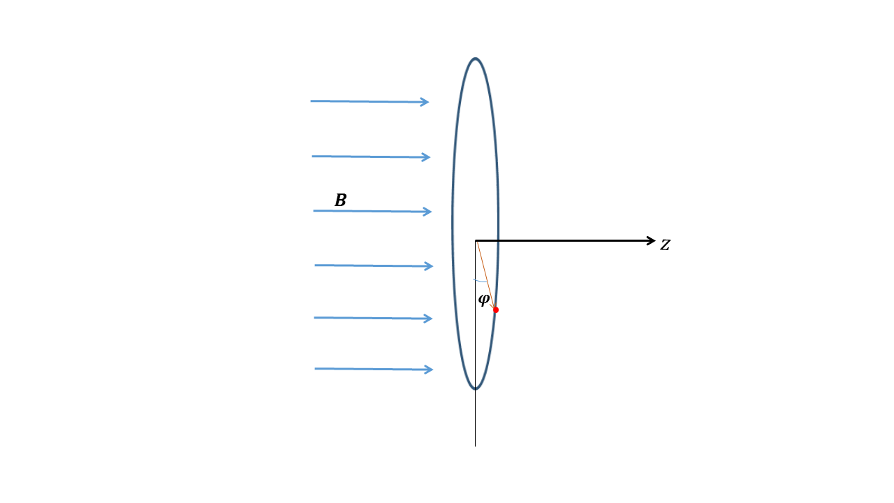
In a simple model we can assume a ring to be perfect and strictly one dimensional with radius pierced by a magnetic flux (Fig.2), and filled with spinless non-interacting electrons (only one particle per state). In the single mode regime the 1 particle Hamiltonian in cylindrical coordinates is given by
| (7) |
which has the solution
| (8) |
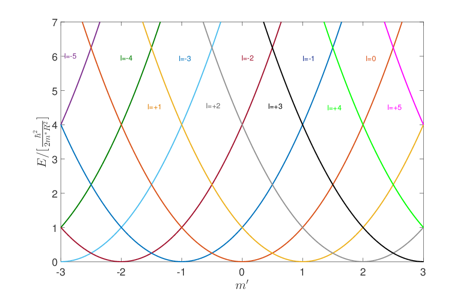
where ( Wb is the magnetic flux quantum) is the number of flux quanta penetrating the ring and is the angular momentum of the electron which is integer due to the boundary condition . The spectrum of this Hamiltonian has been shown in Fig.3. It consists of parabolas shifted with respect to each other by one flux quanta. Each parabola corresponds to a certain value of .
For electrons the (trivial) total energy and total angular momentum are
| (9) |
and
| (10) |
respectively. Here we assumed to be no Coulomb interaction between the electrons. However this interaction can be described by the capacitance of the system. Actually given a certain number of electrons the energy that it takes to overcome the Coulomb repulsion in order to bring one more electron is given by
| (11) |
where is the difference of the quantum levels of the system. The number of electrons on the ring can be tuned one by one (which is a practical requirement for our configuration of SET), e.g. by adjusting the voltages of the ring Ihn05 ; Ihn03 ; Xiang . Due to the Coulomb blockade, just at certain voltages (corresponding to constructive interference of the electron wave function, which results in high conductance of the ring), the provided energy is sufficient to compensate energy difference of the and many particle states in the ring and induce another electron on the ring Ihn03 .
II Our Model for SET
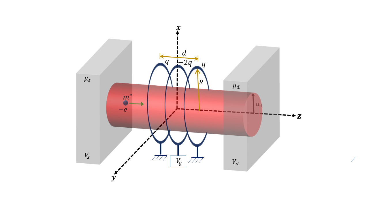
To expand our work more clearly, let us consider the schematic drawing of the configuration as shown in Fig.4: a moving electron passing through a quantum wire surrounded by a triple quantum ring (TQR). The TQR consists of three coaxial quantum rings acting as an electrostatic quadrupole and applying an external interaction potential on the electron. Assuming the charge distribution of the rings (q for the side rings and -2q for the inner ring) to be homogeneous for simplicity, some straightforward calculations for the interaction potential leads to Jackson
| (12) |
where , , and s are the Legendre polynomials. and are the radius and length of the TQR, respectively. We chose the 2D harmonic oscillator with frequency as the transverse constraint for the quantum wire. The related radius of the wire can be approximated as . is the effective mass of the electron. The electron moving through the wire feels two originally different potentials: the external interaction potential owing to the charged rings and the 2D harmonic potential of the confinement.
In the effective mass approximation the Schrödinger equation governing the motion of the electron with mass and energy , is
| (13) |
Here and are the longitudinal and transverse collision energies respectively. The radial and azimuthal quantum numbers and of the 2D harmonic oscillator independently takes the values and , respectively. Performing the scale transformation , , and (here is an arbitrary constant, and ; we assume that nm and ) leads to the scaled dimensionless Schrödinger equation
| (14) |
Due to the axial symmetry of the system, the angular momentum component along the z-axis () is conserved and one can separate the variable. Therefore the problem can be reduced to a 2D one. In the asymptotic region, , the electric potential (12) falls off as and thus it is negligible compared to other terms of the Hamiltonian. In this case the axial and transverse motions decouple (this is the reason why we use quadrupole instead of monopole or dipole configuration). Thus the quantum numbers and can be used to label the asymptotic states (channels) as , where s are the eigenfunctions of the 2D harmonic potential, and the momentum is defined as
| (15) |
with .
Assuming the electron to be initially in the channel , the asymptotic wave function (when ) takes the form
| (16) |
where s are the scattering amplitudes which describe transitions between the channels and . is the number of the open excited transverse channels, i.e. the maximum value of such that is real. The scattering amplitude depends also on . However, is conserved. Hereafter we assume .
Using the asymptotic wave function (16) one obtains for the inelastic transmission coefficient
| (17) |
where is the Heavyside step-function.
III Numerical Approach
To solve Eq.(14) we use the method introduced in Saeidian . First we discretize (14) on a grid of the angular variable with being the roots of and expand the solution as
| (18) |
where . In order for to be finite at the origin, we must have
| (19) |
The coefficients are defined as and is the inverse of the matrix with elements . s are the normalized Legendre Polynomials and s are the weights of the Gauss quadrature. By substituting (18) into (14) we arrive at a system of coupled equations
| (20) |
By mapping and discretizing onto the uniform grid according to , with (here is chosen in the asymptotic region , and is a tuning parameter) and using the finite difference approximation we solve the above system of equations with the boundary conditions (16) in a modified form (in which we eliminate the unknown coefficients ) and (19), for fixed colliding energy . By matching the calculated wave function with the asymptotic behavior (16) at , we find the scattering amplitudes from which we can calculate (see Eq.(17)).
IV Results
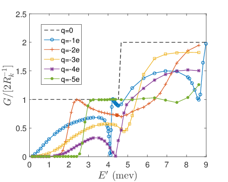
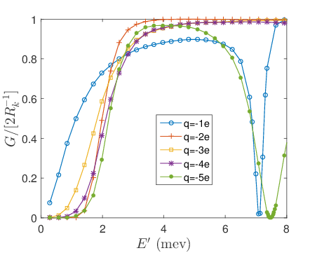
In Fig.5 we have depicted vs for up to two open channels for different values of . The results have been obtained for nm, nm and nm. It is obvious that increases as the number of open channels increases. However, there are some minimums which are due to the so-called confinement induced resonance (CIR). CIR was first studied for ultracold atoms in harmonic waveguides by M. Olshanii in 1998 Olshanii . He showed that CIR for s-wave scattering is a kind of the zero-energy Feshbach resonance. It occurs when the total energy of the incident particle in the confined geometry coincides with the energy of the quasi-bound state of the next excited channel. In this case the effective force experienced by the particle diverges and the transmission coefficient , reaches a minimum, which is zero in single mode regime (i.e. the particle is totally reflected). CIR has been studied for higher partial waves as well Granger ; Kim ; Saeidian ; Giannakeas . We observe the same effect in our problem: the confining potential induces a resonance which is responsible for minimization of the transmission coefficient .
We see from Fig.5 that for as well as , remains almost zero (no current) in a relatively wide range of (i.e., the switch is closed). With increasing , the conductance increases rather abruptly by 1 unit.
On the other hand, for fixed we can control the switching process by tuning the applied voltages of the rings (i.e., changing the charges of the rings).
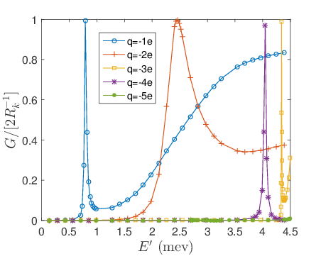
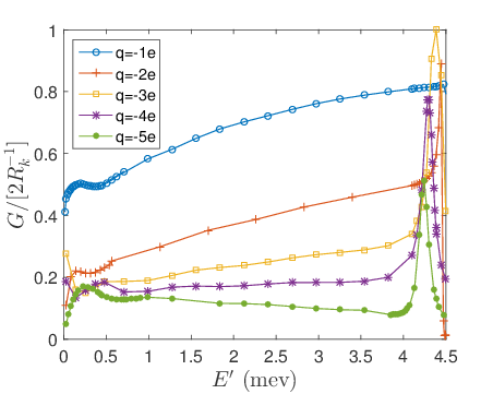
Fig.6 shows a graph of vs. in the one-mode regime. All the parameters in Fig.6 are the same as those in Fig.5 except for (nm) which is larger. There is a peak for each value of . However, is smaller on average compared with Fig.5. For and , is almost zero except for a sharp peak at large . This may allow us to measure small potential difference between the source and drain.
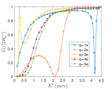
Figs.7 and 8 shows our results in single mode regime for the same parameters as those in Fig.5 but for larger (nm) and (nm), respectively. The conductance tends to increase when we increase the energy of the electron, remaining nearly constant in its maximum in a relatively wide range of . However it falls into zero rather abruptly in certain energies. Comparing these figures with Fig.5 shows dependence of the conductance on and . The larger or the smaller , the larger on average the conductance is.
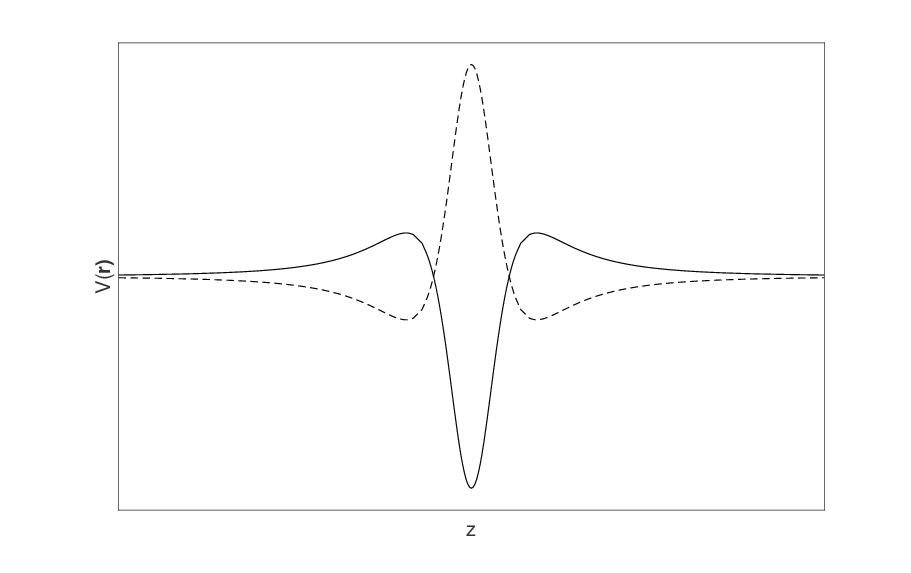
So far we have considered the case , i.e., the side rings have gained electrons while the inner ring has lost electrons. Fig.9 shows vs for the reverse case () for the same parameters as Fig.5. In this case changes very slowly as increases except for a sharp peak at large near to the next channel threshold. The peak shifts to the left as increases. The larger , the smaller on average the conductance is. This is because of the fact that for larger the moving electron experiences a stronger potential barrier (see Fig.10). The stronger the potential barrier, the less the probability of tunneling is.
To explain the dependence of on the sign of we have plotted a schematic diagram of the interaction potential along the -axis in Fig.10. The shape of the potential depends on the sign of . For there is a strong well between two weak barriers. The potential may support quasi-bound state leading to CIR. While for we see two shallow minimums separated by a strong potential barrier. The electron transmission is based on tunneling through this barrier.
V SUMMARY AND CONCLUSION
In summary, we have introduced a new kind of single electron transistor based on quadrupole configuration of quantum rings. With setting the charges of the rings, we can control conductance of the wire. Due to the Coulomb blockade, the charges of the rings can be changes just in specific voltages which can be engineered by applying magnetic field and/or circularly polarized light. This allows better control of the switching process compared to the usual single electron transistor based on quantum dots.
VI ACKNOWLEDGMENTS
Sh. S would like to thank A. Valizadeh and A. Ghorbanzadeh for fruitful discussions and S. Azizi for his contribution to the figures.
References
- (1) J. F. Lin, et al., Appl. Phys. Lett. 82, 802 (2003).
- (2) M. Büttiker, Phys. Rev. B 38, 9375 (1988).
- (3) R. Landauer, J. Phys.: Cond. Matter 1, 8099 (1989).
- (4) W. L. Hughes and Z. L. Wang, J. Am. Chem. Soc., 126 (21), 6703 (2004).
- (5) T. Mano, et al., Nano Lett. 5, 425-8 (2005).
- (6) T. Kuroda, et al., Phys. Rev. B 72, 205301 (2005).
- (7) A. Fuhrer, et al., Nature 413, 822-5 (2001).
- (8) U. F. Keyser, et al., Phys. Rev. Lett. 90, 196601 (2003).
- (9) Y. Aharanov and D. Bohm, Phys. Rev. 115, 485 (1959).
- (10) R. G. Chambers, Phys. Rev. Lett. 5, 3 (1960).
- (11) M. Büttiker, et al., Phys. Lett. A 96, 365 (1983).
- (12) O. V. Kibis, Phys. Rev. Lett. 107, 106802 (2011).
- (13) H. Sigurdsson, et al., Phys. Rev. B 90, 235413 (2014).
- (14) C. Somaschini, et al., Nano Lett. 910, 3419-24 (2009).
- (15) T. Chwiej and B. Szafran, Phys. Rev. B78, 245306 (2008).
- (16) G. Fuster, et al., Brazilian Journal of Physics 34 no. 2B, 666-69 (2004).
- (17) J. Planelles and J. I. Climente, Eur. Phys. J. B 48, 65-70 (2005).
- (18) J. I. Climente and J. Planelles, Phys. Rev. B 72, 155322 (2005).
- (19) F. Malet, et al., Phys. Rev. B 73, 245324 (2006).
- (20) J. Planelles, et al., Journal of Physics, Conference Series 61, 936-41 (2008).
- (21) F. J. Culchac, et al. Microelectronics Journal 39, 402-06 (2008).
- (22) J. M. Scartin, et al. Physica E 42, 841-3 (2010).
- (23) B. Szafran and F. M. Peeters, Phys. Rev. B 72, 155316 (2005).
- (24) J. I. Climente, et al., Phys. Rev. B 73, 235327 (2006).
- (25) H. K. Salehani, et al., Int. J. Nanoscience and Nanotechnology, vol 7 No. 2, 65 (2011).
- (26) A. Lorke et al., Phys. Rev. Lett. 84, 2223 (2000).
- (27) U. F. Keyser et al., Semocond. Sci. Technol. 17, L22 (2002).
- (28) M. Abbarchi, et al., Phyd. Rev. B 81 035334 (2010).
- (29) M. Bayer, et al., Phys. Rev. Lett. 90, 186801 (2003).
- (30) V. Arsoski, et al. Acta Physica Polonica 117, 733 (2010).
- (31) I. Filikhin, et al., Journal of Computational and Theoretical Nanoscience 9(8) · June 2011
- (32) I. Filikhin, et al., E: Low-dimensional Systems and Nanostructures 43, 1669 (2011).
- (33) A. G. Aronov and Yu. V. Sharvin, Rev. Mod. Phys. 59, 755 (1987).
- (34) T. Chakraborti and P. Pietilainen, Phys. Rev. B 50 8460 (1994).
- (35) B. C. Lee, et al., Physica E24, 87 (2004).
- (36) J. Simonin, et al., Phys. Rev. B 70, 205305 (2004).
- (37) O. Voskoboynikov, et al., Phys. Rev. B 66, 155306 (2002).
- (38) Y. Li, et al., Surf. Sci. 532, 811 (2003).
- (39) J. Cui, et al., Appl. Phys. Lett. 83, 2907 (2003).
- (40) S. Sanguinetti, et al., Phys. Rev. B 77, 125404 (2008).
- (41) G. -Y. Chena, et al., Solid State Communications 143, 515 (2007).
- (42) B. Szafran, Phys. Rev. B 77, 205313 (2008).
- (43) J. -L. Zhu, et al., Phys. Rev. B 72, 075411 (2005).
- (44) T. Ihn, et al., europhysics news PP 78-81 MAY/JUNE (2005).
- (45) T. Ihn, et al., Adv. in Solid State Phys. 43, pp. 139–154 (2003).
- (46) X. Y. Kong and Z. L. Wang, Nano Lett. Vol. 3, No. 12, 1625-1631 (2003).
- (47) J. D. Jackson, Classical Electrodynamics, WILEY, 3rd ed (1998).
- (48) S. Saeidian, V.S. Melezhik, and P. Schmelcher, Phys. Rev. A77, 042721 (2008).
- (49) M. Olshanii Phys. Rev. Lett. 81, 938 (1998).
- (50) B. E. Granger and D. Blume Phys. Rev. Lett. 92, 133202 (2004).
- (51) J. I. Kim, V.S. Melezhik, and P. Schmelcher, Phys. Rev. Lett.97, 193203 (2006).
- (52) P. Giannakeas, V.S. Melezhik, and P. Schmelcher, Phys. Rev. A84, 023618 (2011).