aff1]Institut für Astronomie und Astrophysik, Kepler Center for Astro and Particle Physics, Eberhard Karls Universität Tübingen, Sand 1, 72074 Tübingen, Germany aff2]Proc. SPIE 9145, Ground-based and Airborne Telescopes V, 914531 (22 July 2014) aff3]See www.cta-observatory.org for full author and affiliation list \corresp[cor1]Corresponding author: eisenkolb@astro.uni-tuebingen.de
An Efficient Test Facility For The Cherenkov Telescope Array FlashCam Readout Electronics Production
Abstract
The Cherenkov Telescope Array (CTA) is the planned next-generation instrument for ground-based gamma-ray astronomy, currently under preparation by a world-wide consortium. The FlashCam group is preparing a photomultiplier-based camera for the Medium Size Telescopes of CTA, with a fully digital Readout System (ROS). For the forthcoming mass production of a substantial number of cameras, efficient test routines for all components are currently under development. We report here on a test facility for the ROS components. A test setup and routines have been developed and an early version of that setup has successfully been used to test a significant fraction of the ROS for the FlashCam camera prototype in January 2016. The test setup with its components and interface, as well as first results, are presented here.
1 INTRODUCTION
FlashCam for Medium Size Telescopes (MST) is a photo-multiplier tube (PMT) based camera for Cherenkov telescopes. Its main distinctive features are the spatial separation between Photon Detection Plane (PDP) and Readout System (ROS), the use of a logarithmic amplifier to cover a large input signal range with only one channel, and a fully digital ROS. This means that the PMT signal is digitized directly after amplification, and that the trigger decision is made on digital data. This approach simplifies the analog electronics components of the camera. In 2016 a prototype camera with about half the number of pixels of a full FlashCam MST camera has been built and it is currently under severe testing at the Max-Planck-Institute for Nuclear Physics (MPIK) institute in Heidelberg. The current schedule foresees the fabrication of two pre-production cameras until 2018. To guarantee the highest reliability, all components of the ROS electronics (as well as all other components) will be tested, and their performance and functionality verified at the Institute for Astronomy and Astrophysics Tübingen (IAAT). To this end, a test facility has been designed whose devices and procedures were already used early in 2016 to test most of the ROS electronics for the FlashCam prototype and some more improvements have also been implemented for the application during pre-production and production.
![[Uncaptioned image]](/html/1610.04392/assets/Facilitylayout.png)
![[Uncaptioned image]](/html/1610.04392/assets/image.jpg) FIGURE 1. Sketch of the FlashCam ROS test-facility components.
FIGURE 2. The pulse generator designed at IAAT.
FIGURE 1. Sketch of the FlashCam ROS test-facility components.
FIGURE 2. The pulse generator designed at IAAT.
2 TEST FACILITY
The idea of the test facility is to quickly evaluate the functionality of the ROS electronics, independently of the Photon Detection Plane. The ROS consists of multi-purpose motherboards which can host one of three different kinds of daughter-boards. The first option is to mount two FADC daughter boards 111Flash Analog To Digital Converter. Daughter boards equipped with FADC chips to sample data at 250 MHz. for data sampling (up to 24 channels per motherboard). The second option is to mount one trigger daughter board to synchronize timing and distribute data between motherboards with FADC daughter boards (up to eight FADC equipped boards per trigger card). The third and last option is a master daughter board to do camera wide synchronization and trigger distribution and to interact with the telescope array.
The general layout of the facility is shown in Figure 1. Being able to evaluate the ROS independently of the PDP minimizes the complexity of the test environment. On one side, it minimizes the components involved, on the other side, it provides a known and easily controllable input to the ROS. To achieve this, the PDP is replaced by a combination of a pulse generator and a distribution/shaper board, which shapes the signal emitted by the pulse generator to closely resemble that of the FlashCam PDP. The pulse generator which was developed at IAAT is shown in Figure 2. It features eight channels with a maximum output amplitude of 3.5 V and a resolution of 10 bits. The rise time of two nanoseconds is critical for the shaped pulse to closely resemble that of the original PDP. To cover the whole signal range with sufficient accuracy an additional 20 dB attenuator can be switched in. The pulse generator can be interfaced via USB and an alternative serial connection via RS232 is currently being implemented. The goal of this development is to be independent of any software or drivers installed on lab PCs. The pulse generator provides a trigger output. The possibility to trigger the pulse generator externally is currently under development. A workstation running CentOS is used to control the pulse generator and it also works as an interface to the FlashCam ROS. The pulses emitted by the pulse generator, sketched in Figure 1, are sent to a pair of distribution and shaper boards developed at MPIK.
The basic idea is to have a signal with a very short rise time (smaller than several nanoseconds) and differentiate it. The resulting signal will have an approximate duration of that of the rising edge of the original signal and resemble in shape that of a PMT.
This PMT-like pulse is then shaped by an electronics circuit that resembles that of the preamplifier in the PDP of FlashCam. Both differentiation and shaping are done by the shaper board. The shaped pulses are then sent to FlashCam FADC boards, where they are digitized and stored in a ring buffer. This ring buffer can then be read out via a microblaze microcontroller inside the Spartan 6 FPGA on board of the FlashCam motherboards and it is then transmitted to the lab workstation.
All programmable options, such as the ADC baseline, can be set and tested, as well as signals with different amplitudes can be applied, read out and evaluated to cover the whole dynamic range. Higher level parameters such as the linearity of the reconstructed amplitude and the stability of the timing are analyzed automatically.
The measured data is then analyzed. First of all concerning the amplitudes a linear behavior is expected, thus a linear fit is applied and a verification on the fit parameters is applied to check if they are inside the specifications. For data that is not analytic, such as the full width at half maximum of the original pulse or center of gravity of the time derivative of the signal (which is used for timing), min/max curves are defined and it is checked whether the data falls into the defined regime.
More detailed electronics tests are only performed if the functionality tests fail. Then the boards are closely evaluated to find the cause of error, to give precise feedback to the manufacturer, and, if possible, fix the electronics in house.
The FlashCam ROS has two interface options. On a single board level connections can be made via RS232 interface or via raw Ethernet, which is a custom low level Ethernet protocol. The serial connection can be used to verify low level functionality whereas the raw Ethernet connection is used for normal operation and data transfer. Control of the test environment can happen either very directly via command line tools, alternatively a GUI gives a higher level interface and automates most of the test control.
The procedures for temperature and vibration tests is currently under evaluation. These are particularly interesting because they show dormant faults that may only occur later in a products lifetime, such as cold solders. Currently we plan to do temperature cycling over the storage temperature range for powered off devices as well as cycling over the operational range with powered devices. Exact specifications for these tests are currently being defined. Temperature cycling is favored over dedicated burn-in at the module level (see Scheiber [1, chap. 7] for details).
3 RESULTS FROM FIRST PROTOTYPE TESTS AND OUTLOOK
In January, a first version of the setup has been used at MPIK to test almost the complete ROS electronics for the FlashCam prototype. This included 104 motherboards and 140 FADC daughterboards, which corresponds to 1680 channels.
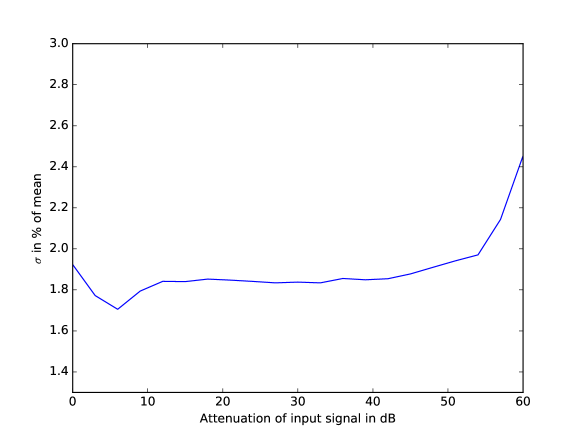
The tasks performed included the final assembly of the motherboards, optical inspection, configuration of the single boards as well as running the complete test suite. This verified the correct functionality of the ROS components, including configuration and event reconstruction with the required performance. Only a small number of components showed faults that were already identified in the first steps of configuration. Besides functionality and quality control and verification this test provided valuable input for the planned automation of evaluation of the test results. Figure 3 shows an example result. It shows the spread of the amplitudes at different input amplitudes over all motherboards. This has been done without cross calibration between the different boards. This shows again the functionality and stability of the FlashCam concept. The automated evaluation and control of the tests has since then been implemented. Currently the exact failure conditions and tolerances are being specified and the test facility is being prepared for future test runs. The inclusion of temperature cycling and vibration tests is being evaluated and the requirements for temperature cycling are finalized.
4 ACKNOWLEDGMENTS
We gratefully acknowledge support from the agencies and organizations under Funding Agencies at www.cta-observatory.org
References
- Scheiber [2001] S. F. Scheiber, “Environmental stress screening,” in Building a Successful Board-Test Strategy (Second Edition) (Butterworth-Heinemann, 2001) , pp. 202–206.