Automatic Generation of Equivalent Electrothermal SPICE Netlists from 3D Electrothermal Field Models
Abstract
Starting from a 3D electrothermal field problem discretized by the Finite Integration Technique, the equivalence to a circuit description is shown by exploiting the analogy to the Modified Nodal Analysis approach. Using this analogy, an algorithm for the automatic generation of a monolithic SPICE netlist is presented. Joule losses from the electrical circuit are included as heat sources in the thermal circuit. The thermal simulation yields nodal temperatures that influence the electrical conductivity. Apart from the used field discretization, this approach applies no further simplifications. An example 3D chip package is used to validate the algorithm.
I Introduction
For many electrothermal applications, complex problems need to be solved to calculate the desired quantities of interest. While analytical methods only serve for very simple problems, real world problems require numerical field simulations. Nowadays, Finite Difference (FD), Finite Element (FE) or Finite Volume (FV) methods are well known and frequently applied. On the other hand, when a fast computation is required, it is often recommended to derive a model that only consists of a few lumped elements which allows to use circuit simulators. However, network models are not always sufficiently accurate or they are too complex to be generated by hand compared to models based on partial differential equations. This paper attempts to fill this gap by deriving a circuit netlist from a field model, thereby avoiding any further approximation.
When the first circuit simulators were introduced, the Simulation Program with Integrated Circuit Emphasis (SPICE) soon became the standard tool for describing and solving circuits using netlists. At that time, the operating temperature of the simulated devices was set globally and did not change according to the operational load of the circuit. However, especially in power electronic applications that involve strongly temperature dependent materials [1, 2], self-heating and thermal coupling between devices become important and therefore the device’s temperature changes dynamically. Thus, the concurrent simulation of electrical and thermal circuits was soon developed as a SPICE extension [3]. To account for the coupling, an extra temperature node was added to the electrical device models [4, 5].
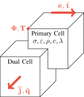
Traditionally, the circuit topology and the netlist parameters are determined by hand calculations which necessarily neglect nonlinear effects and field inhomogeneities. Nowadays, the thermal behavior is more accurately analyzed by 3D field solvers which allow to couple the resulting temperature distribution iteratively to the electric circuit simulator, known as the relaxation method [6, 7, 8]. On the other hand, the definition of mesh-based equivalent thermal circuits [9] motivates the direct method that couples the electrical and thermal circuits without any 3D field solver required. Following the direct approach, this work aims at exploiting the accurate electrothermal field model by automatic and loss-free extraction of an equivalent electrothermal circuit model (as visualized in Fig. 1). The netlists generated by this approach are therefore an exact representation of the nonlinear FD, FE or FV field discretizations. Moreover, a straightforward coupling with an additional (external) SPICE circuitry is possible and standard techniques of model order reduction for networks [10] can be applied afterwards.
If a 3D electrothermal field model is investigated, occasionally surrounding circuitry is treated by a field-circuit coupled approach [11, 12]. In some cases, a two-step procedure is executed, i.e., from the field model part, a reduced model is extracted and then included in a circuit model [13]. In this paper, a further alternative is proposed, i.e., the full field model is translated into a circuit model. This approach is promising for small device parts with severe electrothermal issues, to be embedded in an overall circuit model.
The paper is organized as follows: The electrothermal field problem is introduced in section II. Then, section III presents the discretization by the Finite Integration Technique (FIT). This technique is based on integral-type degrees of freedom and therefore allows a straightforward circuit interpretation as demonstrated in section IV. The details of the automatic SPICE netlist generation are given in section V. Finally, numeric validation examples are discussed in section VI before section VII concludes the paper.
II Electrothermal Field Problem
We consider an electrothermal problem that couples the electroquasistatic approximation of Maxwell’s equations [14] with the transient nonlinear heat equation
| (1) | ||||
| (2) |
subject to adequate initial and boundary conditions. The given quantities are the Joule heating term , the time , the temperature and the electric scalar potential . The material parameters , , , and are the electrical permittivity and conductivity, the thermal conductivity, the volumetric mass density and the specific heat capacity, respectively. All involved materials may be nonlinear, inhomogeneous or anisotropic. Note that the spatial dependencies have been suppressed here and that the temperature dependency of and is neglected.
III Discretization by the Finite Integration Technique
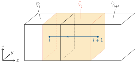
The coupled electrothermal problem given by (1) and (2) is discretized in space by the Finite Integration Technique (FIT) on a staggered 3D hexahedral grid with canonically indexed nodes [15, 16, 17]. The discretization turns the material relations and the differential operators into material matrices and topological matrices, respectively. The discrete unknowns, i.e., the electric potentials and the temperatures are associated with the nodes of the primary grid (see Fig. 2). The voltage and temperature drops are allocated at the primary edges and resemble differences, i.e., and , where is the discrete gradient matrix according to the topology of the primary grid. Electrical currents and heat fluxes are assigned to the facets of the dual grid. They are accumulated on the dual cells by and where is the discrete divergence matrix determined by the topology of the dual grid. The duality of the staggered grid gives raise to the property .
Note that the signs of the different entries of (and thus also ) define the orientation of the grid’s edges. Here, their direction is chosen to be the same as the direction of the coordinate axes. The sub-matrices with are therefore the discrete representation of the spatial derivatives , and . This results in entries on the main diagonals of and in entries on one of the super-diagonals. The discrete gradient matrix resembles an incidence matrix as used in circuit theory that is more structured than a typical circuit incidence matrix. Both matrices share the property that their column sums are zero.
The discrete unknowns at the primary grid are related to the ones at the dual grid by material matrices, i.e., the electrical conductance matrix , the electrical capacitance matrix , the thermal conductance matrix and the thermal capacitance matrix . The electrical currents, displacement currents, heat fluxes and stored heats are then given by
respectively. In case of a mutually orthogonal grid pair, the material matrices are diagonal. Then, each primary edge crosses the corresponding dual facet perpendicularly. The primary edge and facet as well as the primary nodes and dual cells are indexed pairwise identically. This gives the entries of , , and as
where is the length of the primary edge , is the area of the dual facet and is the volume of dual cell . The material parameters , , and are found by averaging the corresponding parameters, cf. [18, 19]. Note that the counter addresses all primary nodes (or dual volumes) while addresses all primary edges (or dual facets).
The applied averaging scheme depends on the allocation of the materials on the grid. In this paper, the material properties are allocated at the primary grid cells, i.e., each primary cell contains a homogeneous material. This gives rise to the so-called staircase approximation. Although this paper adopts this approximation for reasons of conciseness, partially filled cells [20] and conforming techniques [21] are preferred. According to the chosen allocation scheme (see Fig. 2), the averaging of a conductance for a primary-edge, dual-facet pair involves four surrounding primary volumes resulting in the average of the four involved conductivities. For an equidistant grid, this gives
| (3) |
with being a local counter over the four primary volumes that share the edge . Note that this averaging scheme can easily be generalized for non-equidistant grids by taking the different cell sizes into account.
The heat powers generated by the thermal losses from the electroquasistatic problem are calculated by
with the component-wise Hadamard product and the vector that allocates the thermal losses at the shifted cells with the volume as shown in Fig. 3. The shifted cells consist of two half dual cells sharing a common dual facet and are indexed according to the dual facets.
To include all calculated heat contributions as sources in the heat equation, they need to be integrated from the shifted volumes to the neighboring dual cells . This relation is given by
where is a local counter that loops over all shifted cells that intersect the dual cell . To sum up all contributions of the shifted volumes to the dual cell , the incidence matrix is defined. Then, the Joule losses on the dual cells become
| (4) |
Here, and are diagonal matrices containing the dual volumes and the shifted volumes , respectively.
Finally, the topological operators where , the material matrices , , and and the heat powers are utilized to express the discrete counterpart of (1) and (2), i.e.,
| (5) | ||||
| (6) |
The degrees of freedom are the discrete temperature vector and the electric potential vector . For both the electric and thermal part of the system, adequate initial and boundary conditions need to be defined. As stated here, (5) includes the definition of homogeneous Dirichlet boundary nodes while (6) is subject to homogeneous Neumann (adiabatic) conditions throughout this paper. Subsequently, the time is discretized by any standard scheme, e.g. the backward Euler method.
IV Circuit Theory
The equivalence between the discretized FIT formulations (5) and (6) and the Modified Nodal Analysis (MNA) [22, 23] becomes obvious when the latter is derived from the Maxwell equations along a similar reasoning as in section III. First, Kirchhoff’s Voltage Law (KVL) and Kirchhoff’s Current Law (KCL) are derived directly from Faraday’s law and the current continuity equation, respectively. Then, they are assembled together with the branch relations to give a circuit formulation. From this, the electric and thermal equivalences to the FIT formulation are obtained.
IV-A Kirchhoff’s Voltage Law (KVL)
In the electroquasistatic case, Faraday’s law reads
where is the surface enclosed by the loop such that , with branches . Loops in a circuit closely resemble loops in the primary grids, i.e., a loop is a collection of edges and nodes forming a closed path. The integral form of Faraday’s law directly breaks down in an addition of voltage drops along the branches giving
| (7) |
In MNA, (7) is implicitly fulfilled by defining the nodal voltages and expressing the branch voltages by
where is the circuit incidence matrix. In analogy to the FIT matrix (cf. section III), the entries of have to be subject to a convention. Let us define if branch is directed away from node and if branch is directed towards node . If branch is not directly connected to node , the corresponding entry is zero. The nodal voltages are the circuit counterpart of the electric potentials in the FIT formulation. Note that in the electrical case, at least one of the potentials needs to be chosen as the reference potential (ground) to ensure uniqueness of the solution.
IV-B Kirchhoff’s Current Law (KCL)
The KCL is derived from the current continuity equation
| (8) |
where is the charge density and an arbitrary cell. In analogy to FIT, we consider a cell around a node of the circuit. Furthermore, we assume that the total charge in is zero. This means that capacitive charges are located on branches that are either fully outside or fully inside . Then, (8) becomes
with the boundary of . Assuming that a finite number of conductors with cross-sectional areas and currents are leaving this cell, KCL is obtained as
Using the definition of the circuit incidence matrix,
states KCL for every node in the network. Note that denotes a vector of zeros of suitable dimension.
IV-C Branch Relations
Due to the nature of the considered problem, we limit ourselves to resistances, capacitances and current sources as branch elements. With resistive branches, capacitive branches and current sources, can be divided into different blocks representing these elements [23]. We therefore obtain
where , and . The vector of currents is partitioned accordingly, i.e.,
with the blocks , and . Similarly, with , and , the branch voltage vector is partitioned as
With these definitions, KVL and KCL are expressed by
| (9) | |||
| (10) |
The introduction of the diagonal conductance matrix and the diagonal capacitance matrix with the corresponding values on the diagonal leads to the branch relations
where is an arbitrary source current.
The combination of KVL, KCL and the branch relations gives the MNA formulation
| (11) |
IV-D Circuit Formulation and Electrical Equivalences
For the EQS case, when comparing the structure of (5) and (6) with (11), many equivalences are found. Thanks to the equally chosen orientation of the edges in the FIT grid in comparison to the edges in the MNA, the discrete field formulation can be interpreted as a circuit formulation by setting
| (12) | ||||
with the superscript denoting the quantities for the electroquasistatic case.
IV-E Thermal Circuit and Equivalences
In a thermal circuit, heat capacitances connect the circuit nodes to a common node (thermal ground) with zero temperature. This reflects the different nature of the term in (6) compared to the term in (5).
With node as the thermal ground node, (11) becomes
| (13) |
with , , and being the expansion of the corresponding quantities by this additional node. To mirror the structure of the discretized heat equation (6), we set the potential of the thermal ground node to zero and choose
Here, is the identity matrix and is a vector of ones with dimension . If we then omit line in (13) (as we would do with a ground node in an electric circuit), we end up with (11) again and obtain
| (14) | ||||
with the superscript denoting the quantities for the thermal problem.
The equivalences between the FIT formulation (5) and (6) and the circuit formulation (11) as shown above are the main motivation for this paper. The relations (12) and (14) allow to derive an equivalent SPICE netlist from any given 3D problem discretized by the FIT. The detailed methodology and numerical examples are discussed in the remaining sections of the paper.
V SPICE Netlist Generation
This section deals with the implementation details for the automated netlist generation. First, the topology of the generated network is described for the EQS problem including the extraction of the Joule loss term. Then, the topology of the thermal network with inclusion of the Joule loss term is discussed. In the second part of the section, the approach for nonlinear material relations is shown.
V-A Circuit Topology
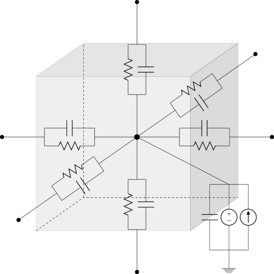
For the EQS problem, the degrees of freedom in the FIT are the potentials allocated at the primary nodes. In the MNA, these potentials are placed on the nodes of the network and thus remain nodal values. From the previous section, we know that the branch voltages of capacitive and resistive branches are equal, cf. (9) and (12). Therefore, these elements are placed in parallel. With the definition of the voltages as the difference of two nodal potentials, the resistive and capacitive elements are located on the branches between the nodes. From the pair-wise equality of and as well as and , the entries and from the material matrices are the values for the lumped conductances and capacitances on circuit branch , respectively. To impose inhomogeneous Dirichlet boundaries, voltage sources between a Dirichlet node and ground have to be defined. Fig. 4(a) shows the structure of the described electrical circuit for one example branch between nodes and .
Since each branch contains resistive elements, the thermal losses need to be calculated on every branch. For branch , this is achieved by the evaluation of the branch voltage and the current giving
Note that this thermal power coincides with the one calculated in the field model discussed in section II. Writing the different in a vector, it becomes and leads to the thermal power on the dual volumes as given by (4).
For the thermal problem, the structure of the conductive part () is equal to the structure of the electrical problem. Therefore, as done for the electrical problem, conductive elements are placed on the branches between two circuit nodes. On the other hand, the structure of the capacitive part () differs slightly from the EQS structure. Since the identity matrix is chosen for the incidence matrix of the capacitive branches (), the voltage is not defined by temperature differences but by the absolute values of the temperatures (with respect to a reference temperature). If the temperature values are now allocated at the nodes of the thermal network, a capacitive connection from every thermal network node to the thermal ground as introduced in section IV is obtained. The values for these capacitances correspond to the values on the diagonal of , cf. (14). To include inhomogeneous Dirichlet conditions, temperature sources are modeled by voltage sources between the Dirichlet nodes and ground as done for the electrical circuit. Furthermore, the mapping of the heat powers to a circuit definition is given by its incidence matrix . Therefore, the corresponding current sources are placed between each circuit node and thermal ground. In Fig. 4(b), these observations are summarized for a thermal example edge.


V-B Nonlinear Materials
In practice, all material properties may depend on the temperature. In this section, the dominating nonlinearity is assumed to be the electric conductivity . However, other dependencies can be incorporated analogously. If an inhomogeneous material distribution is given in the domain of interest, the average conductivity has to be found as presented in section II. To correctly consider the nonlinearity in SPICE, this averaging needs to be carried out at runtime in the circuit solver. Therefore, a netlist with nonlinear entries is the result.
If we consider the average temperature of an edge , the conductivity of the surrounding primary cells needs to be evaluated according to its nonlinear definition. In the simplest case, the temperature dependence of an isotropic conductivity is expressed via the resistivity, i.e.,
In this equation, is the resistivity at the reference temperature and the temperature coefficient depending on the material of cell . Once the nonlinear functions have been evaluated, the average conductivity of edge can be found as given by (3). Then, the nonlinear conductance is established by the length of primary edge and the area of dual facet , giving
Note that more complex material laws, non-equidistant grids and a more sophisticated averaging can be implemented analogously.
A pseudocode for the generation of electrothermal netlists with nonlinearities is shown in Algorithm 1.
VI Numerical Validation
VI-A Benchmark Example
For validation of the presented methodology, a benchmark cuboid of dimensions is selected. It is composed of two different regions as shown in Fig. 5. The left part of length is chosen to be mainly resistive while the right part of length is mainly capacitive. The material properties of the two regions are summarized in Table I. On the boundaries in -direction, Perfect Electric Conducting (PEC) facets are assumed. At the left boundary, a sinusoidal electric Dirichlet condition with amplitude and a frequency of is imposed. At the right boundary, a potential of is applied. Homogeneous Neumann conditions are chosen for the remaining boundaries. Thermally, all boundaries are set to homogeneous Neumann (thus adiabatic) conditions. For the initial conditions, all electric and thermal non-Dirichlet nodes are set to zero.
| Property | ||
|---|---|---|
| 8000 | 8000 |
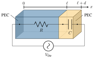
From a circuit point of view, the electric Dirichlet condition is modeled by a voltage source as the potential difference between the facets. Furthermore, the resistive material is modeled by a single resistance and the capacitive material by a single capacitor. However, the thermal properties of the two materials are assumed to be equal.
After setting up the model with its material properties and boundary conditions, Algorithm 1 generates an equivalent electrothermal netlist. Then, using this netlist, a SPICE simulation is carried out and compared with the electrothermal FIT simulation. The electrical simulation result is shown in Fig. 6. From the obtained potentials , the thermal loss term is calculated. These losses are then coupled into the heat equation yielding the resulting temperatures as shown in Fig. 7.
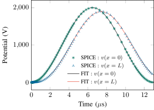
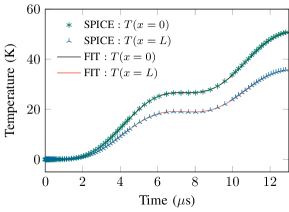
From all three figures, it is clearly seen that a very good agreement of the SPICE and FIT simulation is achieved. The relative error norm for the obtained temperature is calculated as
| (15) |
where and are vectors of dimension with being the number of time steps. Since the spatial discretization is chosen identically and the generated netlist is a representation of the 3D field model without any further simplifications, the only error is resulting from the different time integrators.
VI-B Chip Package
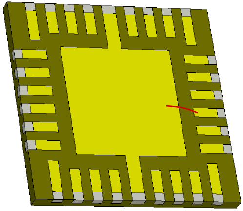
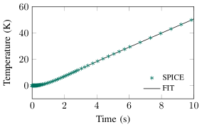
To apply the method to a more complex example, a microelectronic chip package as shown in Fig. 8 is considered. Here, the same setting as in [19] is chosen. However, only one bonding wire connects one of the contacts to the chip. The bonding wire’s electrical conductance is and its thermal conductance . Furthermore, the relative permittivity for all materials are set to one while the thermal boundary conditions are adiabatic. To excite the system, an exponential voltage is applied over the bonding wire. Algorithm 1 is executed to generate the equivalent netlist. This is simulated using SPICE and the temperature of the hottest node of the domain is compared to the result obtained by FIT as shown in Fig. 9. The error as calculated by (15) is . Due to the mainly resistive character of this example, the resulting constant current leads to a constant heating of the considered node.
VII Conclusions
The automatic generation of netlists directly from an electrothermal 3D field model has been presented. Starting from a Finite Integration Technique (FIT) discretization, an equivalent circuit description in terms of the Modified Nodal Analysis (MNA) was shown for the electrical as well as for the thermal case. As it is a direct representation of the field model, no further simplifications apply when generating the netlist. For validation, the field solution of an electrothermal benchmark example and a complex 3D chip package problem have been compared to the SPICE solution based on the generated netlist.
Next steps are the treatment of non-hexahedral meshes, arbitrary nonlinear materials and model order reduction of the resulting network to reduce the complexity of the obtained circuit and thus enable a more efficient circuit simulation.
VIII Acknowledgement
The authors thank Abdul Moiz for his passionate work during the first implementation of the algorithm for the automatic netlist generation. The work is supported by the European Union within FP7-ICT-2013 in the context of the Nano-electronic COupled Problems Solutions (nanoCOPS) project (grant no. 619166), by the Excellence Initiative of the German Federal and State Governments and the Graduate School of CE at TU Darmstadt.
References
- [1] M. März and P. Nance. Thermal modeling of power-electronic systems, 2000.
- [2] V. Košel, R. Illing, M. Glavanovics, and A. Šatka. Non-linear thermal modeling of DMOS transistor and validation using electrical measurements and FEM simulations. Microelectron. J., 41(12):889–896, December 2010.
- [3] R.S. Vogelsong and C. Brzezinski. Extending SPICE for electro-thermal simulation. In Proceedings of the IEEE 1989 Custom Integrated Circuits Conference, pages 21.4/1–21.4/4, May 1989.
- [4] P.A. Mawby, P.M. Igic, and M.S. Towers. New physics-based compact electro-thermal model of power diode dedicated to circuit simulation. In Proceedings IEEE Circuits and Systems ISCAS, volume 3, pages 401–404, May 2001.
- [5] A.R. Hefner and D.L. Blackburn. Thermal component models for electrothermal network simulation. IEEE Trans. Compon. Packag. Manuf., 17(3):413–424, September 1994.
- [6] W. van Petegem, B. Geeraerts, W. Sansen, and B. Graindourze. Electrothermal simulation and design of integrated circuits. IEEEJSolidStateCirc, 29(2):143–146, February 1994.
- [7] A. Chvala, D. Donoval, J. Marek, P. Pribytny, M. Molnar, and M. Mikolasek. Fast 3-D electrothermal device/circuit simulation of power superjunction MOSFET based on sdevice and HSPICE interaction. IEEE Trans. Electron. Dev., 61(4):1116–1122, April 2014.
- [8] S. Wunsche, C. Clauss, P. Schwarz, and F. Winkler. Electro-thermal circuit simulation using simulator coupling. IEEE Trans. Very Large Scale Integr. (VLSI) Syst., 5(3):277–282, September 1997.
- [9] N. Simpson, R. Wrobel, and P.H. Mellor. An accurate mesh-based equivalent circuit approach to thermal modeling. IEEE Trans. Magn., 50(2):269–272, February 2014.
- [10] M. Hinze, M. Kunkel, and U. Matthes. POD model order reduction of electrical networks with semiconductors modeled by the transient drift-diffusion equations. In Michael Günther, Andreas Bartel, Markus Brunk, Sebastian Schöps, and Michael Striebel, editors, Progress in Industrial Mathematics at ECMI 2010, volume 17 of Mathematics in Industry, Berlin, April 2012. Springer.
- [11] G. Benderskaya, H. De Gersem, T. Weiland, and M. Clemens. Transient field-circuit coupled formulation based on the finite integration technique and a mixed circuit formulation. COMPEL, 23(4):968–976, 2004.
- [12] S. Schöps, H. De Gersem, and T. Weiland. Winding functions in transient magnetoquasistatic field-circuit coupled simulations. COMPEL, 32(6):2063–2083, September 2013.
- [13] T. Wittig, I. Munteanu, R. Schuhmann, and T. Weiland. Model order reduction and equivalent circuit extraction for FIT discretized electromagnetic systems. Int. J. Numer. Model. Electron. Network. Dev. Field, 15(5-6):517–533, December 2002.
- [14] M. Clemens, M. Wilke, G. Benderskaya, H. De Gersem, W. Koch, and T. Weiland. Transient electro-quasistatic adaptive simulation schemes. IEEE Trans. Magn., 40(2):1294–1297, March 2004.
- [15] T. Weiland. A discretization method for the solution of Maxwell’s equations for six-component fields. AEU, 31:116–120, March 1977.
- [16] T. Weiland. Time domain electromagnetic field computation with finite difference methods. Int. J. Numer. Model. Electron. Network. Dev. Field, 9(4):295–319, 1996.
- [17] M. Clemens, E. Gjonaj, P. Pinder, and T. Weiland. Self-consistent simulations of transient heating effects in electrical devices using the Finite Integration Technique. IEEE Trans. Magn., 37(5):3375–3379, September 2001.
- [18] M. Clemens and T. Weiland. Discrete electromagnetism with the Finite Integration Technique. PIER, 32:65–87, 2001.
- [19] T. Casper, H. De Gersem, R. Gillon, T. Gotthans, T. Kratochvil, P. Meuris, and S. Schöps. Electrothermal simulation of bonding wire degradation under uncertain geometries. In Luca Fanucci and Jürgen Teich, editors, Proceedings of the 2016 Design, Automation & Test in Europe Conference & Exhibition (DATE), pages 1297–1302. IEEE, April 2016.
- [20] M. Schauer, P. Hammes, P. Thoma, and T. Weiland. Nonlinear update scheme for partially filled cells. IEEE Trans. Magn., 39(3):1421–1423, May 2003.
- [21] M. Clemens and T. Weiland. Magnetic field simulation using conformal FIT formulations. IEEE Trans. Magn., 38(2):389–392, March 2002.
- [22] C.-W. Ho, A. E. Ruehli, and P. A. Brennan. The modified nodal approach to network analysis. IEEE Trans. Circ. Syst., 22(6):504–509, June 1975.
- [23] M. Günther, U. Feldmann, and E. J. W. ter Maten. Modelling and Discretization of Circuit Problems, volume 13 of Handbook of Numerical Analysis, pages 523–659. North-Holland, 2005.