Giant Edelstein effect in Topological-Insulator–Graphene heterostructures
Abstract
The control of a ferromagnet’s magnetization via only electric currents requires the efficient generation of current-driven spin-torques. In magnetic structures based on topological insulators (TIs) current-induced spin-orbit torques can be generated. Here we show that the addition of graphene, or bilayer graphene, to a TI-based magnetic structure greatly enhances the current-induced spin density accumulation and significantly reduces the amount of power dissipated. We find that this enhancement can be as high as a factor of 100, giving rise to a giant Edelstein effect. Such a large enhancement is due to the high mobility of graphene (bilayer graphene) and to the fact that the graphene (bilayer graphene) sheet very effectively screens charge impurities, the dominant source of disorder in topological insulators. Our results show that the integration of graphene in spintronics devices can greatly enhance their performance and functionalities.
I Introduction
The ability to generate and control spin currents in condensed matter systems has led to several discoveries of great fundamental and technological interest Žutić et al. (2004); Sinova et al. (2015). In recent years the discovery of whole new classes of materials with strong spin-orbit coupling, such as topological insulators (TIs) Hasan and Kane (2010); Qi and Zhang (2011), has allowed the realization of novel basic spin-based phenomena Sinova and Žutić (2012); Brataas et al. (2012); Jungwirth et al. (2012); Bauer et al. (2012).
In a system with spin-orbit coupling (SOC), a charge current () can induce a spin-Hall effect (SHE) Sinova et al. (2015) i.e. a pure spin-polarized current. A companion effect to the SHE, also arising from the SOC, is the inverse spin-galvanic effect (ISGE), where a current induces a non-equilibrium uniform spin accumulation Dyakonov and Perel (1971); Edelstein (1990); Dyakonov (Ed.); Sinova et al. (2015). In a magnetic system this current-driven spin accumulation results in a spin-orbit torque (SOT) acting on the magnetization (M), and therefore can be exploited to realize current-driven magnetization dynamics. The SOT, , can be either an (anti-)damping torque Kurebayashi et al. (2014); Sinova et al. (2015), i.e. have the same functional form as the Gilbert damping term, or field-like Sinova et al. (2015), i.e. have the form , where is an effective spin-orbit field, and is the gyromagnetic ratio. The presence of a current-driven SOT on the surface of TIs has been predicted Garate and Franz (2010); Yokoyama et al. (2010); Sakai and Kohno (2014); Fischer et al. (2016); Ndiaye et al. (2017) and it has been recently measured in TI-ferromagnet bilayers Mellnik et al. (2014) and magnetically doped TIs Fan et al. (2016).

The two-dimensional nature of graphene (SLG) and bilayer graphene (BLG) Novoselov et al. (2005); Zhang et al. (2005); Castro Neto et al. (2009) and the fact that their room-temperature mobilities are higher than in any other known material Das Sarma et al. (2011) make them extremely interesting for transport phenomena. However, the SOC in graphene is extremely small and as a consequence graphene alone is not very interesting for spintronics applications, except as a spin-conductor. Several methods have been proposed to induce larger SOC in graphene Lee and Fabian (2016). Recent experiments on TI-graphene heterostructures seem to demonstrate the injection of spin-polarized current from a TI into graphene Vaklinova et al. (2016); Tian et al. (2016).
In this work we show that the combination of a particular class of three-dimensional (3D) TIs and graphene allows the realization of devices in which a charge current induces a spin density accumulation that can be up to a factor 100 larger than in any previous system, i.e. a giant Edelstein effect. We find that for most of the experimentally relevant conditions considered the SOT in TI-graphene vdW heterostructures should be higher than the already very large values observed in TI-Ferromagnet bilayers Mellnik et al. (2014) and magnetically doped TIs Fan et al. (2016). In Ref. Mellnik et al., 2014, for , a mT was measured, in Ref. Fan et al., 2016, for , a mT was measured not (a). Assuming that our work is able to capture the key elements affecting the SOT in TI-graphene systems we find that in these systems the SOT could be ten times larger than the values found in Ref. Mellnik et al., 2014; Fan et al., 2016. We also find that TI-SLG and TI-BLG systems have conductivities much higher than TI surfaces and would therefore allow the realization of spintronics effects with dramatically lower dissipation than in TIs alone.
The rest of the paper is organized as follows: in Sec. II we introduce the effective model for the TI-graphene heterostructure, describe the treatment of disorder, and outline the calculation of the current-induced spin density response function; in Sec. III we present our results; finally, in Sec. IV we present our conclusions.
II Theoretical framework
In vdW heterostructures Haigh et al. (2012), the different layers are held together by vdW forces. This fact greatly enhances the type of heterostructures that can be created given that the stacking is not fixed by the chemistry of the elements forming the heterostructure. With being the lattice constant of graphene, and the lattice constant of the 111 surface of a TI in the tetradymite family, we have , where for , for , and for . As a consequence, graphene and the 111 surface of , , , to very good approximation, can be arranged in a commensurate pattern Jin and Jhi (2013); Wallbank et al. (2013); Zhang et al. (2014). When the stacking is commensurate the hybridization between the graphene’s and the TI’s surface states is maximized. This property of graphene, combined with its high mobility, its intrinsic two-dimensional nature, and its ability at finite dopings to effectively screen the dominant source of disorder in TIs, make graphene the ideal material to consider for creating a TI heterostructure with a very large Edelstein effect.
TI-graphene heterostructures can be formed via mechanical transfer Steinberg et al. (2015); Bian et al. (2016); Tian et al. (2016). As a consequence, the stacking pattern and the shift are fixed by the exfoliation-deposition process and can be controlled Ponomarenko et al. (2013). Density functional theory (DFT) results show that the binding energy between graphene and the TI’s surface depends only very weakly on the rigid shift Jin and Jhi (2013); Spataru and Léonard (2014); Lee et al. (2015); Rajput et al. (2016). Among the commensurate configurations with free energy close to the minimum, as obtained from DFT calculations Jin and Jhi (2013), we consider the stacking configuration shown in Fig. 1 (c). For this configuration, we expect the Edelstein effect to be the smallest because the graphene bands split into Rashba-like bands (see Figs. 1 (d), (e)), that give an Edelstein effect with opposite sign to the one given by TI-like bands Mellnik et al. (2014). Therefore, to be conservative, in the remainder we consider both the commensurate case for which the Edelstein effect is expected to be the weakest (i.e., the case in the graphene sublattice symmetry is broken) and the extreme case in which the tunneling strength between the TI and graphene is set to zero.
At low energies, the Hamiltonian for the system can be written as where () is the creation (annihilation) spinor for a fermionic excitation with momentum , and
| (1) |
where () is the Hamiltonian describing graphene’s low energy states around the () of the Brillouin zone. For SLG and for BLG . is the Hamiltonian describing the TI’s surface states, and is the matrix describing spin- and momentum- conserving tunneling processes between the graphene layer and the TI’s surface Zhang et al. (2014), being the tunneling strength. The TI’s bulk states are assumed to be gapped. This condition is realized, for example, in novel ternary or quaternary tetradymites, such as and , for which it has been shown experimentally that the bulk currents have been completely eliminated Ren et al. (2010); Xiong et al. (2012); Arakane et al. (2012); Xia et al. (2013); Segawa et al. (2012); Xu et al. (2014); Durand et al. (2016); Xu et al. (2016). For SLG we have , where m/s is the graphene’s Fermi velocity, , , , are the Pauli matrices in spin and sublattice space respectively, and is the chemical potential. For BLG we have , where is the effective mass. For the TI’s surface states, we have where and is the chemical potential on the TI’s surface . In the remainder the Fermi energy is measured from the neutrality point of the SLG (or the BLG) and .
In a magnetically doped TI, below the Curie temperature, the low energy Hamiltonian for the TI-graphene’s quasiparticles, Eq. (1), has an additional term, , describing the exchange interaction between the quasiparticles and the magnetization . , where is the strength of the exchange interaction, , with the TI-graphene’s spin density operator, and is the 2D area of the sample. For a TI-graphene-ferromagnet heterostructure the ferromagnet (FM) will also cause simply the addition of the term to the Hamiltonian for the quasiparticles, Eq. (1), as long as the FM is an insulator, and is placed on graphene, or bilayer graphene, via mechanical exfoliation, likely with a large twist angle to minimize hybiridization. Recent experiments have studied systems Lee et al. (2016); Katmis et al. (2016). In the remainder, for TI-graphene-FM heterostructures we assume the FM to be an insulator.
To maximize the effect of the current-induced spin accumulation on the dynamics of the magnetization, it is ideal to have perpendicular to the TI’s surface. This is the case for magnetically doped TIs such as Fan et al. (2016). For TI-graphene-FM trilayers this can be achieved, for example, by using a thin film of , a magnetic insulator with high and large perpendicular anisotropy Yang et al. (2014).
By comparing the bands for TI-SLG, at low-energies, obtained from Eq. (1), Fig. 1 (d), with the ones obtained using DFT Jin and Jhi (2013); Lee et al. (2015); Rajput et al. (2016) we obtain that the effective value of is meV. For this reason, most of the results that we show in the remainder were obtained assuming meV. Fig. 1 (d) clearly shows that, in general, the hybridization of the graphene’s and TI’s states preserves a TI-like band and induces the formation of spin-splitted Rashba bands. The TI and Rashba nature of the bands can clearly be evinced from the winding of the spins, as shown in Fig. 1 (f). The same qualitative features can be observed in Fig. 1 (e) that shows the low energy bands of a TI-BLG system with meV, and .
In the remainder, we restrict our analysis to the case in which is such that the system is metallic. In this case contributions to the Edelstein effect from interband-transitions Sinitsyn et al. (2007) can be neglected and the SOT is primarily field-like. For most of the conditions of interest, quantum interference effects can be assumed to be negligible due to dephasing effects at finite temperatures and the large dimensionless conductance of the system. The SOT can be obtained by calculating the current-induced spin density accumulation , where is the electic field applied in the -direction and the spin density response function , within the linear response regime, is equal to the spin-current correlation function. Considering that the SOT is given by , where is the effective spin-orbit field due to the Edelstein effect, and that the response function depends weakly on the gap induced by (as we demonstrate later), the angular dependence of the torque is mainly geometrical. Without loss of generality, we can assume the external current to be in the direction so that and therefore , where is the angle formed by the magnetization and the TI’s surface (see Fig. (1a)) and is the angle with respect to in the TI surface plane.
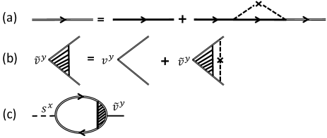
The unavoidable presence of disorder induces a broadening of the quasiparticle states, and vertex corrections that are captured by the diagrams shown in Fig. 2.
In TIs charge impurities appear to be the dominant source of disorder Kim et al. (2012) and so it is expected that they will also be in TI-graphene heterostructures. We therefore model the disorder as a random potential created by an effective 2D distribution of uncorrelated charge impurities with zero net charge placed at an effective distance below the TI’s surface. Direct imaging experiments Beidenkopf et al. (2011) suggest nm, consistent with transport results Kim et al. (2012); Li et al. (2012).
In momentum space, the bare potential created on the TI’s surface by a single charge impurity is where is the average dielectric constant with Culcer et al. (2010); Butch et al. (2010); Beidenkopf et al. (2011); Kim et al. (2012); Li et al. (2012) the dielectric constant for the TI and the dielectric constant of vacuum not (b). The screened disorder potential is where is the dielectric function Hwang et al. (2007); Das Sarma et al. (2011); Triola and Rossi (2012). To obtain the current-driven SOT in the dc limit, and for temperatures much lower than the Fermi temperature , to very good approximation we can assume , where and is the density of states at the Fermi energy.
The lifetime of a quasiparticle in band with momentum is given by
| (2) |
where is the impurity density and is the Bloch state with momentum and band index . In the remainder, we set . Kim et al. (2012) The transport time , that renormalizes the expectation value of the velocity operator, is obtained by introducing the factor under the sum on the right hand side of Eq. (2), and in general differs from the lifetime Das Sarma and Stern (1985); Nomura and MacDonald (2007); Rossi and Das Sarma (2008); Rossi et al. (2009); Lu et al. (2016).
For a charge current in the direction the non equilibrium spin density is polarized in the direction. Due to the rotational symmetry of the system we have and . Without loss of generality we can assume the current to be in the direction. Within the linear response regime, taking into account the presence of disorder, the response function of the system can be obtained by calculating the diagrams shown in Fig. (2). The diagram in Fig. (2a) represents the equation for the self-energy in the first Born approximation, where the double line represents the disorder-dressed electrons’ Green’s function, the single line the electron’s Green’s function for the clean system, and the dashed lines scattering events off the impurities. The diagram in Fig. (2b) corresponds to the equation for the renormalized velocity vertex, , at the ladder level approximation. In the long wavelength, dc, limit we have
| (3) |
where is the expectation value of the i-th component of the spin density operator, with the expectation value of the i-th component of the velocity operator , and are the retarded and advanced Green’s functions, respectively, for electrons with momentum and band index .
III Results
In this section, we present our results for the transport properties and current-induced spin density accumulation of TI-graphene heterostructures.
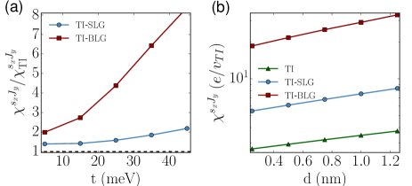
We define the average , as . Figs. 3 (a), (b) show , and , respectively, for a TI’s surface, a TI-SLG heterostructure, and a TI-BLG heterostructure, with meV. We see that the presence of a graphene layer strongly increases both , and , and that such increase is dramatic for the case when the layer is BLG. , and are larger in BLG-TI than TI-SLG because, especially at low energies, BLG has a larger density of states than SLG causing , that enters in the denominator in Eq. (2), and therefore , and to be larger in BLG than in SLG. Notice that , increase after adding a graphene layer even in the limit when as shown by the dashed lines in Fig. 3. This is due to the fact that the graphene layer screens the dominant source of disorder in the TI even when . Changes in have only minor quantitative effects as long as .
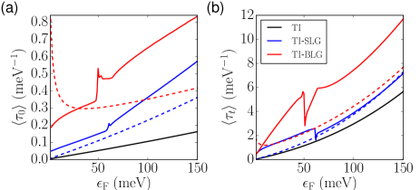
Figure 4 (a) shows the dependence of on for TI, TI-SLG, and TI-BLG for meV, and meV with out-of-plane magnetization (solid lines). The dashed lines corresponds to the case . The inset shows a sketch of the system, with charge flowing in the -direction. The direction of the spin accumultion on the top and bottom layer is indicated by the arrows on the electrons. The insertion of a graphene layer strongly enhances the current-induced spin density response and therefore the SOT. Now, we consider in-plane magnetization. In this case, the Fermi surface is not isotropic as for out-of-plane magnetization, which makes the computation of scattering time, transport times, and the Edelstein effect more challenging. For concreteness, we assume the magnetization direction to be (). Fig. 4 (b) shows as a function of for in-plane () magnetization and meV, dashed lines. The red lines correspond to a TI-BLG-FM and the black lines to a TI-FM heterostructure. We obtained an enhancement as large as the one obtained for out-of-plane magnetization (), solid lines.
We find that changes in have a strong impact on . Figure 4 (c) shows that by increasing the enhancement of the SOT can be raised to values as high as 100 in TI-BLG heterostructures due to the flattening and consequent increase of the DOS of the TI-like bands (see Appendix A).
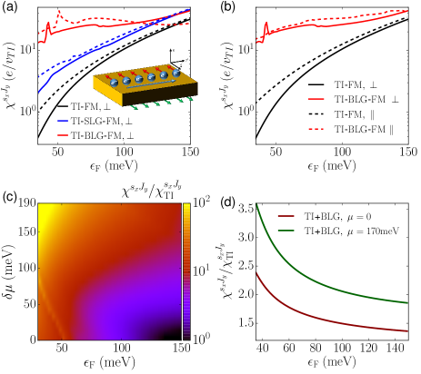
The results of Fig. 4 show that in TI-SLG and TI-BLG heterostructures the current-induced SOT can be expected to be much higher than in TI surfaces alone. They show that for TI-BLG systems there is a large range of values of , for which the enhancement of due to the presence of the BLG is consistently close to 10 or larger, Fig. 4 (c).
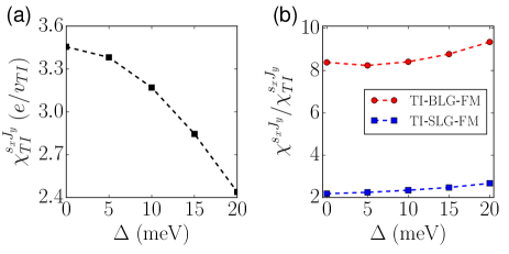
We also find that the strong enhancement of is not affected significantly by the value of , as shown in Fig. (5), where we plot as a function of at meV. In Fig. (5) (a) we plot for TI-FM, while (5) (b) shows the response function for TI-SLG(BLG)-FM normalized to the response in a TI-FM system.
In addition, in a TI-graphene heterostructure, by placing the source and drain on the graphene (BLG) and taking into account the high mobility of graphene (BLG), it is possible to force most of the current to flow within graphene (BLG) and the TI’s surface adjacent to it. Therefore, we can minimize the amount of spin density accumulation with opposite polarization that a current flowing in the TI’s bottom surface generates. This fact should further increase the net SOT.
The large enhancement of the spin density accumulation in TI-graphene systems is due to two main reasons: (i) the survival, after hybridization, of TI-like bands well separated from Rashba bands; (ii) the strong enhancement of the relaxation time and transport time due to the additional screening by the graphene layer of the dominant source of disorder. It is important to notice that the presence of the Rashba bands, see Fig. 1, not only is not essential for the enhancement of the spin density accumulation but it can be detrimental given that the Rashba bands give a with opposite sign of the TI-like bands. This fact can be seen at large Fermi energies for BLG-TI in Fig. 4 (a): for meV the Fermi surface intersect the Rashba bands that by giving a contribution to opposite to the TI-like bands brings the net SOT of TI-BLG to be slightly lower than the SOT of TI-alone. Point (ii) explains the fact the , at low energies, is always larger in TI-BLG rather than TI-SLG given that and are larger in TI-BLG than in TI-SLG. In addition, it explains the fact that even in the limit when there is no hybridization between the TI and the graphene bands, i.e. t=0 due for example to a large twist angle (see Appendix B), the spin-current correlation function in TI-graphene systems is still larger than in TIs alone for the experimentally relevant case where charge impurities are the dominant source of disorder, as shown in Fig. 4 (d).
In Fig. 6 (a), we show the current-induced spin density accumulation response function dependence on the tunneling amplitude , normalized to the TI response. As is increased, TI and graphene hybridize more strongly, leading to a larger SOT. However, even at vanishing tunneling, an enhancement is still present.
In Fig. 6 (b), we plot as a function of the effective distance from the TI surface to the effective layer of impurities . The further away the impurities are located, the weaker the disorder, and therefore the larger the expected SOT.
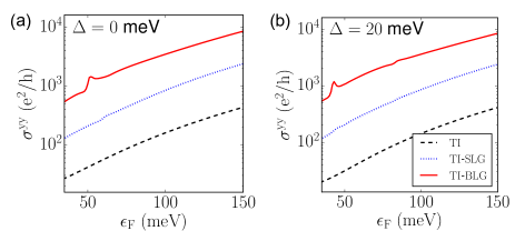
To estimate the efficiency of the current-induced SOT in TI-graphene heterostructures, we calculate the associated dc longitudinal conductivity for the same parameters. In the linear-response, long-wavelength, regime we have
| (4) |
Fig. 7 (a) shows for TI, TI-SLG, and TI-BLG as a function of in the limit . We see that the presence of a graphene layer enhances the conductivity of the system by an order of magnitude or more. Fig. 7 (b) shows that the exchange term does not affect significantly. The results shown in Fig. 7 (b) imply that in TI-graphene heterostroctures not only the current-induced SOT can be much larger than in TIs alone, but also that the generation of the SOT is much less dissipative. For example, for an applied electric fields of the order of 0.1 m, we can reach a conservative spin density accumulation . For typical carrier density in graphene (), we have .
IV Conclusions
In conclusion, we have shown that in magnetic TI-graphene heterostructures the non-equilibrium uniform spin density accumulation induced by a charge current can be 10-100 times higher than in TIs alone giving rise to a giant Edelstein effect. The reasons for these enhancements are (i) the additional screening by the graphene layer of the dominant source of disorder; (ii) the fact that graphene and the TI’s surface are almost commensurate making possible a strong hybridization of the TI’s and graphene’s states; (iii) the fact that the spin structure of the hybridized bands has a spin structure very similar to the one of the original TI’s band for a large range of dopings; (iv) the fact that graphene is the ultimate 2D system, only one-atom thick. These facts and our results suggest the TI-graphene systems are very good candidates to realize all-electric efficient magnetization switching.
ACKNOWLEDGEMENTS
We acknowledge helpful discussions with Yong Chen and Saroj Dash. MRV and ER acknowledge support from NSF Grant No. DMR-1455233 and ONR Grant No. N00014-16-1-3158. ER also acknowledges support from ARO Grant No W911NF-16-1-0387, and the United States-Israel Binational Science Foundation, Jerusalem, Israel. In addition, MRV and ER thank the hospitality of the Spin Phenomena Interdisciplinary Center (SPICE), where this project was initiated. JS and GS acknowledge the support by Alexander von Humboldt Foundation, the ERC Synergy Grant SC2 (No. 610115), and the Transregional Collaborative Research Center (SFB/TRR) 173 SPIN+X.
Appendix A TI-BLG BAND STRUCTURE
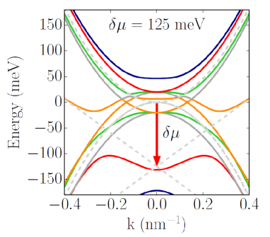
As long as the interlayer tunneling between the carbon atoms in bilayer graphene is much larger than the expected tunneling between the TI’s surface and the graphenic layer any difference between the tunneling strength between the carbon layers forming BLG and the TI will give very negligible effects. Considering that in bilayer graphene the interlayer tunneling is 350 meV, and the fact that for the TI-graphene tunneling we only consider values smaller than 45 meV for all our results is . In this limit, at low energies ( meV), BLG can be treated as 2D system with the effective Hamiltonian presented in the main text.
Fig. 1 (e) in the main text shows the bands of a TI-BLG systems
for which the exchange field meV and .
Fig 3 shows that the strongest enhancement of the SOT happens
for TI-BLG systems when . It is therefore
interesting to see how the low-energy bands of TI-BLG
are affected by a nonzero value of .
Fig. 8 shows the band structure of TI-BLG
for the case when meV in the absence of any exchange field.
We see that one of TI-like bands (shown in orange) becomes much flatter:
the high density of states of this band explains the high values of SOT
for TI-graphene systems when .
Appendix B INVERSE SPIN GALVANIC EFFECT IN TWISTED TI-GRAPHENE HETEROSTRUCTURES
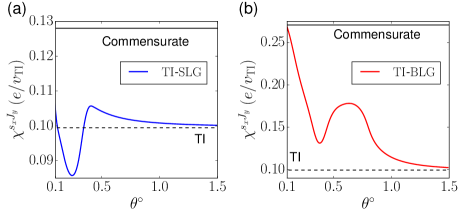
It can expected that even when the stacking of the graphenic layer and the TI’s surface is incommensurate, the screening of the charge impurities by the graphenic layer will lead to a strong enhancement of and and therefore of the SOT. The accurate treatment of the realistic case in which the main source of disorder are charge impurities for incommensurate stackings requires the calculation of the dielectric constant for incommensurate structures, a task that is beyond the scope of the present work. For this reason, to exemplify how the presence of a small twist angle between the graphenic layer and the TI surface, giving rise to an incommensurate stacking, affects the calculation of the SOT, we consider a very simple model for the effect of the disorder: we simply assume that the disorder gives rise to a constant quasiparticle broadening.
Let , where is the magnitude of the graphene point. The dimensionless parameter , where , measures the strength of the coupling between the graphenic layer and the TI. For we can obtain the electronic structure using the weak coupling theory for twisted systems Lopes dos Santos et al. (2007); Bistritzer and MacDonald (2011); Mele (2012) that for the case of a TI-graphene heterostructures we presented in Ref. Zhang et al. (2014). After obtaining the electronic structure in the regime , we can obtain . To understand how the response between the commensurate and the incommensurate regimes differ, we have calculated assuming a constant quasiparticle broadening meV, with meV, , and meV for a range of values of for which the weak coupling theory is valid. The dependence of , per valley, as a function of for TI-SLG and TI-BLG is shown in Fig. 9. As to be expected, the results show that in the incommensurate case the response is smaller than in the commensurate case. However, they also show, in particular for the case in which the graphenic layer is BLG, that a TI-graphene heterostructure is expected to have stronger , and therefore a stronger inverse spin-galvanic effect, even in the incommensurate regime and for the case in which the disorder is modeled very simply.
References
- Žutić et al. (2004) I. Žutić, J. Fabian, and S. Das Sarma, Rev. Mod. Phys. 76, 323 (2004).
- Sinova et al. (2015) J. Sinova, S. O. Valenzuela, J. Wunderlich, C. H. Back, and T. Jungwirth, Rev. Mod. Phys. 87, 1213 (2015).
- Hasan and Kane (2010) M. Z. Hasan and C. L. Kane, Rev. Mod. Phys. 82, 3045 (2010).
- Qi and Zhang (2011) X.-L. Qi and S.-C. Zhang, Rev. Mod. Phys. 83, 1057 (2011).
- Sinova and Žutić (2012) J. Sinova and I. Žutić, Nature Materials 11, 368 (2012).
- Brataas et al. (2012) A. Brataas, A. D. Kent, and H. Ohno, Nature Materials 11, 372 (2012).
- Jungwirth et al. (2012) T. Jungwirth, J. Wunderlich, and K. Olejník, Nature Materials 11, 382 (2012).
- Bauer et al. (2012) G. E. W. Bauer, E. Saitoh, and B. J. van Wees, Nature Materials 11, 391 (2012).
- Dyakonov and Perel (1971) M. Dyakonov and V. Perel, Physics Letters A 35, 459 (1971).
- Edelstein (1990) V. Edelstein, Solid State Communications 73, 233 (1990).
- Dyakonov (Ed.) M. I. Dyakonov (Ed.), Spin physics in semiconductors, Springer Series in Solid-State Sciences, Vol. 157 (Springer, New York, 2008).
- Kurebayashi et al. (2014) H. Kurebayashi, J. Sinova, D. Fang, A. C. Irvine, T. D. Skinner, J. Wunderlich, V. Novák, R. P. Campion, B. L. Gallagher, E. K. Vehstedt, L. P. Zârbo, K. Výborný, A. J. Ferguson, and T. Jungwirth, Nature Nanotechnology 9, 211 (2014).
- Garate and Franz (2010) I. Garate and M. Franz, Phys. Rev. Lett. 104, 146802 (2010).
- Yokoyama et al. (2010) T. Yokoyama, J. Zang, and N. Nagaosa, Phys. Rev. B 81, 241410 (2010).
- Sakai and Kohno (2014) A. Sakai and H. Kohno, Phys. Rev. B 89, 165307 (2014).
- Fischer et al. (2016) M. H. Fischer, A. Vaezi, A. Manchon, and E.-A. Kim, Phys. Rev. B 93, 125303 (2016).
- Ndiaye et al. (2017) P. B. Ndiaye, C. A. Akosa, M. H. Fischer, A. Vaezi, E.-A. Kim, and A. Manchon, Phys. Rev. B 96, 014408 (2017).
- Mellnik et al. (2014) A. R. Mellnik, J. S. Lee, A. Richardella, J. L. Grab, P. J. Mintun, M. H. Fischer, A. Vaezi, A. Manchon, E.-A. Kim, N. Samarth, and D. C. Ralph, Nature 511, 449 (2014).
- Fan et al. (2016) Y. Fan, X. Kou, P. Upadhyaya, Q. Shao, L. Pan, M. Lang, X. Che, J. Tang, M. Montazeri, K. Murata, L.-T. Chang, M. Akyol, G. Yu, T. Nie, K. L. Wong, J. Liu, Y. Wang, Y. Tserkovnyak, and K. L. Wang, Nature Nanotechnology 11, 352 (2016).
- Novoselov et al. (2005) K. S. Novoselov, A. K. Geim, S. V. Morozov, D. Jiang, M. I. Katsnelson, I. V. Grigorieva, S. V. Dubonos, and A. A. Firsov, Nature 438, 197 (2005).
- Zhang et al. (2005) Y. Zhang, Y.-W. Tan, H. L. Stormer, and P. Kim, Nature 438, 201 (2005).
- Castro Neto et al. (2009) A. H. Castro Neto, F. Guinea, N. M. R. Peres, K. S. Novoselov, and A. K. Geim, Rev. Mod. Phys. 81, 109 (2009).
- Das Sarma et al. (2011) S. Das Sarma, S. Adam, E. H. Hwang, and E. Rossi, Rev. Mod. Phys. 83, 407 (2011).
- Lee and Fabian (2016) J. Lee and J. Fabian, Phys. Rev. B 94, 195401 (2016).
- Vaklinova et al. (2016) K. Vaklinova, A. Hoyer, M. Burghard, and K. Kern, Nano Letters 16, 2595 (2016).
- Tian et al. (2016) J. Tian, T.-F. Chung, I. Miotkowski, and Y. P. Chen, (2016), arXiv:1607.02651 .
- not (a) In both experiments the currents are AC and the values provided in the text are the r.m.s. values. In the setup used in Ref. Mellnik et al. (2014) a big fraction of the current flows through the bulk of the TI and the ferromagnetic metal (Py) placed on top of the TI, whereas in the setup used in Ref. Fan et al. (2016), in optimal conditions, most of the current flows through the TI’s surfaces.
- Haigh et al. (2012) S. J. Haigh, A. Gholinia, R. Jalil, S. Romani, L. Britnell, D. C. Elias, K. S. Novoselov, L. A. Ponomarenko, A. K. Geim, and R. Gorbachev, Nature Materials 11, 764 (2012).
- Jin and Jhi (2013) K.-H. Jin and S.-H. Jhi, Phys. Rev. B 87, 075442 (2013).
- Wallbank et al. (2013) J. R. Wallbank, M. Mucha-Kruczyński, and V. I. Fal’ko, Phys. Rev. B 88, 155415 (2013).
- Zhang et al. (2014) J. Zhang, C. Triola, and E. Rossi, Phys. Rev. Lett. 112, 096802 (2014).
- Steinberg et al. (2015) H. Steinberg, L. A. Orona, V. Fatemi, J. D. Sanchez-Yamagishi, K. Watanabe, T. Taniguchi, and P. Jarillo-Herrero, Phys. Rev. B 92, 241409 (2015).
- Bian et al. (2016) G. Bian, T.-F. Chung, C. Chen, C. Liu, T.-R. Chang, T. Wu, I. Belopolski, H. Zheng, S.-Y. Xu, D. S. Sanchez, N. Alidoust, J. Pierce, B. Quilliams, P. P. Barletta, S. Lorcy, J. Avila, G. Chang, H. Lin, H.-T. Jeng, M.-C. Asensio, Y. P. Chen, and M. Z. Hasan, 2D Materials 3, 021009 (2016).
- Ponomarenko et al. (2013) L. A. Ponomarenko, R. V. Gorbachev, G. L. Yu, D. C. Elias, R. Jalil, A. A. Patel, A. Mishchenko, A. S. Mayorov, C. R. Woods, J. R. Wallbank, M. Mucha-Kruczynski, B. A. Piot, M. Potemski, I. V. Grigorieva, K. S. Novoselov, F. Guinea, V. I. Fal’Ko, and A. K. Geim, Nature 497, 594 (2013).
- Spataru and Léonard (2014) C. D. Spataru and F. Léonard, Phys. Rev. B 90, 085115 (2014).
- Lee et al. (2015) P. Lee, K.-H. Jin, S. J. Sung, J. G. Kim, M.-T. Ryu, H.-M. Park, S.-H. Jhi, N. Kim, Y. Kim, S. U. Yu, K. S. Kim, D. Y. Noh, and J. Chung, ACS Nano 9, 10861 (2015).
- Rajput et al. (2016) S. Rajput, Y.-Y. Li, M. Weinert, and L. Li, ACS Nano 10, 8450 (2016).
- Ren et al. (2010) Z. Ren, A. A. Taskin, S. Sasaki, K. Segawa, and Y. Ando, Phys. Rev. B 82, 241306 (2010).
- Xiong et al. (2012) J. Xiong, A. C. Petersen, D. X. Qu, Y. S. Hor, R. J. Cava, and N. P. Ong, Physica E 44, 917 (2012).
- Arakane et al. (2012) T. Arakane, T. Sato, S. Souma, K. Kosaka, K. Nakayama, M. Komatsu, T. Takahashi, Z. Ren, K. Segawa, and Y. Ando, Nature Comm. 3, 636 (2012).
- Xia et al. (2013) B. Xia, P. Ren, A. Sulaev, P. Liu, S. Q. Shen, and L. Wang, Phys. Rev. B 87, 085442 (2013).
- Segawa et al. (2012) K. Segawa, Z. Ren, S. Sasaki, T. Tsuda, S. Kuwabata, and Y. Ando, Phys. Rev. B 86, 075306 (2012).
- Xu et al. (2014) Y. Xu, I. Miotkowski, C. Liu, J. Tian, H. Nam, N. Alidoust, J. Hu, C.-K. Shih, M. Z. Hasan, and Y. P. Chen, Nature Physics 10, 956 (2014).
- Durand et al. (2016) C. Durand, X.-G. Zhang, S. M. Hus, C. Ma, M. A. McGuire, Y. Xu, H. Cao, I. Miotkowski, Y. P. Chen, and A.-P. Li, Nano Letters 16, 2213 (2016).
- Xu et al. (2016) Y. Xu, I. Miotkowski, and Y. P. Chen, Nat Commun 7 11434 (2016).
- Lee et al. (2016) C. Lee, F. Katmis, P. Jarillo-Herrero, J. S. Moodera, and N. Gedik, Nature Communications 7, 12014 (2016).
- Katmis et al. (2016) F. Katmis, V. Lauter, F. S. Nogueira, B. A. Assaf, M. E. Jamer, P. Wei, B. Satpati, J. W. Freeland, I. Eremin, D. Heiman, P. Jarillo-Herrero, and J. S. Moodera, Nature 533, 513 (2016).
- Yang et al. (2014) W. Yang, S. Yang, Q. Zhang, Y. Xu, S. Shen, J. Liao, J. Teng, C. Nan, L. Gu, Y. Sun, K. Wu, and Y. Li, Applied Physics Letters 105, 092411 (2014).
- Sinitsyn et al. (2007) N. A. Sinitsyn, A. H. MacDonald, T. Jungwirth, V. K. Dugaev, and J. Sinova, Phys. Rev. B 75, 045315 (2007).
- Kim et al. (2012) D. Kim, S. Cho, N. P. Butch, P. Syers, K. Kirshenbaum, S. Adam, J. Paglione, and M. S. Fuhrer, Nature Physics 8, 459-463 (2012).
- Beidenkopf et al. (2011) H. Beidenkopf, P. Roushan, J. Seo, L. Gorman, I. Drozdov, Y. S. Hor, R. J. Cava, and A. Yazdani, Nature Physics 7, 939-943 (2011).
- Li et al. (2012) Q. Li, E. Rossi, and S. Das Sarma, Phys. Rev. B 86, 235443 (2012).
- Culcer et al. (2010) D. Culcer, E. H. Hwang, T. D. Stanescu, and S. Das Sarma, Phys. Rev. B 82, 155457 (2010).
- Butch et al. (2010) N. P. Butch, K. Kirshenbaum, P. Syers, A. B. Sushkov, G. S. Jenkins, H. D. Drew, and J. Paglione, Phys. Rev. B 81, 241301 (2010).
- not (b) Strictly speaking the value is only valid for the case of a magnetically doped TI. However, given the large static dielectric constant of the TI, the error made by approximating the FM’s dielectric constant by the vacuum’s is negligible. For EuS, the suggested insulating FM, giving an effective average dielectric constant , instead of the used .
- Hwang et al. (2007) E. H. Hwang, S. Adam, and S. Das Sarma, Phys. Rev. Lett. 98, 186806 (2007).
- Triola and Rossi (2012) C. Triola and E. Rossi, Phys. Rev. B 86, 161408 (2012).
- Das Sarma and Stern (1985) S. Das Sarma and F. Stern, Phys. Rev. B 32, 8442 (1985).
- Nomura and MacDonald (2007) K. Nomura and A. H. MacDonald, Phys. Rev. Lett. 98, 076602 (2007).
- Rossi and Das Sarma (2008) E. Rossi and S. Das Sarma, Phys. Rev. Lett. 101, 166803 (2008).
- Rossi et al. (2009) E. Rossi, S. Adam, and S. D. Sarma, Phys. Rev. B 79, 245423 (2009).
- Lu et al. (2016) C.-P. Lu, M. Rodriguez-Vega, G. Li, A. Luican-Mayer, K. Watanabe, T. Taniguchi, E. Rossi, and E. Y. Andrei, PNAS 113, 6623 (2016).
- Lopes dos Santos et al. (2007) J. Lopes dos Santos, N. Peres, and A. Castro Neto, Phys. Rev. Lett. 99, 256802 (2007).
- Bistritzer and MacDonald (2011) R. Bistritzer and A. H. MacDonald, Proc. National Acad. Sciences United States Am. 108, 12233 (2011).
- Mele (2012) E. J. Mele, Journal of Physics D Applied Physics 45, 154004 (2012).