Intrinsic Electron Mobility Limits in -Ga2O3
Abstract
By systematically comparing experimental and theoretical transport properties, we identify the polar optical phonon scattering as the dominant mechanism limiting electron mobility in Ga2O3 to 200 cmVs at 300 K for donor doping densities lower than 1018 cm-3. In spite of similar electron effective mass of Ga2O3 to GaN, the electron mobility is 10 lower because of a massive Frhlich interaction, due to the low phonon energies stemming from the crystal structure and strong bond ionicity. Based on the theoretical and experimental analysis, we provide an empirical expression for electron mobility in Ga2O3 that should help calibrate its potential in high performance device design and applications.
Ga2O3 has recently emerged as an ultra wide-bandgap semiconductor eVPR65 ; APL2010 with 300 K electron mobility 150 cmVs,APEX15 attractive enough to potentially offer high-voltage electronic device performanceSST2016 that is beyond the reach of the currently successful GaN and SiC platforms. With the recent success in the synthesis of large-area bulk single crystal substrates and availability of nanomembranes,SST2016 ; JCG2013 ; APL14 Ga2O3 becomes a transparent conductive oxide (TCO) with significant potential. It advances the field of oxide electronics from the traditional IGZO, perovskites (SrTiO3, BaSnO3, etc), and ZnO.AM2012 ; Nature2004 ; APL2003 In this work, we have explored the physics of the intrinsic electron mobility limits in this material system and obtained expressions that should prove useful in device design.
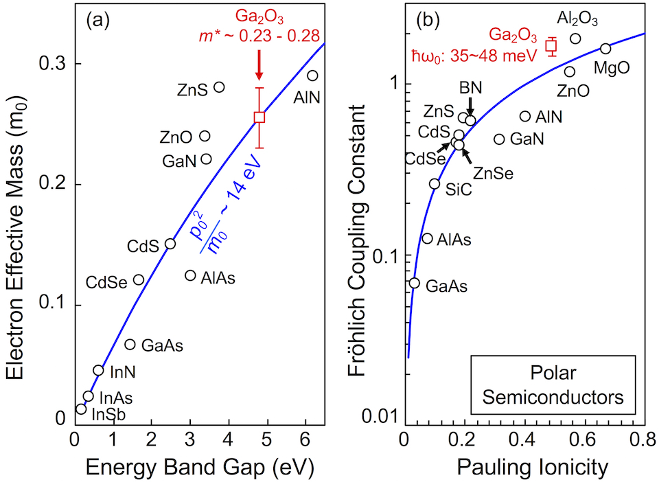
Since the Drude electron mobility is determined by the conduction band minimum (CBM) effective mass , electron charge , and the low-field scattering rate , we investigate term first. From standard theory, of sp3-bonded direct gap semiconductors with the CBM at the point is related to by PRB77 , where is the de-Broglie momentum of electrons at the Brillouin-zone edge with the electron wavevector, the lattice constant, the Planck’s constant, and the free electron rest mass. Figure 1 (a) shows for various compound semiconductors as a function of .PRB01 ; Adachi05 The solid blue line shows the prediction with 14 eV. Variations in lattice constant, Land factor, slight indirectness of the bandgap, and the ionicity of the semiconductor can explain the slight deviations,PRB77 but the overall fit and the trend it predicts overrides these details – with a large 4.6 - 4.9 eV,PR65 ; APL2010 Ga2O3 boasts a relatively low ,SSC04 ; APL2010 as indicated in Fig. 1 (a). Unlike several other complex oxides and perovskites, where or orbital conduction bands lead to heavy , Ga2O3 has a small because the CBM electron states derive from the hybridization of the Ga orbitals. Now because of Ga2O3 is similar to that of GaN, one may initially expect the 300 K Drude mobility to be similar to bulk GaN (1500 cmVs). However, the maximum experimentally measured 300 K electron mobility in bulk single-crystal Ga2O3 with little or no dislocations is 110-150 cm2/Vs,APL08 ; CRT10 ; JAP11 ; APEX15 ; APL14 nearly an order of magnitude lower than GaN. Potential electronic device applications of Ga2O3 beg the question whether the reported lower mobilities are intrinsic, or can be improved by eliminating extrinsic defects. Answering this question is the subject of this work.
We turn to the scattering rate to explain the difference in mobility between GaN and Ga2O3. Because the Ga-O bond is strongly ionic,APL06 one can expect polar optical (PO) phonons to play an important role in limiting the room-temperature electron mobility, similar to GaN and GaAs.PRB2000 ; PRB86 The PO phonon energy intersects the electron bandstructure at the characteristic wavevector , which defines a characteristic Born-effective fieldSeeger , where is the vacuum permittivity, and and are the low- and high-frequency relative dielectric constant of the semiconductor. For polar semiconductors, the strength of electron-PO phonon (e-PO) interaction is dictated by the dimensionless Frhlich coupling constant:AP54
| (1) |
Figure. 1 (b) shows for several polar semiconductors plotted against their Pauling ionicity: Pauling , where is the difference of the electronegativity of the two elements in the bond. The blue solid trend line shows the empirical relation , showing that increases with , i.e., strongly ionic bonds lead to stronger e-PO interaction. Recent polarized reflectance measurements performed by Onuma et al.APL16 show that the lowest optical phonon modes in Ga2O3 are in the range of 35-48 meV, which leads to 0.21, as shown by the red open square in Fig. 1 (b). This indicates a massive Frhlich coupling, nearly 3 stronger than GaN. Polaron effects, such as self-trapped holes due to their heavy band,PR69 can be expected to be strong in Ga2O3, renormalizing the electron effective mass ,Seeger which is used in the following transport properties study.
For non-degenerate dilute carrier densities at high temperatures () when , where is the Boltzmann constant, the PO phonon scattering limited electron mobilityJAP1995 . From the 300 K 1500 cm2/Vs of bulk GaN, one can estimate in -Ga2O3 to be 88-141 cm2/Vs. This value agrees with the reported 110-150 cm2/Vs in -Ga2O3 at 300 K.APL08 ; CRT10 ; JAP11 ; APEX15 ; APL14 This simple analysis indicates that PO phonon is likely the dominant room-temperature scattering mechanism in -Ga2O3 and rules out other possibilities of intrinsic scattering mechanisms.
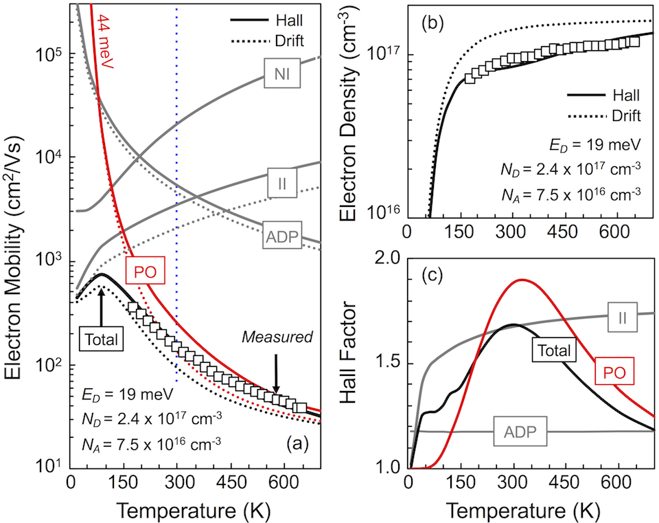
Hall-effect measurements were performed over a wide temperature range from 180 K to 650 K using a Lakeshore Hall system on unintentionally-doped Ga2O3 bulk substrates from Tamura Corporation. These substrates were diced into 5 mm5 mm square pieces. Ti/Pt Ohmic contacts were deposited on the four corners of the sample in Van de Pauw geometry followed by rapid thermal annealing (2 min, 480 ∘C, Nitrogen atmosphere). Figure 2 (a) shows the measured temperature-dependent electron mobilities in Ga2O3, and Figure 2 (b) shows the measured electron density, both as open squares. The lines in Figure 2 (a) show the calculated mobility resolved into the individual scattering mechanisms by ADP (), ionized () and neutral impurity () scattering, and the red line shows the polar-optical scattering limited mobility . These calculations are described after a brief discussion. The solid line in Figure 2 (b) is the calculated Hall-effect carrier density based on the Hall mobility and the dashed line is , corresponding to the drift mobility .
Figure 2 (c) shows the calculated Hall-factor due to each scattering mechanism and the net with all scattering mechanisms considered, highlighting the difference between and . , , and the ionization energy are from fitting of the temperature-dependent using the neutrality condition: . For the current sample, cm-3, cm-3, and meV. Figure 2 (a) indicates that extrinsic scattering from ionized and neutral impurity dominate the electron mobility at low temperatures up to 150 K. Among intrinsic scattering mechanisms, is higher than the measured mobility by more than one order of magnitude over the entire temperature range. Consequently the only mechanism that limits the electron mobility at high temperatures is PO phonon scattering. The optical phonon energy that explains the measured temperature-dependent is 44 meV, which is very close to the lowest phonon energies from optical spectroscopy measurements reported by Onuma et al.APL16 It lends credence to our claim of the dominance of PO phonon scattering in Ga2O3.
In a recent work, Parisini and Fornari suggested that intrinsic electron mobility in Ga2O3 is controlled by optical deformation potential (ODP) scattering.SST16 It is known that ODP scattering plays an important role in non-polar crystals such as silicon and germanium, and disappears due to symmetry when the CBM is at the point and there are only two atoms in the primitive unit cell.Ridley ; PR48 ; PR56 Ga2O3, with CBM at the point, however has a monoclinic structure with ten atoms in the primitive unit cell, which leads to 30 phonon modes.SSC04 Recent DFT calculation indicates that in -Ga2O3, ODP scattering of electrons at low electric field are negligible compared to the PO phonon scattering,Buffalo16 similar to other polar semiconductors such as GaN and GaAs.PRB2000 ; PRB86 Thus, we do not consider ODP further in this work.
To quantify the dominant role of e-PO scattering in -Ga2O3, the lines of Fig 2 were calculated using the relaxation-time approximation (RTA) solution of the Boltzmann transport equation (BTE). Four scattering mechanisms are considered: ionized impurity (II), neutral impurity (NI), PO phonon, and acoustic deformation potential (ADP). The material parameters used in the calculation are listed in Table 1.
| Parameter | Symbol | Value |
|---|---|---|
| Mass Density (g/cm3) | 5.88111Ref. SST16, . | |
| Sound Velocity (cm/s) | 6.8105222Ref. APL15, ; ADP, . | |
| Acoustic Deformation Potential (eV) | 6.9 222Ref. APL15, ; ADP, . | |
| Static Dielectric Constant | 10.2 333Ref. APL94, ; JAP95, ; APL02, . | |
| High-frequency Dielectric Constant | 3.57333Ref. APL94, ; JAP95, ; APL02, . | |
| CBM Electron Effective Mass (m0) | 0.28444Ref. APL2010, . | |
| PO Phonon Energy (meV) | 44 (fitted) |
The RTA solution of BTE gives the average electron drift mobility for carriers moving in 3-dimensions:Chihiro
| (2) |
where is the electron energy, is the Fermi-Dirac distribution, and is the momentum relaxation time. The Hall factor is calculated to obtain the Hall mobility and the Hall electron density , where is the mobile electron density. due to each individual scattering mechanism is evaluated using Fermi’s golden rule. Phonon and neutral impurity scattering are assumed to be unscreened, while ionized impurity scattering is statically screened by free carriers with the reciprocal Debye screening length: , where is the effective screening carrier density:Wolfe , where and are the densities of donors and compensated acceptors. is the Fermi integral, , is the Fermi level, and the CBM energy. of ionized impurity scattering is given by Brooks-Herring model:BrooksHerring , where , . The scattering rate due to neutral impurities is given by:PR50 , where . For ADP scattering: , parameters here are defined in Table 1. due to PO phonon scattering is
| (3) | |||||
where , and is the equilibrium phonon number. The and subscripts are for PO phonon emission and absorption. The net momentum relaxation rate is obtained using Matthiessen’s rule: .
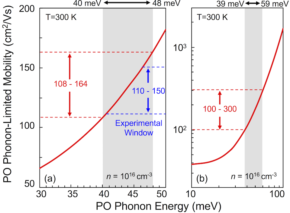

Figure 3 shows the the sensitivity of (drift) to the value of used in Eq. 3 at 300 K. When varies from 40 meV to 48 meV ( meV), varies from 108 164 cm2/Vs. These values fully cover the reported experimental electron mobility values from various groups and are within acceptable experimental errors. Even if we relax the range to 100 300 cm2/Vs (Fig. 3 (b)), where the 300 cm2/Vs value is the qualitatively estimated intrinsic mobility predicted by Sasaki et al.,APEX12 the corresponding ranges from 39 to 59 meV. Therefore in -Ga2O3 that limits electron transport at room temperature is inferred to be not far from 44 meV as we have extracted from our experimental results. With the e-PO interaction established as the dominant intrinsic scattering mechanism, it is important to study the relative importance of impurity scattering on electron mobility. Figure 4 (a) and (b) show the calculated as a function of at 77 K and 300 K. For 77 K, the solid and dashed lines show mobilities with and cm-3. As seen in Fig. 4 (a), intrinsic electron mobility higher than 10,000 cm2/Vs can be achieved in very clean samples with 1015 cm-3. However, introducing severely decreases electron mobilities through ionized impurity scattering. When = cm-3 and cm-3, the mobility is reduced to 350 cm2/Vs. This explains the experimentally observed low-temperature low electron mobilities,JAP11 ; APEX15 and also much higher mobilitiesKumagai ( 7,000 cm2/Vs) in cleaner samples. In Fig. 4 (b), the black line shows the net with all four scattering mechanisms considered, the red solid line indicates with = 44 meV and the blue solid line show mobility limited by ionized and neutral impurity scattering. The open symbols are experimental results from various groups. Figure 4 (c) shows as a function of temperature for various . The arrows denote the density of neutral impurities. The heavier the doping, the more unionized impurities are introduced. Therefore both ionized and neutral impurity scattering become increasingly important in determining electron mobilities as temperature decreases and as the doping concentration increases.
To estimate around or higher than 300 K, we derived the following expressions:
| (4) |
| (5) |
| (6) |
where , and are the Hall factors of PO phonon scattering and ionized impurity scattering, respectively. At 300 K, the empirical expressions and are used to describe the doping dependence of Hall factors. The first and second terms in the brackets of Eq. 4 correspond to the PO phonon absorption and emission, respectively.
The dashed lines in Fig. 4 (b) show the net calculated using Eq. 4-6. At 300 K, PO phonon scattering dominates the mobility for lower than a critical doping density determined by the crossover condition . When , neutral impurity introduced by heavy doping severely degrades the electron mobility. For 300 K, 250 cm2/Vs and cm-3. For power devices that typically operate at high temperatures, is captured by the empirical expression:
| (7) |
The 300 K electron mobility calculated using Eq. 7 is shown by blue dots in Fig. 4 (b). This expression, which is valid for 300 K500 K, offers a useful guideline for experiments and is easily embedded in device modeling.
In summary, we studied the intrinsic electron mobility limits in n-doped Ga2O3. We find an extremely strong Frhlich interaction in the material, fueled by the high ionicity of the chemical bonds, and the low optical phonon energies. A PO phonon energy of 44 meV was deduced from the transport properties. The measured room-temperature electron mobility is dominated by PO phonon scattering for low doping densities, and thus has approached the intrinsic mobility limits. Though it is difficult to change the PO phonon energy, one could investigate strain as a potential tool.APL2015 Moreover, similar to III-V semiconductors, the formation of a two-dimensional electron gas (2DEG) at (AlGa)2OGa2O3 heterojunctions is possible with modulation doping. The electron mobility in such a 2DEG is expected to be higher than the bulk due to the relaxation of the momentum conservation in the direction perpendicular to the interface during the electron-PO phonon scattering process, the elimination of neutral impurity potential, and the powerful exponential reduction of ionized impurity scattering by remote doping.
Acknowledgements.
This work was supported by NSF DMREF program (Award Number 1534303). The authors thank Guru Khalsa for useful discussions.References
- (1) H. H. Tippins, Phys. Rev. 140, A316 (1965).
- (2) J. B. Varley, J. R. Weber, A. Janotti, and C. G. Van de Walle, Appl. Phys. Lett. 97, 142106 (2010).
- (3) T. Oishi, Y. Koga, K. Harada, and M. Kasu, Appl. Phys. Express 8, 031101 (2015).
- (4) M. Higashiwaki, K. Sasaki, H. Murakami, Y. Kumagai, A. Koukitu, A. Kuramata, T. Masui, and S. Yamakoshi, Semicond. Sci. Technol. 31, 034001 (2016).
- (5) K. Sasaki, M. Higashiwaki, A. Kuramata, T. Masui, and S. Yamakoshi, J. Crystal Growth 378, 591 (2013).
- (6) W. S. Hwang, A. Verma, H. Peelaers, V. Protasenko, S. Rouvimov, H. G. Xing, A. Seabaugh, W. Haensch, C. Van de Walle, Z. Galazka, et al., Appl. Phys. Lett. 104, 203111(2014).
- (7) E. Fortunato, P. Barquinha, and R. Martins, Adv. Mater. 24, 2945 (2012).
- (8) A. Ohtomo and H. Y. Hwang, Nature 427, 423 (2004).
- (9) R. L. Hoffman, B. J. Norris, and J. F. Wager, Appl. Phys. Lett. 82, 733 (2003).
- (10) C. Hermann and C. Weisbuch, Phys. Rev. B 15, 823 (1977).
- (11) J. T. Devreese, V. M. Fomin, E. P. Pokatilov, E. A. Kotomin, R. Eglitis, and Y. F. Zhukovskii, Phys. Rev. B. 63, 184304 (2001).
- (12) S. Adachi, Properties of Group-IV, III-V and II-VI Semiconductors (Wiley, Chichester, 2005).
- (13) K. Yamaguchi, Solid State Commun. 131, 739 (2004).
- (14) E. G. Vllora, K. Shimamura, T. Ujiie, and K. Aoki, Appl. Phys. Lett. 92, 202118 (2008).
- (15) Z. Galazka, R. Uecker, K. Irmscher, M. Albrecht, D. Klimm, M. Pietsch, M. Brtzam, R. Bertram, S. Ganschow, and R. Fornari, Cryst. Res. Technol. 45, 1229 (2010).
- (16) K. Irmscher, Z. Galazka, M. Pietsch, R. Uecker, and R. Fornari, J. Appl. Phys. 110, 063720 (2011).
- (17) H. He, M. A. Blanco, and R. Pandey, Appl. Phys. Lett. 88, 261904 (2006).
- (18) B. K. Ridley, B. E. Foutz, and L. F. Eastman, Phys. Rev. B 61, 16862 (2000).
- (19) K. Hirakawa and H. Sakaki, Phys. Rev. B 33, 8291 (1986).
- (20) K. Seeger, Semiconductor Physics (9th Edition, Springer, New York, 2004).
- (21) H. Frhlich, Advances in Physics 3, 325 (1954).
- (22) L. Pauling, The Nature of the Chemical Bond (3rd Edition, Cornell University Press)
- (23) T. Onuma, S. Saito, K. Sasaki, K. Goto, T. Masui, T. Yamaguchi, T. Honda, A. Kuramata, and M. Higashiwaki, Appl. Phys. Lett. 108, 101904 (2016).
- (24) A. Norman Jette, T. L. Gilbert, and T. P. Das, Phys. Rev. 184, 884 (1969).
- (25) B. L. Gelmont, M. Shur, and M. Stroscio, J. Appl. Phys. 77, 657 (1995).
- (26) A. Parisini and R. Fornari, Semicond. Sci. Technol. 31, 035023 (2016).
- (27) B. K. Ridley, Quantum Processed in Semiconductors (4th Edition, Clarendon Press, Oxford, 1999).
- (28) R. Seitz, Phys. Rev. 73, 549 (1948).
- (29) W. A. Harrison, Phys. Rev. 104, 1281 (1956).
- (30) K. Ghosh and U. Singisetti, Appl. Phys. Lett. 109, 072102 (2016).
- (31) Z. Guo, A. Verma, X. F. Wu, F. Y. Sun, A. Hickman, T. Masui, A. Kuramata, M. Higashiwaki, D. Jena, and T. F. Luo, Appl. Phys. Lett. 106, 111909 (2015).
- (32) The deformation potential of a particular band induced by a certain phonon mode through electron-phonon interaction is given by , where is the energy change of band relative to that in the equilibrium structure, is the lattice constant of the equilibrium structure, and is the lattice constant change due to a structural perturbation from phonon mode . The calculation is carried out by first displacing the atomic coordinates in the optimized cell from their equilibrium positions by a small amount through following the eigenvector of a certain phonon mode. The band-structure calculation is then performed on a series of such deformed structures with different ( to ). The deformation potential for the band gap is thus obtained by a linear fit of versus . The first-principles calculation details were described in APL15,
- (33) M. Passlack, N. E. J. Hunt, E. F. Schubert, G. J. Zydzik, M. Hong, J. P. Mannaerts, R. L. Opila, and R. J. Fischer, Appl. Phys. Lett. 64, 2715 (1994).
- (34) M. Passlack, E. F. Schubert, W. S. Hobson, M. Hong, N. Moriya, S. N. G. Chu, K. Konstadinidis, J. P. Mannaerts, M. L. Schnoes, and G. J. Zydzik, J. Appl. Phys. 77, 686 (1995).
- (35) M. Rebien, W. Henrion, M. Hong, J. P. Manaerts, and M. Fleischer, Appl. Phys. Lett. 81, 250 (2002).
- (36) C. Hamaguchi, Basic Semiconductor Physics (2nd Edition, Springer, 2010).
- (37) C. M. Wolfe, N. Holonyak Jr., G. E. Stillman, Physical Properties of Semiconductors (1st Edition, Prentice Hall, 1989).
- (38) D. Chattopadhyay and H. J. Queisser, Rev. Mod. Phys. 53, 745 (1981).
- (39) C. Erginsoy, Phys. Rev. 79, 1013 (1950).
- (40) K. Sasaki, A. Kuramata, T. Masui, E. G. Vllora, Appl. Phys. Exp. 5, 035502 (2012).
- (41) Private communication with Y. Kumagai, Tokyo University of Agriculture and Technology, Koganei, Tokyo 184-8588, Japan.
- (42) M. Qi, G. W. Li, V. Protasenko, P. Zhao, J. Verma, B. Song, S. Ganguly, M. D. Zhu, Z. Y. Hu, X. D. Yan, et al., Appl. Phys. Lett. 106, 041906 (2015).