Straintronic magneto-tunneling-junction based ternary content addressable memory
Abstract
Straintronic magneto-tunneling junction (s-MTJ) switches, whose resistances are controlled with voltage-generated strain in the magnetostrictive free layer of the MTJ, are extremely energy-efficient switches that would dissipate a few aJ of energy during switching. Unfortunately, they are also relatively error-prone and have low resistance on/off ratio. This suggests that as computing elements, they are best suited for non-Boolean architectures. Here, we propose and analyze a ternary content addressable memory implemented with s-MTJs and some transistors. It overcomes challenges encountered by traditional all-transistor implementations, resulting in exceptionally high cell density and an energy-delay product that is orders of magnitude lower.
I INTRODUCTION
The primary threat to continued downscaling of electronic devices envisaged in Moore’s law moore is the excessive energy dissipation that takes place in the device during switching. Straintronic magneto-tunneling junctions (s-MTJ) are among the most energy-efficient three-terminal resistance switches extant kuntal1 ; kuntal2 ; salehi1 ; salehi2 . Unfortunately, they are also relatively error-prone atul_sci_rep ; kam ; salehi ; mamun ; mamun4 and have low resistance on/off ratios. The switching error probability is typically larger than 10-9 at room temperature mamun ; mamun4 ; ayan_sci_rep which makes it problematic to utilize them in Boolean logic. This has turned attention to non-Boolean computing paradigms andras1 ; andras2 , which may be more forgiving of errors and do not always demand high resistance on/off ratios. Here, we explore one such application, namely Ternary Content-Addressable Memory (TCAM) and show that replacing transistors with s-MTJ results in significant energy saving and increased cell density. The low on/off ratio does not inhibit circuit operation, although a higher on/off ratio would be desirable.
TCAM is useful for high-speed parallel data processing. It finds application in platforms such as packet forwarding in network routers amit1 , image encoding amit2 , parametric curve extraction amit3 , and Hough transformation amit4 . It compares input search data against a table of stored data to return the memory address of fully or partially matching data. Each TCAM cell has three states in its search and storage bit: ‘0’, ‘1’ and ‘X’ (don’t care). The “don’t care” state allows masking, i.e., a match regardless of the storage and/or search data bit. Key challenges in a large scale TCAM are to achieve a high cell density and low standby power dissipation. Conventional CMOS-based TCAM cells consume large areas on a chip. Although CMOS scaling improves the cell density, the standby power dissipation deteriorates amit5 . On the other hand, an s-MTJ based TCAM can overcome these challenges and achieve a very high cell density along with little or no standby power dissipation.
II SKEWED STRAINTRONIC MAGNETO-TUNNELING JUNCTION (s-MTJ)
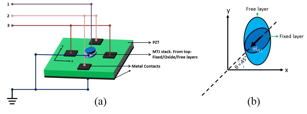
An s-MTJ is a standard MTJ (fixed layer-spacer-free layer) with one difference. The free layer is a magnetostrictive nanomagnet in elastic contact with an underlying poled piezoelectric thin film of thickness as shown in Fig. 1(a). Square electrodes of edge (), separated by a distance (), are delineated on the piezoelectric surrounding the MTJ stack. The bottom of the conducting substrate is grounded. The electrode ‘1’ is used to read the s-MTJ resistance by passing a current to ground. Application of a voltage across the piezoelectric film using the electrode pair ‘2’ shown in Fig. 1(a) generates biaxial strain in the film (compresssion along the line joining the electrode pair and tension perpendicular to it, or vice versa, depending on the polarity of the voltage), which is partially or fully transferred to the soft layer of the s-MTJ in elastic contact with the film. This rotates its magnetization via the Villari effect cui1 ; cui2 ; cui3 and changes the s-MTJ resistance, realizing the action of a switch. A tiny amount of voltage (few mV) is required to rotate the magnetization through a large angle and change the s-MTJ resistance substantially if the piezoelectric film is 100 nm thick, resulting in a switching energy dissipation ( = capacitance associated with charging the piezoelectric, which is 1-2 fF) of a few tens of aJ hasnain ; noel . The internal energy dissipation within the magnetostrictive free layer due to Gilbert damping is negligible kuntal1 .
The s-MTJ operation has been experimentally demonstrated li ; wang . Here, we first show that an s-MTJ can be engineered to produce very unusual device characteristics and then show that such device characteristics elicit TCAM behavior.
Consider a “skewed” s-MTJ where the major axes of the fixed and free layers subtend an angle of 45∘ between them as shown in Fig. 1(b). The fixed layer is implemented with a synthetic anti-ferromagnet (SAF) to reduce the dipole interaction with the free layer, but not completely eliminate it. Because of shape anisotropy, the magnetization orientations of both layers will lie along the respective major axes of the ellipses, but owing to the remanent dipole interaction, the angle between them will be obtuse rather than acute (see Fig. 1(b)). When the free layer is strained by the voltage applied at the electrode pairs ‘2’, its magnetization begins to rotate. The remanent dipole interaction, will make it rotate clockwise in Fig. 1(b) so as to always increase the angular separation between the magnetizations of the two layers. We have simulated the magnetization rotation under strain in the presence of thermal noise using stochastic Landau-Lifshitz-Gilbert (s-LLG) simulations (see later description). Out of 106 switching trajectories simulated, not a single one rotated anti-clockwise, showing that the clockwise rotation is overwhelmingly preferred.
Strain can usually rotate magnetization by up to 90∘ (from the major to the minor axis of the ellipse) although larger rotations are possible under special circumstances kuntal_sci_rep ; ayan_apl . Initially, before the application of strain, the magnetizations of the fixed and free layers subtend an angle = 135∘ as shown in Fig. 1(b). Upon application of strain, the magnetization begins to rotate clockwise and gradually increases from 135∘ to 225∘. The MTJ resistance depends on according to camsari
| (1) |
where is the MTJ resistance when the magnetizations of the fixed and free layers are parallel (anti-parallel), is the resistance when the angular separation between the magnetizations is , and . Since varies between 135∘ and 225∘, the conductance of the MTJ (or current flowing through terminal ‘1’ at a fixed bias) plotted as a function of the voltage applied at terminal ‘2’ (which generates the rotation) will exhibit a “valley”. The bottom of the valley corresponds to when the MTJ resistance becomes maximum.
We can alter the stress distribution in the free layer of the s-MTJ by applying an additional voltage across the piezoelectric with a third pair of electrodes ‘3’ shown in Fig. 1(a). This will allow us to shift the position of the valley bottom in the transconductance characteristic versus ( is the current through the -th terminal at a fixed bias and is the voltage applied at the -th terminal). Thus, we have a 4-terminal switch with terminals ‘1’, ‘2’, ‘3’ and ground, where the current between ‘1’ and ground is changed with a voltage applied to ‘2’ and the transfer characteristic associated with this change can be modulated with a voltage applied at terminal ‘3’.
When both electrode pairs ‘2’ and ‘3’ are activated, the strain distribution in the piezoelectric (and hence in the free layer of the s-MTJ) becomes complex. Exact strain profiles can be calculated with three dimensional finite element analysis (e.g. with COMSOL Multiphysics package) as in cui1 ; wang , but in order to keep the analysis tractable, we will assume that activating an electrode pair generates only uniaxial stress along the line joining that pair. Note that if anything, this over-estimates the stress required to produce a given rotation , and is hence conservative. The sign of the uniaxial stress (tensile or compressive) depends on the polarity of the voltage. If we activate electrode pair ‘2’, then we will generate uniaxial stress along the major axis of the elliptical free layer of the s-MTJ (compressive or tensile depending on the voltage polarity at ‘2’), whereas if we activate electrode pair ‘3’ we will generate uniaxial stress along the minor axis of the free layer. We have assumed that the free layer is made of Terfenol-D which has a positive and large magnetostriction coefficient (900 ppm). Compressive stress along any direction in the free layer will rotate its magnetization away from that direction (maximum rotation is 90∘) while tensile stress will keep it aligned along that direction. This allows us to control the angle with voltages at ‘2’ and ‘3’.
We have computed versus the voltage (assuming = 0) at 0 K temperature (no thermal noise) using the Landau-Lifshitz-Gilbert equation which yields the magnetization orientation of the free layer as a function of time under the influence of voltage generated stress:
| (2) |
where is the saturation magnetization of the free layer material, is the gyromagnetic ratio, is the Gilbert damping constant in the free layer, and is the effective magnetic field experienced by the free layer at any time and is given by
| (3) |
where is the (constant) dipole field exerted by the fixed layer, is the field due to shape anisotropy, is the field generated by stress, and is the random field due to thermal noise. Expressions for these fields are given in ref. salehi1 ; kuntal2 . Stress is generated in the piezoelectric substrate by activating a shorted electrode pair with a voltage . The resulting stress is assumed to be uniaxial along the line joining the centers of the electrodes in the activated pair. The voltage generates a vertical electric field of in the piezoelectric substrate. Following Cui, et al. cui1 , we will assume that a vertical electric field of 37 kV/m is required to produce a uniaxial stress of 1 MPa in the substrate along the line joining the electrodes in the activated pair. This stress is assumed to be fully transferred to the soft magnetic layer of the MTJ resting on top of the substrate. A negative voltage generates tensile stress and a positive voltage compressive stress because of the direction in which the piezoelectric film has been poled. Equation (2) is solved for various -s until steady state is reached and that yields the orientation of the free layer’s magnetization as a function of the -s and hence versus for a fixed . This result is plotted in Fig. 2 (a) for 0 K and 300 K tempatures, assuming = 0 V and directed along the major axis of the fixed layer. The dispersion in the 300 K result is due to thermal noise. The parameters assumed for the free layer (material Terfenol-D) are given in Table I. For the MTJ, we assumed the spacer layer to be made of MgO of thickness 1 nm. For this thickness, the resistance-area product of the MTJ is about 10 - isogami . If the thickness is increased to 2 nm, the resistance-area product increases to 8000 -.
| Saturation magnetization () | 8 A/m |
|---|---|
| Major axis dimension | 80 nm |
| Minor axis dimension | 60 nm |
| Thickness | 15 nm |
| Magnetostriction coefficient | 900 ppm |
| Gilbert damping constant | 0.1 |
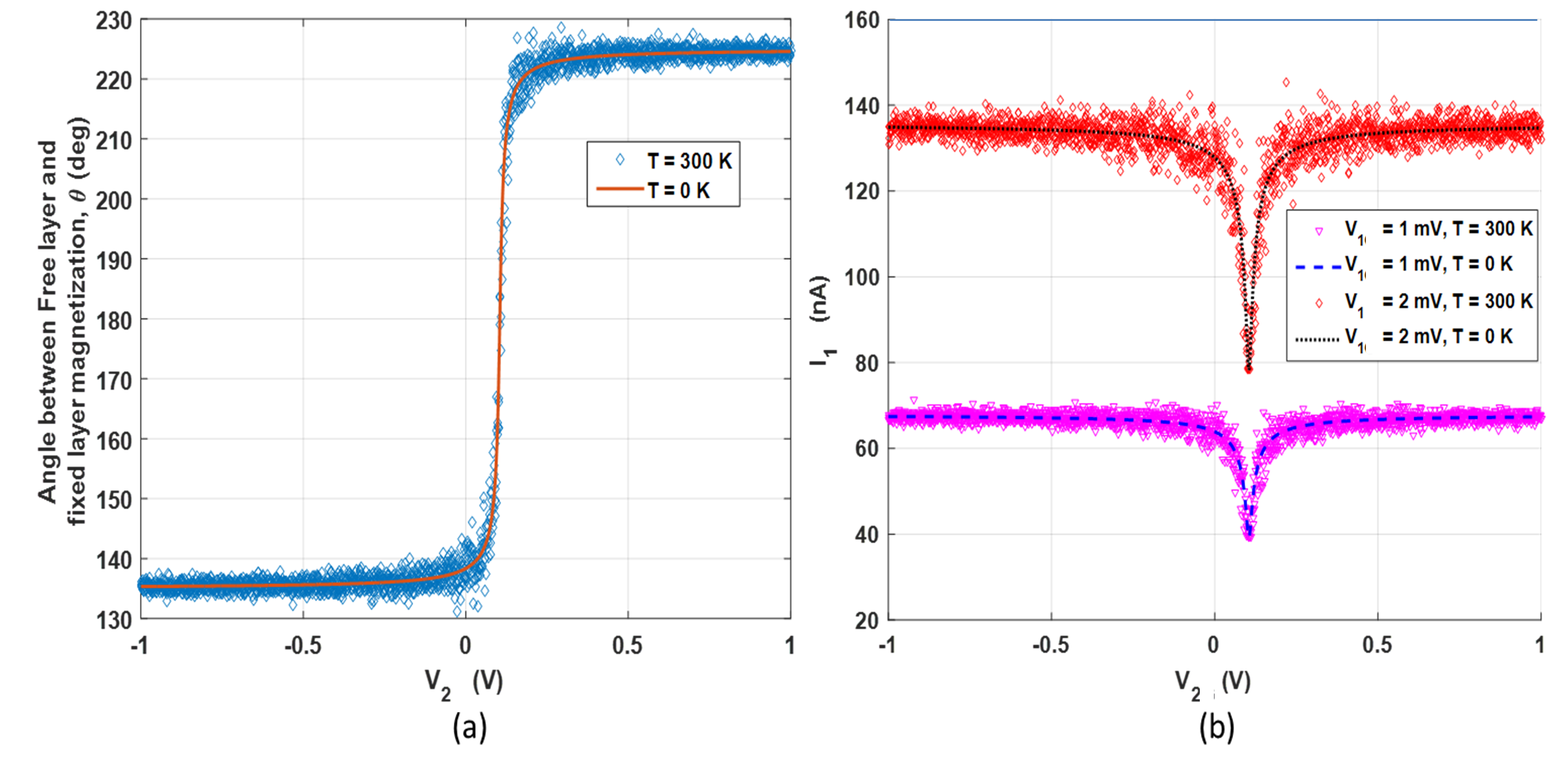
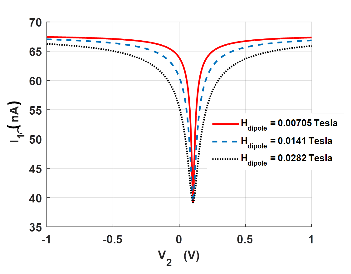
We then use Equation (1) to extract the s-MTJ resistance versus from the versus realtion in Fig. 2(a) and plot the transfer characteristic versus (at 0 K and 300 K temperatures) in Fig. 2(b) for two different values of . Note that this characteristic has a notch or valley. Note also that there is no significant difference between the 0 K and (average of) 300 K results. Therefore, in the rest of this paper, we will present the 0 K results, noting that the 300 K results will not be significantly different. In Fig. 3, we show how the transfer characteristics depend on the dipole field strength, assuming that the temperature is 0 K.
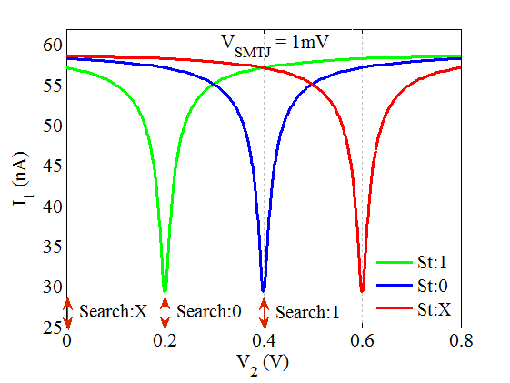
In Fig. 4, we plot the transfer characteristic versus at 0 K temperature for three different values of . Clearly, the position of the notch can be shifted around with the voltage which generates an additional uniaxial stress (negative voltage tensile and positive voltage compressive) along the line joining the electrode pads ‘3’. This makes it a 4-terminal switch.
III s-MTJ-based Dynamic TERNARY CONTENT ADDRESSABLE MEMORY (TCAM)
In a skewed s-MTJ, the current between the free and fixed layers can be controlled by the gate voltages at and [Fig. 4]. At any given value of , is lowest when and ‘match’, meaning that they obey the relation , where is a fixed voltage that we call the ‘offset voltage’. The current increases steeply when and deviate from the ‘match’ condition. Therefore, the current through skewed s-MTJ characterizes similarity between the gate voltages and . Moreover, a current-based similarity index in skewed s-MTJ is suitable for an easier inter-cell aggregation and for evaluating similarity between large scale vectors/patterns. When multiple skewed s-MTJs are arranged in parallel, the column current aggregates the similarity index (i.e., the s-MTJ current ) from each cell. Therefore, the column current evaluates similarity between two vectors/patterns, each applied at the and nodes of the column, respectively. We have exploited this associative processing capability of s-MTJ in TCAM design.
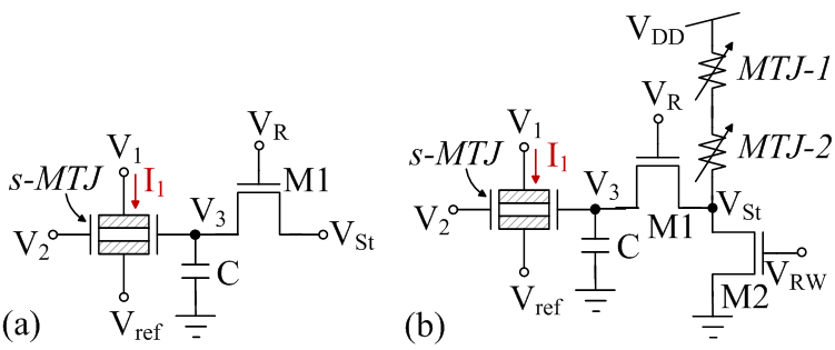
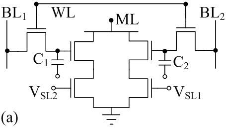
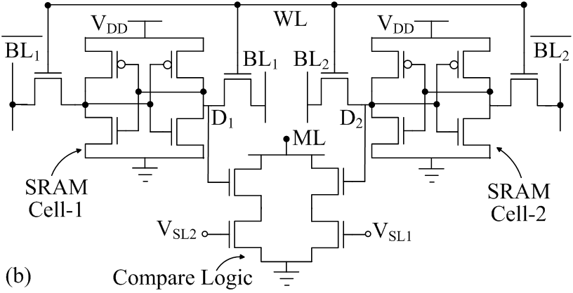
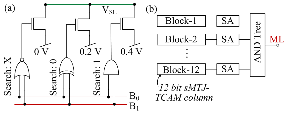
Fig. 4 discusses the encoding scheme for implementing match operation of a TCAM cell through a single skewed s-MTJ. In Fig. 4, s-MTJ current () is shown at varying search bit potentials (i.e., potential) and at varying stored bits (i.e., potential). The search bits ‘X’, ‘0’, and ‘1’ are encoded as 0 V, 0.2 V, and 0.4 V, respectively. The store bits ‘1’, ‘0’, and ‘X’ center the valley peak to 0.2 V, 0.4 V, and 0.6 V, respectively. In the encoding scheme, a high s-MTJ current (i.e., a lower resistance in the s-MTJ) indicates a match between the stored and search bit. If the stored bit in a cell is ‘X’, current through the s-MTJ is high at all search bits ‘0’, ‘1’ & ‘X’, thereby ignoring (masking) the search bit. Similarly, when the search bit is ‘X’, a high current is induced in the s-MTJ indicating a match irrespective of the stored bit. Therefore, the skewed s-MTJ significantly reduces the complexity of match operation in a TCAM.
The cell schematics for an s-MTJ-based dynamic TCAM is shown in Fig. 5(a). The cells exploit high parasitic capacitance at node for a dynamic storage of the storage bit. Note that the capacitance at is high due to an underlying high dielectric constant ( 1000) piezoelectric layer. The parasitic capacitance can be further enhanced by thinning down the piezoelectric layer, and/or by increasing the contact area of electrode atop the piezoelectric layer. The parasitic capacitance is charged through the access NMOS transistor M1. The cell in Fig. 5(b) supports local refresh of the storage bit, i.e., the storage potential is generated within the cell using MTJ-1, MTJ-2, and M2. MTJ-1 and MTJ-2 are standard MTJs (not skewed) and can be switched by spin polarized current generating spin transfer torque or domain wall motion. MTJs locally store the storage bit and refresh the storage potential at node when read and access transistors (M1 & M2) are activated. Both MTJs are programmed at high resistance () to store ‘1’ and both at low resistance () to store ‘X’. One of the MTJs is programmed at and the other at to store ‘0’. The MTJs are designed such that MTJ-2 has a slightly higher critical switching current () than MTJ-1. To program both MTJs at low resistance, a positive programming voltage magnitude is applied at the node [Fig. 5(b)]. To program both MTJs at high resistance, programming voltage polarity is reversed from the previous case (i.e., a negative ). To write MTJ-1 at and MTJ-2 at , first both MTJs are programmed at . Then a programming pulse of negative polarity whose width is greater than the switching time of MTJ-1 but less than the switching time of MTJ-2 is applied at node. Since the critical switching current of MTJ-1 is lower than that of MTJ-2, MTJ-1 switches to while MTJ-2 remains at . The cell in Fig. 5(a) is designed for a global refresh, i.e., refresh potentials are supplied externally to the array (as in a DRAM). Note that a local refresh in Fig. 5(b) does not interfere with the regular search operation, and therefore is useful for improving performance and mitigating the complexity of refresh operation. Meanwhile, the global refresh-based cell in Fig. 5(a) also reduces cell area.
Standard CMOS-based static and dynamic TCAM cells are shown in Fig. 6(a-b) for comparison against the s-MTJ-based TCAM cells. The unconventional characteristic of the s-MTJ greatly reduces the footprint. Note that a standard CMOS-based static TCAM cell requires 16 transistors and a dynamic TCAM cell requires six transistors and two trench capacitors. In contrast, the skewed s-MTJ based design requires a single s-MTJ. Nonvolatile storage in the standard MTJs eliminates standby power dissipation in the TCAM array. A narrow valley in the transfer characteristic of an s-MTJ (see Fig. 4) scales down the required minimum voltage difference between the stored logic ‘0’ and ‘1’, leading to a lower bias current through M1 and lower dynamic power in charging search lines ( capacitance). Moreover, only a single ended search word mapping (unlike CMOS designs) is needed, resulting in lower dynamic power dissipation and lower wiring overheads.
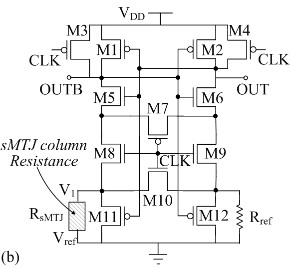
TCAM cells in a column are connected in parallel to form the n-bit search/stored word. A TCAM array constitutes multiple such search columns each storing a word from the database [Fig. 7(a)]. Fig. 7(b) shows the column sense-amplifier schematic comparing the resistance of a s-MTJ-based TCAM column against a reference resistance. Nodes OUT and OUTB in the sense-amplifier are charged to high in the precharge mode (CLK = 0). Transistors M7-M10 equalize the node potential at their source and drain ends when CLK = 0. In the evaluate mode (CLK = 1), if the column resistance due to TCAM cells is lower than the reference resistance (), the current through branch M5-M8 is higher leading to OUT = 1 (Match). Otherwise, OUT = 0 (Mismatch), if the column resistance is higher.
The reference resistance is configured such that it has a resistance in between the ‘worst case match’ and the ‘worst case one-bit mismatch’. For an n-bit search word, the ‘worst case match’ column resistance obeys the relation
| (4) |
where is the worst case match resistance in an s-MTJ-based TCAM cell. Note that for a match in the TCAM cell, the match resistance () in s-MTJ follows for any combination of ternary bits: 0, 1, and X. Meanwhile, the ‘worst case one-bit mismatch’ column resistance obeys the relation
| (5) |
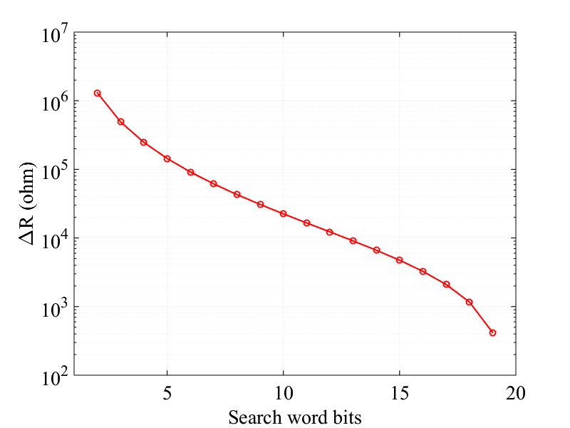
where is the best case match resistance in an s-MTJ-based TCAM cell, and is the mismatch resistance. Note that in case of a mismatch, the mismatch resistance is always for any combination of ternary bits: 0, 1, and X. Figure 8 plots differential resistance between the ‘worst case match’ and the ‘worst case one-bit mismatch’, i.e., at varying search word size (). Note that for . Thus, the s-MTJ characteristics limit the maximum number of TCAM cells in a column. The maximum number of parallel cells in a column can be increased by enhancing peak to valley resistance in s-MTJ (i.e., ) and/or enhancing sharpness of the valley (i.e., by minimizing ). Nonetheless, large size search words can still be processed using s-MTJ-based TCAM cells by combining multiple block through an AND-tree as shown in Fig. 9(b), albeit at the cost of increasing peripheral area and power.
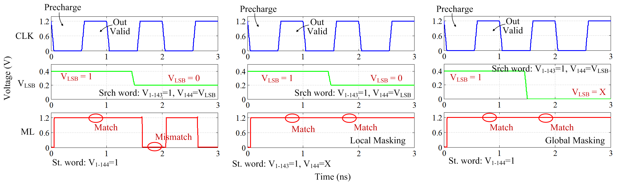
Operational waveforms for the TCAM array are shown in Fig. 10. At CLK = 0, the search bits and are decoded to search bit potential (0, 0.2, or 0.4 V depending on the search bit being ‘X’, ‘0’, or ‘1’, respectively) using circuitry shown in Fig. 9(a). At CLK = 1, column peripherals in each block determine a match or mismatch and the following AND-tree combines their outputs to determine an n-bit (full length) match. Fig. 10 shows simulated transient of the TCAM array for a 144-bit search operation. As indicated in Fig. 10(a), the output (ML) is high in the case of a match between the search word and stored word, and ML becomes low with mismatch. Fig. 10(b) shows the case of a don’t care (‘X’) in the least significant bit (LSB) of the stored word. Therefore, in the search operation ML is high regardless of the LSB in search word (local masking). Similarly, when the search bit is ‘X’, Fig. 10(c) shows a match irrespective of the corresponding stored bit (global masking).
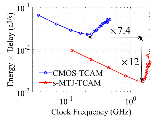
In Fig. 11, at varying operational frequencies, the energy-delay-product (EDP) of the proposed s-MTJ-based dynamic TCAM is compared against that of CMOS-based dynamic TCAM. The energy-efficiency of s-MTJ-based TCAM is remarkably higher than that of CMOS-TCAM. Owing to a much more simplified cell and search operation, the minimum energy-delay product (EDP) is 12 smaller than the minimum EDP in CMOS-TCAM. Furthermore, while the operational frequency of CMOS-based TCAM is limited, the s-MTJ-based TCAM delivers a significantly improved performance. Note that the minimum EDP in s-MTJ-based TCAM occurs at 7 higher frequency than the minimum EDP frequency in CMOS-TCAM. At an operational frequency of 1 GHz, the EDP in sMTJ-based TCAM is 100 smaller than that in CMOS-TCAM. As interest in data-intensive and search-driven platforms (such as BigData) grows, the unique characteristics of an s-MTJ based TCAM will become increasingly important to reduce energ-delay product in such systems.
IV CONCLUSIONS
This work has shown that the unique characteristics of a skewed s-MTJ can significantly simplify TCAM design and operation. In a skewed s-MTJ, the MTJ resistance can be controlled by the gate voltages and . The resistance of an s-MTJ becomes maximum when and ‘match’, i.e., they differ only by a fixed amount which we have called the ‘offset’. This associative property of the skewed s-MTJ enabled us to design a single s-MTJ-based match operation in a TCAM cell. The s-MTJ-based cell is minimized to one access transistor and one s-MTJ for a dynamic TCAM with global refresh. The cell is minimized to two transistors, two MTJs and one s-MTJ for dynamic TCAM with local refresh. The dynamic TCAM with local refresh has higher performance at the cost of slightly higher cell area. In the explored TCAM cell, the operation is non-Boolean and single ended which also minimizes dynamic power and routing. The s-MTJ-based cell shows 12 lower minimum energy-delay product (EDP) than CMOS-based cell. Moreover, the frequency at minimum EDP in the discussed cell is 7 higher than the frequency of minimum EDP in CMOS-based TCAM.
Acknowledgement
The work at Virginia Commonwealth University was supported by the US National Science Foundation under grant ECCS-1124714 and by the State of Virginia through the Research Commercialization Fund administered by the Center for Innovative Technology.
References
References
- (1) G. E. Moore, “Cramming more components onto integrated circuits”, Electronics Magazine, p. 4 (1965).
- (2) K. Roy, S. Bandyopadhyay and J. Atulasimha, “Hybrid spintronics and straintronics: A magnetic technology for ultralow energy computing and signal processing”, Appl. Phys. Lett., 99, 063108 (2011).
- (3) K. Roy, S. Bandyopadhyay and J. Atulasimha, “Energy dissipation and switching delay in stress-induced switching of multiferroic nanomagnets in the presence of thermal fluctuations”, J. Appl. Phys., 112, 023914 (2012).
- (4) M. Salehi-Fashami, K. Roy, J. Atulasimha and S. Bandyopadhyay, “Magnetization dynamics, Bennett clocking and associated energy dissipation in multiferroic logic”, Nanotechnology, 22, 155201 (2011).
- (5) M. Salehi-Fashami, J. Atulasimha and S. Bandyopadhyay, “Magnetization dynamics, throughput and energy dissipation in a universal multiferroic nanomagnetic logic gate with fan-in and fan-out”, Nanotechnology, 23, 105201 (2012)
- (6) M. Salehi-Fashami, J. Atulasimha and S. Bandyopadhyay, “Energy dissipation and error probability in fault-tolerant binary switching”, Sci. Rep., 3, 3204 (2013).
- (7) K. Munira, Y. K. Xie, S. Nadri, M. B. Forgues, M. Salehi-Fashami, J. Atulasimha, S. Bandyopadhyay and A. W. Ghosh, “Reducing error rates in straintronic multiferroic nanomagnetic logic by pulse shaping”, Nanotechnology, 26, 245202 (2015).
- (8) M. Salehi-Fashami, K. Munira, S. Bandyopadhyay, A. W Ghosh and J. Atulasimha, “Switching of dipole-coupled multiferroic nanomagnets in the presence of thermal noise: Reliability of nanomagnetic logic”, IEEE Trans. Nanotechnol., 12, 1206-1212(2013).
- (9) M. M. Al-Rashid, S. Bandyopadhyay and J. Atulasimha, “Dynamic error in strain-induced magnetization reversal of nanomagnets due to incoherent switching and formation of metastable states: A size-dependent study”, IEEE Trans. Elec. Dev., 63, 3307-3313 (2016).
- (10) M. M. Al-Rashid, D. Bhattacharya, S. Bandyopadhyay and J. Atulasimha, “Effect of nanomagnet geometry on reliability, energy dissipation and clock speed in strain-clocked DC-NML”, IEEE Trans. Elec. Dev., 62, 2978-2986 (2015).
- (11) A. K. Biswas, J. Atulasimha and S. Bandyopadhyay, “An error-resilient non-volatile magneto-elastic universal logic gate with ultralow energy-delay product”, Sci. Rep., 4, 7553 (2014).
- (12) S. Khasanvis, M. Y. Li, M. Rahman, M. Salehi-Fashami, A. K. Biswas, J. Atulasimha, S. Bandyopadhyay and C. A. Moritz, “Self-similar magneto-electric nanocircuit technology for probabilistic inference engines”, IEEE Trans. Nanotechnol. 14, 980-991 (2015).
- (13) S. Khasanvis, M. Y. Li, M. Rahman, A. K. Biswas, M. Salehi-Fashami, J. Atulasimha, S. Bandyopadhyay and C. A. Moritz, “Architecting for causal intelligence at nanoscale”, Computer, 48, 54-64 (2015).
- (14) N.-F. Huang, W.-E. Chen, J.-Y. Luo, and J.-M. Chen, ”Design of multi-field IPv6 packet classifiers using ternary CAMs,” in Global Telecommunications Conference, 2001. GLOBECOM’01. IEEE, 2001, pp. 1877-1881.
- (15) S. Panchanathan and M. Goldberg, ”A content-addressable memory architecture for image coding using vector quantization,” IEEE Transactions on Signal Processing, vol. 39, pp. 2066-2078, 1991.
- (16) M. Meribout, T. Ogura, and M. Nakanishi, ”On using the CAM concept for parametric curve extraction,” IEEE Transactions on Image Processing, vol. 9, pp. 2126-2130, 2000.
- (17) M. Nakanishi and T. Ogura, ”Real-time CAM-based Hough transform algorithm and its performance evaluation,” Machine Vision and Applications, vol. bf 12, pp. 59-68, 2000.
- (18) D. Kudithipudi and E. John, ”On estimation of static power-peformance in TCAM,” in 2008 51st Midwest Symposium on Circuits and Systems, 2008, pp. 783-786.
- (19) J. Cui, J. L. Hockel, P. K. Nordeen, D. M. Pisani, C-y Liang, G. P. Carman and C. S. Lynch, “A method to control magnetism in strain-mediated magnetoelectric islands”, Appl. Phys. Lett., 103, 232905 (2013).
- (20) C-y Liang, S. M. Keller, A. E. Sepulveda, W-Y Sun, J. Cui, C. S. Lynch and G. P. Carman, “Electrical control of a single magnetoelastic domain structure on a clamped piezoelectric thin film - analysis” J. Appl. Phys., 116, 123909 (2014).
- (21) J. Cui, C-y Liang, E. A. Paisley, A. Sepulveda, J. F. Ihlefeld, G. P. Carman and C. S. Lynch, “Generation of localized strain in a thin film piezoelectric to control individual magnetoelectric heterostructures”, Appl. Phys. Lett., 107 092903 (2015),
- (22) H. Ahmad, J. Atulasimha and S. Bandyopadhyay, “Reversible strain-induced magnetization switching in FeGa nanomagnets: Pathway to a rewritable, non-volatile, non-toggle, extremely low-energy straintronic memeory”, Sci. Rep., 5, 18264 (2015).
- (23) N. D’Souza, M. Salehi-Fashami, S. Bandyopadhyay and J. Atulasimha, “Experimental clocking of nanomagnets with strain for ultralow power Boolean logic”, Nano Letters, 16, 1069-1075 (2016).
- (24) P. Li, A. Chen, D. Li, Y. Zhao, S. Zhang, L. Yang, Y. Liu, M. Zhu, H. Zhang and X. Han, “Electric field manipulation of magnetization rotation and tunneling magnetoresistance of magnetic tunnel junctions at room temperature”, Adv. Mater., 26, 4320 (2014).
- (25) Z. Zhao, M. Jamali, N. D’Souza, D. Zhang, S. Bandyopadhyay, J. Atulasimha and J-P. Wang, “Giant voltage manipulation of MgO-based magnetic tunnel junctions via localized ansitropic strain: A potential pathway to ultra-energy-efficient memory technology”, Appl. Phys. Lett., 109, 092403 (2016).
- (26) K. Roy, S. Bandyopadhyay and J. Atulasimha, “Binary switching in a ’symmetric’ potential landscape”, Sci. Rep., 3, 3038 (2013).
- (27) A. K. Biswas, S. Bandyopadhyay and J. Atulasimha, “Complete magnetization reversal in a magnetostrictive nanomagnet with voltage-generated stress: A reliable energy-efficient non-volatile magneto-elastic memory”, Appl. Phys. Lett., 105, 072408 (2014).
- (28) K. Y. Camsari, S. Ganguly and S. Datta, “Modular approach to spintronics”, Sci. Rep., 5, 10571 (2015).
- (29) S. Isogami, M. Tsunoda, K. Komagaki, K. Sunaga, Y. Uehara, M. Sato, T. Miyajima and M. Takahashi, “In-situ heat treatment of ultrathin MgO layer for giant magnetoresistance ratio with low resistance-area product in CoFeB/MgO/CoFeB magnetic tunnel junctions”, Appl. Phys. Lett., 93, 192109 (2008).