Spin injection and detection up to room temperature in Heusler alloy/n-GaAs spin valves
Abstract
We have measured the spin injection efficiency and spin lifetime in Co2FeSi/n-GaAs lateral nonlocal spin valves from 20 to 300 K. We observe large (40 V) spin valve signals at room temperature and injector currents of A/cm2, facilitated by fabricating spin valve separations smaller than the 1 m spin diffusion length and applying a forward bias to the detector contact. The spin transport parameters are measured by comparing the injector-detector contact separation dependence of the spin valve signal with a numerical model accounting for spin drift and diffusion. The apparent suppression of the spin injection efficiency at the lowest temperatures reflects a breakdown of the ordinary drift-diffusion model in the regime of large spin accumulation. A theoretical calculation of the D’yakonov-Perel spin lifetime agrees well with the measured n-GaAs spin lifetime over the entire temperature range.
I Introduction
All-electrical spin transport has been demonstrated in III-V semiconductors Lou et al. (2007); Ciorga et al. (2009); Salis et al. (2010); Saito et al. (2013), group IV semiconductors Appelbaum et al. (2007), and in 2D materials such as graphene Tombros et al. (2007); Han et al. (2010). One of the most mature systems studied in the field of semiconductor spintronics is the ferromagnet (FM)/n-GaAs lateral spin valve (SV) structure Lou et al. (2007); Ciorga et al. (2009); Salis et al. (2010). GaAs-based devices have served as a testbed for several seminal semiconductor (SC) spin transport measurements, such as the Hanle effect Lou et al. (2007, 2006), the spin Hall and inverse spin Hall effects Kato et al. (2004); Werake et al. (2011); Garlid et al. (2010), and nuclear hyperfine effects Lou et al. (2006); Chan et al. (2009); Awo-Affouda et al. (2009); Salis et al. (2009). The Dresselhaus spin-orbit interaction (SOI) Dresselhaus (1955) originating from the non-centrosymmetric lattice of III-V SCs makes them attractive candidates for modulation of spin transport using the SOI Datta and Das (1990). At the same time, however, the Dresselhaus SOI present in III-V SCs leads to efficient spin relaxation in the diffusive transport regime.
Electron spin relaxation in n-GaAs at doping levels near the metal-insulator transition is governed by the D’yakonov-Perel (DP) mechanism D’yakonov and Perel’ (1971); Dzhioev et al. (2002). The DP spin relaxation rate in III-V semiconductors has a characteristic behavior D’yakonov and Perel’ (1971); Pikus and Titkov (1984), where is the carrier energy. The spin lifetime is the inverse of the spin relaxation rate. At temperatures for which the carriers are nondegenerate (), the spin lifetime falls sharply as Kikkawa and Awschalom (1998). Short spin lifetimes ( ps) have therefore challenged n-GaAs SV room temperature performance Saito et al. (2013), as the short spin lifetime limits the steady-state spin accumulation.
In this article we demonstrate electrical detection of nonlocal spin accumulation in Heusler alloy FM/n-GaAs lateral spin valve devices up to room temperature. Clear nonlocal SV signals are measured by fabricating devices with injector-detector contact separations of less than a spin diffusion length and applying a forward bias voltage to the detector contact. We use the injector-detector contact separation dependence of the SV signal to extract the n-GaAs spin lifetime and FM/SC interface spin injection efficiency from 20 K up to room temperature. These data allow for a comprehensive and quantitative evaluation of the temperature-dependent performance of FM/n-GaAs lateral SV devices. We find that the spin lifetime in the n-GaAs channel is in quantitative agreement with a theoretical calculation of the DP spin lifetime over the entire temperature range. At low temperatures, we achieve a spin accumulation that is a significant fraction of the carrier density in the channel. This is accompanied by an apparent downturn in the injection efficiency which we believe is due to breakdown of the ordinary drift-diffusion model in the regime of large spin-dependent electrochemical potential splitting.
II Methods
II.1 Structure growth and device fabrication
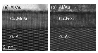
The devices used in this study were fabricated from heterostructures grown by molecular-beam epitaxy (MBE). A 2.5 m Si-doped ( cm-3) GaAs epilayer was grown following a 500 nm undoped GaAs buffer layer grown on a semi-insulating (001) GaAs substrate. To thin the naturally occurring Schottky depletion layer and provide a tunnel barrier for efficient spin injection Rashba (2000); Fert and Jaffrès (2001); Hanbicki et al. (2001), the doping level was increased at the FM/SC interface. A 15 nm transitional doping layer was grown ( cm cm-3) on top of the n-GaAs epilayer, followed by an 18 nm thick heavily doped ( cm-3) layer. Following the GaAs MBE growth, the sample was cooled to 400∘ C under As4-flux at which point the As4-flux was turned off. This resulted in a highly ordered GaAs(001)c(4x4) As-rich surface reconstruction as confirmed by reflection high-energy electron diffraction (RHEED) and in situ scanning tunneling microscopy (STM). For the 5 nm thick epitaxial Heusler film growth, the samples were transfered to a separate growth chamber while maintaining ultra-high vacuum (UHV). The Heusler film growth was performed at 270∘ C with codeposition from individual elemental sources. The Heusler compounds grow with a cube-on-cube orientation with Heusler(001)110 GaAs(001)110Hashimoto et al. (2005); Hirohata et al. (2005). During Heusler growth RHEED was used to confirm layer-by-layer growth of a single crystal film. Cross-sectional high-angle annular dark field scanning transmission electron microscopy (HAADF-STEM) was performed, and example images of the interfaces are shown in Fig. 1. These images confirm the samples are single crystals with mixed L21 and B2 phases in both Co2MnSi (Fig. 1(a)) and Co2FeSi (Fig. 1(b)) films, and a degree of intermixing at the GaAs/Heusler interface of no more than 4-6 atomic layers. The GaAs(001)/Heusler interface resulted in a uniaxial magnetic anisotropy yielding an easy axis along the GaAs [110] direction Hashimoto et al. (2005); Liu et al. (2014, 2016) for both the Co2FeSi and Co2MnSi films.
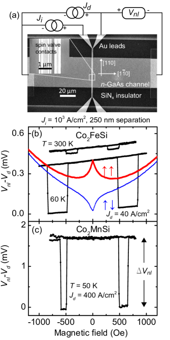
The heterostructures were patterned into lateral spin valve devices using a top-down fabrication process. A combination of electron-beam lithography and photolithography was used, with Ar+ ion milling to define the ferromagnetic contacts and wet etching to define the n-GaAs channel. A silicon nitride insulating layer was deposited by plasma-enhanced chemical vapor deposition (PECVD) and patterned by lift-off to electrically isolate the evaporated Ti/Au vias and bonding pads from the substrate and n-GaAs channel sidewalls. A micrograph of a SV device is shown in Fig. 2(a). The channel width in the GaAs [110] direction is 80 m, the SV contact length is 50 m, the injector width is 1 m, and the detector width is 0.5 m. The large aspect ratio of the SV contacts along the magnetic easy axis was chosen in order to minimize fringe magnetic fields as well as to define a two-dimensional geometry conducive to modeling (channel width spin diffusion length). The large-area remote contacts share the same composition as the SV contacts. The remote contacts, however, have no impact on the SV measurement, because they are placed many spin diffusion lengths away from the SV contacts. Multiple SV devices were fabricated on the same chip by wet etching through the 2.5 m n-GaAs to isolate the devices electrically. SV devices on the same chip were patterned with injector-detector edge-to-edge separations ranging from 250 nm to 5 m.
II.2 Charge transport
Standard multiprobe dc transport measurements were performed as a function of temperature to characterize both the n-GaAs channel and the Co2FeSi/n-GaAs interface. A companion Hall bar was fabricated from the same heterostructure used to fabricate the SV devices, and transport measurements were performed from 10-350 K to extract the carrier concentration and mobility of the n-GaAs. The Hall carrier concentration was measured to be cm-3 for the Co2FeSi heterostructure and cm-3 for the Co2MnSi heterostructure. Fig. 3(a) shows the channel electron mobility and diffusion constant as a function of temperature for the Co2FeSi heterostructure. The Hall factor Yu and Cardona (1996), which causes deviation of the Hall mobility from the electron mobility in n-GaAs, is accounted for by assuming the Hall factor is unity at 300 K Benzaquen et al. (1986); Lewis and Sondheimer (1955) and that the carrier concentration is temperature-independent.
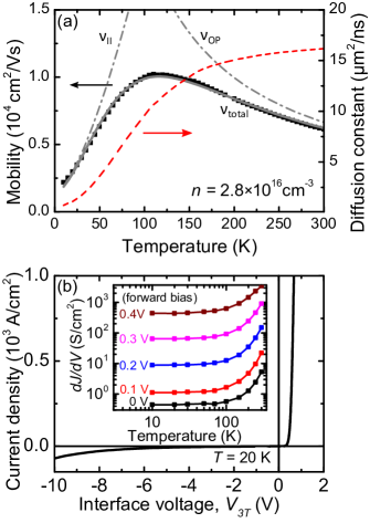
A typical SV device Co2FeSi/n-GaAs contact three-terminal (3T) interface current-voltage () characteristic is shown in Fig. 3(b). The inset of Fig. 3(b) shows the differential conductance per unit area () as a function of temperature. Tunneling-dominated transport (field emission) is known to be necessary for spin injection in FM/GaAs Schottky contacts Hanbicki et al. (2003). The existence of tunneling-dominated transport under forward bias at all temperatures is supported by two observations. First, increases exponentially with forward bias voltage at all temperatures, at a rate that is independent of temperature. Because of the triangular Schottky barrier Cowley and Sze (1965), the forward bias voltage across a Schottky interface changes the thickness of the effective potential barrier through which tunneling occurs Stratton (1969); Brinkman et al. (1970). Although thermionic emission and thermionic field emission also lead to an exponential increase of with interface forward bias voltage, the rate for those processes is strongly temperature-dependent, ruling out those mechanisms. Second, at temperatures below the Fermi temperature of the n-GaAs ( 60 K for these samples) the forward bias differential conductance decreases weakly with decreasing temperature. Although at forward bias is temperature-dependent above the Fermi temperature, this does not imply thermionic emission but rather an increase in the tunneling attempt rate due to the nondegeneracy of the n-GaAs Stratton (1969).
II.3 Spin transport
A schematic diagram of the SV measurement is shown in Fig. 2(a). A dc bias current flows through the injector contact and a second bias current flows through the detector contact. The injector and detector current sources share a common remote reference contact. In this article positive currents and interface voltages refer to electron extraction from the channel, i.e., forward bias of the metal/semiconductor Schottky contact. The bias current applied to the detector contact results in a voltage drop over the tunnel barrier, which is the 3T interface voltage of the detector contact. In these devices, a forward bias applied at the detector contact enhances the nonlocal SV signal size compared to an unbiased detector (zero detector bias is the traditional nonlocal SV configuration pioneered by Johnson and Silsbee (1985)). We will henceforth refer to the case of a bias current applied through the detector contact as the biased-detector spin valve (BDSV) measurement. The enhancement in the SV signal size with a bias applied to the detector contact has been observed in prior n-GaAs lateral SV literature on similar heterostructures Crooker et al. (2009); Bruski et al. (2013), and the possible origins will be discussed in detail later in this article.
An applied magnetic field is swept along the FM easy axis to switch the magnetizations of the injector and detector contacts from the parallel to antiparallel configuration, which allows for a definitive measurement of the nonlocal voltage due to spin accumulation. The difference in the nonlocal detector voltage between the parallel and antiparallel contact magnetization states is due to spin accumulation in the semiconductor Johnson and Silsbee (1985) and is given by
| (1) |
where is the majority (minority) spin-resolved carrier density in the GaAs channel, is the electron charge, and is the inverse of the thermodynamic compressibility of the semiconductor. We will refer to as the spin accumulation and as the dimensionless spin polarization throughout this article. The dimensionless detection efficiency parameter characterizes the spin sensitivity of the detection contact Song and Dery (2010) and is a function of the bias voltage. Because of the bias current applied through the detector contact, is not an open circuit nonlocal voltage (or “electromotive force”). The voltage drop over the detector Schottky tunnel barrier contributes an offset , so that
| (2) |
where is the unit vector specifying the magnetization of the injector (detector) contact.
Example BDSV field sweeps are shown in Figs. 2(b) and (c) on SV devices with an injector-detector edge-to-edge separation of 250 nm at an injector bias current of A/cm2. The BDSV measurement on the device with Co2FeSi contacts is shown in Fig. 2(b) at A/cm2, and for the device with Co2MnSi contacts in Fig. 2(c) at A/cm2. The Co2MnSi/n-GaAs contacts exhibited large voltage noise in the nonlocal SV measurements, and the signal-to-noise ratio (SNR) was not adequate for measurements at high temperatures. For this reason, the analysis presented in this article is carried out for measurements on Co2FeSi/n-GaAs devices. At low temperatures, at which the SNR in Co2MnSi/n-GaAs devices was adequate, the SV measurements were quantitatively similar to those on Co2FeSi/n-GaAs devices. A linear background in can result from the Hall effect due to slight misalignment. The slope, which is a weak function of temperature, is subtracted from the data before extracting .
Nonlocal Hanle (NLH) measurements Johnson and Silsbee (1985); Jedema et al. (2002) were also performed in the biased-detector configuration. In the NLH measurement a magnetic field applied perpendicular to the sample plane is used to apply a precessional torque, which, in combination with diffusion, dephases the spin accumulation. In all of the NLH measurements, the applied field was small enough so that the out-of-plane rotation of the contact magnetization decreased the in-plane component of the magnetization by less than 1.5%, which was considered negligible. The NLH measurement could be executed with the injector and detector contacts in either the parallel or antiparallel configuration. In the fitting of the NLH lineshape discussed in Section III.4, the difference of the parallel and antiparallel field sweeps is used.
At cryogenic temperatures, the NLH measurement in n-GaAs is complicated by the strong hyperfine fields due to dynamic nuclear polarization (DNP) Chan et al. (2009); Salis et al. (2009); Pikus and Titkov (1984). Steady-state conditions are difficult to achieve due to long ( seconds) nuclear depolarization timescales, and small misalignments between the applied field and the contact magnetization result in oblique Overhauser fields, which distort the NLH lineshape Chan et al. (2009); Salis et al. (2009). To mitigate the influence of DNP effective fields on the NLH lineshape, a low duty cycle () pulsed current measurement was used for the NLH sweeps at temperatures below 100 K. The current was turned off for 1000 milliseconds, then pulsed on for 5 milliseconds after which the voltage was recorded and the pulse-train repeated. The current rise and fall times were much shorter than the few-millisecond current pulse duration. The pulsed measurement minimizes the nuclear polarization buildup because the current is on for a time much less than the nuclear polarization time Pikus and Titkov (1984). Example NLH data obtained for the 250 nm separation Co2FeSi device at 60 K are shown in Fig. 2(b).
III Results
III.1 Effect of detector bias
We now discuss the effect of detector bias on our SV measurements. First, we note that Crooker et al. (2009) and Bruski et al. (2013) observed similar enhancement of the spin valve signal in the presence of a detector bias current or voltage. Although several mechanisms have been proposed to explain the enhancement in the nonlocal SV signal with detector bias, the enhancement remains poorly understood. At the end of this section, we will return to discuss possible explanations in light of our measurements.
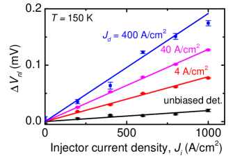
We find that a sufficiently large forward bias current applied through the detector contact increases the SV signal at all temperatures. Fig. 4 shows vs. for the 250 nm separation at 150 K. increases linearly with at all detector bias currents, but the slope of vs. is enhanced with increasing detector forward bias current. This enhancement is particularly advantageous for measurements at high temperatures near 300 K, at which the spin valve signal becomes small in n-GaAs Lou et al. (2007); Saito et al. (2013).
This effect was observed in devices with both Co2FeSi and Co2MnSi contacts and was observed previously for devices with Fe contacts Crooker et al. (2009).
For the case of no bias current passing through the detector (i.e. the conventional nonlocal SV measurement), could be measured in the 250 nm separation device for temperatures less than approximately 200 K (see data points in Fig. 5(b-c) at ). For a fixed injector current, the SV measurement was then performed at different detector bias currents. The corresponding interface voltage drop was measured at each bias current, and so the data may be presented as a function of either bias voltage or current . The results of this measurement at 60 K on the 250 nm separation are shown in Fig. 5(a) and are summarized for all temperatures in Figs. 5(b) and (c). At forward detector bias above interface voltages of 0.2 V, we observe significant enhancement of . As shown in Fig. 5(a), the dependence of on the detector bias is non-monotonic below 200 K, and it is suppressed at small detector voltages (of either sign) and even changes sign for a narrow window of reverse bias. Although is sensitive to 3T signals Lou et al. (2006) produced by local spin injection at the detector contact, only nonlocally-injected spin accumulation contributes to in a spin valve measurement, because is the difference in nonlocal voltage between parallel and antiparallel magnetization states. Furthermore, as shown in Fig. 2(b), the NLH measurement can also be performed with the parallel-antiparallel difference at zero field matching the BDSV magnitude. The existence of the NLH effect at low temperatures demonstrates conclusively that the biased-detector measurement in these devices is a probe of the nonlocally injected spin accumulation.
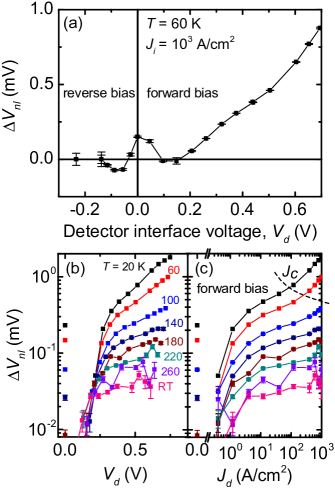
The enhancement in under forward detector bias occurs at all temperatures measured, from 20 K to room temperature. Using the BDSV measurement a clear SV signal could be measured on the separations below 1 m up to and above room temperature on the Co2FeSi devices. To our knowledge, the spin signal we measure on the 250 nm separation device of 40 V at room temperature is over an order-of-magnitude larger than that which has been achieved in FM/n-GaAs SVs, to date Saito et al. (2013). We now discuss the possible origins of the forward bias enhancement of the SV signal.
We consider first the influence of drift due to electric fields in the channel between the injector and detector contacts. Due to the relatively low carrier density in these samples, the spin drift length can be comparable to or larger than the spin diffusion length Yu and Flatté (2002); Tahara et al. (2016). In the case of a forward bias current applied through the detector contact (electron extraction from the channel), the electric field in the channel causes drift of electrons from the injector towards the detector contact, enhancing the nonlocal spin accumulation when compared to spin diffusion alone. To determine if the detector bias current leads to significant drift enhancement of , the current density in the channel between injector and detector contacts at which the spin drift length was equal to the spin diffusion length was evaluated at each temperature. Above a critical current density , which is the current density at which , drift enhancement of the nonlocal spin accumulation below the detector contact becomes significant. The region where this occurs is illustrated in Fig. 5(c), in which the dashed curve shows . The drift enhancement is significant only at low temperatures and the highest detector bias currents. This is in contrast to the case of Si described in Ref. Tahara et al. (2016) in which the long spin lifetime at room temperature, combined with higher current densities than we apply, leads a spin drift length which can be much longer than the spin diffusion length. Because the enhancement in occurs at all temperatures and for current densities far below , it cannot be attributed solely to spin drift effects in the channel. Although variations on simple drift models have been proposed Chantis and Smith (2008), it is unlikely that drift alone can play a significant role given that the enhancement is observed up to room temperature. For the purposes of discussion, we attribute the enhancement in with detector forward bias primarily to enhancement of , the detection efficiency, which we treat as a purely interfacial property. The detection efficiency is a function of detector bias, i.e. .
Hu et al. (2011) and Salis et al. (2010) observed a highly non-monotonic behavior of the sign of the injected spin polarization in similar heterostructures with Fe contacts. The sign and magnitude depended strongly on the details of the n-GaAs band structure in the region of doping near the interface. It is possible that the enhancement of under forward bias is due to the enhanced participation of additional quantum well states that form on the SC side of the tunnel barrier due to the doping layer. It has been proposed that these states play a critical role in both charge and spin current in tunnel contacts using Schottky barriers through FM/SC wavevector-matching arguments which depend on the degree of quantum confinement of the SC states Dery and Sham (2007).
Another point of view focuses on the nonlinear current-voltage characteristic of the tunnel barrier itself Pu et al. (2013); Shiogai et al. (2014). A simple analysis suggests that the ratio of the detected voltage to the spin accumulation should be modified by the ratio of the absolute to differential conductance, although Jansen et al. (2015) have noted that this correction factor is in fact an upper bound. In our case, however, we observe an effect that is opposite to that suggested by this argument. is smaller at forward bias voltage than at zero bias, because increases exponentially with .
Because the bias current applied to the detector introduces a 3T offset to , care must be taken to separate signals due to nonlocal spin accumulation from signals of local origin. Surface localized states in tunnel barriers have been at the center of a controversy in the semiconductor spin injection literature because of the influence these states can have on both the magnitude and lineshape of the 3T Hanle measurement Tran et al. (2009). For example, Txoperena et al. (2014) determined that impurity-assisted tunnelling processes can lead to Lorentzian-shaped magnetoresistance effects that mimic the Hanle effect. Also, Jansen et al. (2012) note that in the 3T geometry the change in 3T voltage due to spin accumulation can originate from spin accumulation in interface localized states as well as bulk channel spin accumulation. Our measurement, however, probes the parallel-antiparallel difference in the nonlocal voltage, notwithstanding the bias applied to the detector contact. Although localized states may play an important role in the spin-polarized transport at our interfaces, the mechanisms discussed by Txoperena et al. (2014); Jansen et al. (2012) are only relevant for 3T local spin detection where the ferromagnetic contact simultaneously serves as the injector and detector.
Another possible physical explanation for the detector bias dependence of is that significant features exist in the spin-resolved density-of-states (DOS) of the Co2FeSi/GaAs interface near the Fermi level. These features could lead to spin injection and detection efficiencies that vary with forward bias voltage, as states above the Fermi level in the FM become available for elastic tunnelling from the SC. Density functional theory (DFT) calculations done for Co2FeSi in the L21 phaseWurmehl et al. (2005); Balke et al. (2006) suggest strong variations in the bulk minority DOS near the Fermi level over energy ranges of hundreds of meV, which are comparable to the scale of the interface voltages at the detector in our measurement. Strong bulk minority DOS variations near the Fermi level have also been predicted for Co2MnSi which are largely insensitive to the phase (L21 vs. B2)Picozzi and Freeman (2007). However, the bias dependence of spin detection shown in Fig. 5(a) cannot be clearly correlated with the features in the spin-resolved DOS reported by DFT calculations. Additionally, interface states, such as those which have been proposed for the Fe/GaAs(001) interface, will contribute to the tunneling currentChantis et al. (2007). Although it is likely that the low-voltage features in are associated with electronic structure of the interface, we have no quantitative description of the bias-dependence of the nonlocal voltage.
We now comment briefly on the sign of the spin valve signals we observe. In this article, a decrease in in the antiparallel magnetization state is defined as a positive . The BDSV sweeps shown in Figs. 2(b) and (c) are examples of positive values. The sign of is determined by the relative signs of the injection and detection efficiencies. That is, same sign (opposite sign) injection and detection efficiencies correspond to a positive (negative) . Microscopically, the individual signs of these efficiencies are determined by the difference in the spin-resolved interface conductances , where the “up” direction is defined by the energy-integrated majority spin direction (i.e., magnetization) of the ferromagnet. Because the nonlocal voltage depends on the product of the two efficiencies, it is not possible to correlate its sign directly with the sign of the spin accumulation. At low temperatures, the influence of the electronic Knight field on the nuclear polarization in oblique Hanle geometries Pikus and Titkov (1984); Chan et al. (2009) can be used to determine the sign of the spin accumulation with respect to the magnetization orientation. We have determined that at high forward bias (spin extraction) the sign of the spin accumulation is minority in Co2FeSi and majority in Co2MnSi with respect to the magnetization of the injector contact Christie (2014).
III.2 Injector-detector separation dependence
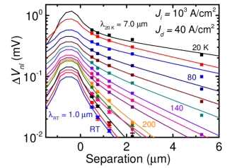
We quantify device parameters at different temperatures using the injector-detector separation dependence (IDSD) of the spin valve signal size, rather than relying on NLH measurements. The NLH measurement in n-GaAs becomes challenging at high temperatures because of the magnetoresistance backgrounds present over the much larger magnetic field range required when the spin lifetime is small. The injector-detector separation was varied in order to extract the spatial dependence of the spin accumulation in the channel. By utilizing the enhanced signal in the BDSV configuration, clear SV signals could be measured at the smallest separations up to room temperature. For the IDSD measurement, the detector contact forward bias was fixed at a current density of 40 A/cm2. This bias current was well into the enhancement regime shown in Fig. 5(c), but below the regime where spin drift enhancements were significant at low temperatures. was recorded at bias conditions A/cm2, A/cm2 for each temperature and injector-detector separation. The results of the IDSD measurement are summarized in Fig. 6. The solid lines in Fig. 6 are fits to a numerical model of the spin accumulation in the channel, which will be explained in detail later in this article.
We note that in Eq. 1, is proportional to the spin accumulation and the inverse compressibility of the channel . At temperatures above the Fermi temperature (in our samples K) at which the n-GaAs is no longer degenerate, is a function of temperature. In the nondegenerate regime ( ), . This relationship implies that as the temperature increases in the nondegenerate regime, a larger is measured for a given spin accumulation. For these samples,
| (3) |
Because of this enhancement factor, while the spin accumulation falls by two orders of magnitude from 20 K to 300 K, at separations much smaller than a diffusion length only decreases by roughly one order of magnitude over the same temperature range.
III.3 Modeling of the spatial decay of spin accumulation
Here we discuss the model used to describe the spin accumulation in the channel and which is used to fit the IDSD measurement results. Typically, in systems where spin diffusion is one-dimensional, the SV signal size is interpreted with the expression Johnson and Silsbee (1985)
| (4) |
where is the channel resistivity, is the channel cross-sectional area, and is injector-detector separation. Eq. 4 has been used to model the SV signal size in a variety of material systems Jedema et al. (2002); Lou et al. (2007); Tombros et al. (2007) in which the FM/NM barrier resistance is much larger than the channel spin resistance, so that the conductivity mismatch problem Rashba (2000) may be ignored. We choose to use a more general numerical model of the spin accumulation in the channel to fit to the IDSD measurement because of several considerations. First, as discussed earlier, drift due to the bias current influences the spatial spin accumulation profile in n-GaAs at low temperatures, and the exact drift field is best captured by a numerical model. Second, at measurement temperatures near room temperature the spin diffusion length in n-GaAs is less than the channel thickness of 2.5 m. In this regime a more general solution of the spin drift-diffusion equation is needed, because Eq. 4 is only appropriate for devices where the spin drift and diffusion are effectively one dimensional. In two or three dimensions, the spin accumulation decays faster than for , in exact analogy to the two and three dimensional solutions of the screened Poisson equation.
The spatial profile of spin accumulation in the channel is modeled by solving the spin drift-diffusion equation Yu and Flatté (2002) in steady state,
| (5) |
where is the dimensionless spin polarization of the channel, is the spin diffusion constant (equal to the charge diffusion constant Yu and Flatté (2002)), specifies the injector contact magnetization direction, and the last term specifies the source term, which is only nonzero at the cells of the finite element model where spin injection occurs. In the source term, the factor in the denominator is the size of the injection cell in the -direction, which normalizes the injection rate in the finite-element grid properly. is the current density in the channel, and the parameter is the spin injection efficiency at the FM/SC interface (i.e. for the spin current at the FM/SC interface is equal to the charge current). encompasses both the bulk polarization of the current in the FM, as well as interface effects determining the polarization of the charge current.
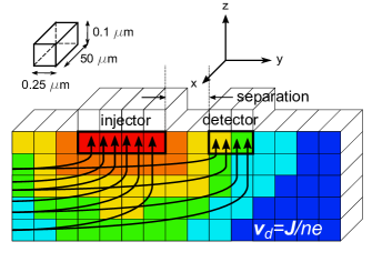
The spin valve device geometry is cast into a finite-element grid, and Eq. 5 is solved numerically by forward iteration until steady state is reached. See Fig. 7 for a schematic diagram illustrating the model geometry. The contact length in the -direction (50 m) is much longer than the spin diffusion length at all temperatures. The model is therefore confined to the -plane and the spin accumulation is assumed to be uniform in the -direction. Neumann boundary conditions are enforced at the free boundary cells, i.e. the diffusive spin current at the boundaries.
The current density in the channel was solved for prior to solving Eq. 5 by assuming charge neutrality throughout the channel, so that . Because , there exists a scalar potential that satisfies . is solved for with a Laplace relaxation method, and finally the current density vector field is solved for by evaluating .
The diffusion constant is calculated from the Einstein relation
| (6) |
where is the mobility. For GaAs, the Fermi temperature 60 K, so in order to capture the transition from degenerate to nondegenerate behavior, the inverse compressibility is calculated using full Fermi-Dirac statistics. A parabolic conduction band density of states with GaAs effective mass Yu and Cardona (1996) is used, and the inverse compressibility is evaluated via the expression
| (7) |
where is the reduced chemical potential and is the complete Fermi-Dirac integral. In the limits and Eq. 7 reduces to and , respectively.
To compare the solution of Eq. 5 directly with the measured , the calculated nonlocal spin accumulation at the detector is input to Eq. 1. The overall scale of , the detection efficiency, cannot be determined in this measurement. However, because the known injector current density constrains the spin injection rate, the product of the injection and detection efficiencies can be determined. We will discuss the constraints on in more detail below.
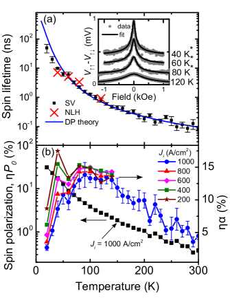
The IDSD measurement results are fit to the numerical solution of Eq. 5, with the spin lifetime and the dimensionless spin injection efficiency as fitting parameters. The fits to the IDSD results are shown as solid lines in Fig. 6, and the temperature dependence of the fitting parameters and are shown in Figs. 8(a) and (b). The product of the detection efficiency and the spin polarization below the injector is also shown in Fig. 8(b).
III.4 Hanle fitting
At low temperatures, at which the NLH measurement could be performed, the spin lifetime obtained from fits of the IDSD measurement could be compared to the spin lifetime measured by Hanle precession experiments. To fit NLH field sweeps the data were fit to the Green’s function solution of Eq. 5 in one dimension, which gives
| (8) |
where 0.62 MHz/Oe is the gyromagnetic ratio in GaAs. Eq. 8 is identical to solving Eq. 5 in one dimension with an added precession term from an external transverse magnetic field , and . The simplification to one dimension is appropriate at low temperatures, because the spin diffusion length is larger than the channel depth of 2.5 m.
III.5 Spin lifetime calculation
In order to compare the measured temperature dependence of the spin lifetime with DP theory, we used the method of Lau, Olesberg, and Flatté (2001, 2004) to calculate the spin relaxation rate for the doping concentration n cm-3. The spin relaxation rate, , can be expressed as
| (9) |
where is the effective-mass approximation density-of-states in the GaAs, is the Fermi-Dirac distribution function, is the component in the multipole expansion of the momentum scattering time, and is the component of the energy-dependent effective SOI magnetic field. The cubic symmetry of the Dresselhaus interaction in bulk GaAs Dresselhaus (1955) results in for all . Eq. 9 is a generalization of the original DP expression D’yakonov and Perel’ (1971); Pikus and Titkov (1984), where the integral over energy in Eq. 9 properly weights the spin relaxation rate to account for an arbitrary degree of degeneracy as well as energy-dependent momentum scattering mechanisms.
In n-GaAs, the dominant scattering mechanism changes from ionized-impurity (II) scattering at low temperatures to optical-phonon (OP) scattering at high temperatures Fletcher and Butcher (1972), as demonstrated by the non-monotonic temperature-dependence of the mobility shown in Fig. 3(a). To determine the momentum scattering time, the experimental mobility is fit to the form
| (10) |
which combines the II and OP scattering rates via Matthiessen’s rule. In Eq. 10, A and B are fitting parameters for the II mechanism and C is a fitting parameter for the OP mechanism. For II scattering, is the known temperature dependence of the scattering time Brooks (1955) and the fitting parameter is added to account for degeneracy at low temperatures. No universal energy exponent can be assigned to OP scattering over the experimental temperature range, due to the breakdown of the relaxation-time approximation Howarth and Sondheimer (1953); Fletcher and Butcher (1972). We find, however, that approximates the measured high temperature mobility. This is not a rigorous relation for OP scattering, but the purpose of Eq. 10 is to provide a phenomenological scattering rate which decreases with temperature (II scattering) and a scattering rate which increases with temperature (OP scattering). The fit to Eq. 10 is shown along with the measured mobility in Fig. 3(a).
After fitting the temperature dependence of the mobility to extract the contributions due to the II and OP scattering mechanisms, each mechanism is separately fit to the expression
| (11) |
to determine (the momentum relaxation time) for each mechanism, at each temperature. The energy dependence of the scattering time is assumed to be , where and for II and OP scattering, respectively Lau et al. (2004). The relevant multipole component of the scattering time for DP relaxation, , can be determined from by expressing the multipole component of the scattering time using the known form of the scattering cross section
| (12) |
where is the Legendre polynomial of degree . Eq. 12 may be evaluated to relate to (for detailed evaluation of Eq. 12 see Ref. Pikus and Titkov, 1984, resulting in for II scattering, and for OP scattering Pikus and Titkov (1984); Lau et al. (2004)).
After fitting the measured mobility with Eq. 10 and 11, the component of the momentum scattering rate is input to Eq. 9, and the DP spin relaxation rate is evaluated at all temperatures. The SOI strength used to evaluate as a function of carrier energy is taken from the calculation with a full fourteen band basis done by Lau et al. (2001). Their calculations give with 25 eV Å3. The final result for the spin lifetime as a function of temperature from Eq. 9 is shown as the blue solid line in Fig. 8(a).
IV Discussion
As shown in Fig. 6, the spin diffusion length falls from approximately 7 m at 20 K to 1 m at room temperature. Injector-detector separations less than approximately 1.0 m are therefore ideal to detect NLSV signals in n-GaAs at room temperature. We emphasize that a two-dimensional model of spin diffusion is needed to fit the separation dependence of when the spin diffusion length is smaller than the channel depth of 2.5 m. Fits using the 1D solution of Eq. 5 underestimate the spin lifetime and spin diffusion length when the channel thickness is greater than a spin diffusion length, because the spin accumulation in two dimensions decays faster than away from the injector.
As can be seen in Fig. 8(a), the temperature dependence of the spin lifetime agrees well with the DP prediction, calculated from Eq. 9, over the entire temperature range. varies from 4916 ns at 20 K to 8610 ps at 300 K. The relatively large uncertainty in the 20 K spin lifetime value results from a lack of data for injector-detector separations larger than the spin diffusion length at low temperature. Separations larger than 10 m would be required to constrain the fit adequately. At low temperatures (40-120 K) we have also measured by the NLH measurement. The spin lifetimes obtained with NLH measurements are also shown on Fig. 8(a), with the NLH field sweeps and fits to Eq. 8 shown in the inset. The values from NLH measurements are in good agreement with the IDSD values above 60 K. At the lowest temperatures (20-40 K), the pulsed NLH measurement technique may not be sufficient to completely remove the effects of DNP. A combined model of the electron-nuclear spin system is needed to adequately model the NLH measurement in the regime where DNP is significant, as is done in Refs. Salis et al. (2009); Chan et al. (2009); Harmon et al. (2015).
We now comment on the magnitude of in the biased-detector SV measurement. Combining Eq. 1 and Eq. 7 allows one to determine the spin accumulation given , the SV signal size. The only unknown is , the detection efficiency. In our devices, we have demonstrated that is a strong function of detector bias, which complicates the interpretation. Because of the detector bias dependence of implied by the data shown in Fig. 5, we also cannot assume , as the injector contact is biased with a large current, while the detector bias is varied. Based on these considerations, the spin polarization of the channel and the injection efficiency may only be quantitatively evaluated up to a factor of (i.e. and , respectively), where is the detection efficiency at the detector bias voltage at which the measurement was performed and is the spin polarization below the injector. These quantities are shown in Fig. 8(b). Although the overall scale for cannot be determined in this experiment, it is believed to be 50% based on spin-LED measurements on similar Fe/GaAs Schottky interfaces Adelmann et al. (2005).
At the lowest temperatures, we measure values of 1 mV with a forward bias applied to a detector contact. This implies that the spin-resolved electrochemical potential splitting at the injector is comparable to the Fermi energy in the GaAs channel, which is 5 meV with respect to the conduction band minimum. As the maximum possible value of is unity, we emphasize that the ordinate scales shown in Fig. 8(b) are therefore minimum values for and . At 20 K, we measure %. Thus, the upper limit of 100% polarization in the GaAs puts a lower limit of 0.3 at 20 K. Notably, because the forward bias current (spin extraction) leads to drift enhancement of the spin accumulation buildup at the injector contact, ideal ferromagnetic contacts ( 1) are not necessary to achieve channel spin polarizations approaching 100% Petukhov et al. (2007); Yu and Flatté (2002).
In Fig. 8(b), a downturn in the injection-detection efficiency product is observed at temperatures below 100 K. To address this observation, we have measured for different injector current biases. The results of this measurement are shown in Fig. 8(b), where it is apparent that is a function of the injector current bias at low temperatures. At temperatures above 150 K, where the spin accumulation is small with respect to the carrier density, becomes independent of injector current bias.
To understand the injector bias current dependence of , we first discuss the influence of an electric field on the spin accumulation. Electric fields at the injector necessarily accompany the bias current. In addition to the drift effects, discussed above, large electric fields in n-GaAs are known to enhance the spin relaxation rate. In n-GaAs, at low temperatures (T 30 K) the itinerant electron temperature can deviate significantly from the lattice temperature due to the dominance of elastic scattering mechanisms, which hinder electron-lattice equilibration Oliver (1962). This electron heating is present above electric fields 10 V/cm, and leads to donor impact ionization, which prevents the electron temperature from cooling below the donor binding energy (6 meV for Si in GaAs Yu and Cardona (1996)). At low temperatures, electric field dependence of the spin lifetime has been widely reported Kato et al. (2004); Beck et al. (2005); Furis et al. (2006). At the lowest temperatures in our experiment (20, 30 K), the suppression of the spin lifetime due to the applied electric field may contribute to the downturn in we observe. However, the injector bias dependence of is observed clearly up to 100 K in Fig. 8(b). At 100 K, all donors are thermally ionized and inelastic electron-phonon relaxation mechanisms are sufficient to prevent any electron-lattice temperature difference. Thus, we believe that electric field suppression of the spin lifetime is not the origin of the injector bias dependence of .
We believe that the downturn in at low temperatures is more likely to be a consequence of the large spin polarization of the channel and consequent breakdown of the ordinary drift-diffusion model. In the presence of a spin accumulation comparable to the carrier density, Eq. 5 must be modified to prevent the spin polarization from achieving non-physical values 100%. Physically, the model parameters themselves become functions of the spin polarization, and the assumption of linear response breaks down Qi et al. (2006). To be specific, it becomes necessary to specify the diffusion constants and spin relaxation rates separately for minority and majority spin carriers, i.e. and , where and are the equilibrium spin relaxation rate and diffusion constant, respectively Vera-Marun et al. (2011). We note that for the DP spin relaxation mechanism () in n-GaAs where II scattering is dominant () the spin relaxation rate is a strong function of carrier energy . The diffusion constant also increases with increasing carrier energy via the Einstein relation (Eq. 6). The mechanisms described above may provide feedback to limit the spin polarization in the large spin polarization regime via more efficient spin diffusion and spin relaxation processes compared to the small spin polarization linear-response limit. If this were the case, then the injector current polarization required to achieve a given spin accumulation would be larger than that calculated under the assumption of linear response.
V Conclusions
In conclusion, we have explored several aspects of spin transport in epitaxial FM/n-GaAs spin valves over a wide range of temperature and bias conditions. Because these devices are based on Schottky tunnel barriers, both the injection and detection efficiencies depend on the bias. We have exploited this property to enhance the sensitivity to spin accumulation by applying a bias current to the detector in the nonlocal configuration. Although the mechanism for the enhancement is not well-understood (except for the role of drift), this approach enables detection of spin accumulation up to room temperature. At injector current densities of A/cm2 nonlocal voltages of order 1 mV are detected at low temperature, which fall to 40 V at room temperature. This approach has enabled measurements of the spin relaxation rate and diffusion length over the entire temperature range, and good agreement is obtained with a model based on the Dyakonov-Perel spin relaxation mechanism. At the lowest temperatures, however, the standard drift-diffusion model appears to break down because of the large spin accumulation, which is comparable to the carrier density. At high temperatures, the devices are limited by the rapidly increasing spin relaxation rate, although the injected current polarization also decreases by a factor of three between 20 K and room temperature.
The devices discussed in this paper are based on Heusler alloys, which are predicted to have a high spin polarization and grow epitaxially on GaAs (001). There is sufficient uncertainty in the derived values of the detection efficiency and injected current polarization that it is not possible to make a statement about the polarization of the Co2FeSi injector beyond the lower bound (30%) set by the size of the nonlocal voltage at the lowest temperature. As suggested by the bias dependence, there is likely a significant contribution to the tunnelling current from interface states, a property that is shared by the epitaxial Fe/GaAs system Chantis et al. (2007). Although these important details still need to be resolved, this work demonstrates that epitaxial FM/III-V heterostructures can be used to probe spin transport at room temperature.
VI Acknowledgments
This work was supported by the National Science Foundation (NSF) under DMR-1104951, C-SPIN, one of the six centers of STARnet, a SRC program sponsored by MARCO and DARPA, the Materials Research Science and Engineering Centers (MRSEC) program of the NSF under DMR 08-19885, and the NSF NNCI program.
References
- Lou et al. (2007) X. Lou, C. Adelmann, S. A. Crooker, E. S. Garlid, J. Zhang, K. S. M. Reddy, S. D. Flexner, C. J. Palmstrøm, and P. A. Crowell, Nat. Phys. 3, 197 (2007).
- Ciorga et al. (2009) M. Ciorga, A. Einwanger, U. Wurstbauer, D. Schuh, W. Wegscheider, and D. Weiss, Phys. Rev. B 79, 165321 (2009).
- Salis et al. (2010) G. Salis, A. Fuhrer, R. R. Schlittler, L. Gross, and S. F. Alvarado, Phys. Rev. B 81, 23 (2010).
- Saito et al. (2013) T. Saito, N. Tezuka, M. Matsuura, and S. Sugimoto, Appl. Phys. Express 6, 103006 (2013).
- Appelbaum et al. (2007) I. Appelbaum, B. Huang, and D. J. Monsma, Nature 447, 295 (2007).
- Tombros et al. (2007) N. Tombros, C. Jozsa, M. Popinciuc, H. T. Jonkman, and B. J. van Wees, Nature 448, 571 (2007).
- Han et al. (2010) W. Han, K. Pi, K. M. McCreary, Y. Li, J. J. I. Wong, A. G. Swartz, and R. K. Kawakami, Phys. Rev. Lett. 105, 167202 (2010).
- Lou et al. (2006) X. Lou, C. Adelmann, M. Furis, S. A. Crooker, C. J. Palmstrøm, and P. A. Crowell, Phys. Rev. Lett. 96, 176603 (2006).
- Kato et al. (2004) Y. K. Kato, R. C. Myers, A. C. Gossard, and D. D. Awschalom, Science 306, 1910 (2004).
- Werake et al. (2011) L. K. Werake, B. A. Ruzicka, and H. Zhao, Phys. Rev. Lett. 106, 107205 (2011).
- Garlid et al. (2010) E. S. Garlid, Q. O. Hu, M. K. Chan, C. J. Palmstrøm, and P. A. Crowell, Phys. Rev. Lett. 105, 156602 (2010).
- Chan et al. (2009) M. K. Chan, Q. O. Hu, J. Zhang, T. Kondo, C. J. Palmstrøm, and P. A. Crowell, Phys. Rev. B 80, 161206 (2009).
- Awo-Affouda et al. (2009) C. Awo-Affouda, O. M. J. van’t Erve, G. Kioseoglou, A. T. Hanbicki, M. Holub, C. H. Li, and B. T. Jonker, Appl. Phys. Lett. 94, 102511 (2009).
- Salis et al. (2009) G. Salis, A. Fuhrer, and S. F. Alvarado, Phys. Rev. B 80, 115332 (2009).
- Dresselhaus (1955) G. Dresselhaus, Phys. Rev. 100, 580 (1955).
- Datta and Das (1990) S. Datta and B. Das, Appl. Phys. Lett. 56, 665 (1990).
- D’yakonov and Perel’ (1971) M. I. D’yakonov and V. I. Perel’, Sov. Phys. JETP 33, 1053 (1971).
- Dzhioev et al. (2002) R. I. Dzhioev, K. V. Kavokin, V. L. Korenev, M. V. Lazarev, B. Y. Meltser, M. N. Stepanova, B. P. Zakharchenya, D. Gammon, and D. S. Katzer, Phys. Rev. B 66, 245204 (2002).
- Pikus and Titkov (1984) G. E. Pikus and A. N. Titkov, in Optical Orientation, edited by F. Meier and B. P. Zakharchenya (North-Holland, Amsterdam, 1984) Chap. 3.
- Kikkawa and Awschalom (1998) J. M. Kikkawa and D. D. Awschalom, Phys. Rev. Lett. 80, 4313 (1998).
- Rashba (2000) E. I. Rashba, Phys. Rev. B 62, R16267 (2000).
- Fert and Jaffrès (2001) A. Fert and H. Jaffrès, Phys. Rev. B 64, 184420 (2001).
- Hanbicki et al. (2001) A. T. Hanbicki, B. T. Jonker, G. Itskos, G. Kioseoglou, and A. Petrou, Appl. Phys. Lett. 80, 1240 (2001).
- Hashimoto et al. (2005) M. Hashimoto, J. Herfort, H.-P. Schönherr, and K. H. Ploog, Appl. Phys. Lett. 87, 102506 (2005).
- Hirohata et al. (2005) A. Hirohata, H. Kurebayashi, S. Okamura, M. Kikuchi, T. Masaki, T. Nozaki, N. Tezuka, and K. Inomata, J. Appl. Phys. 97, 103714 (2005).
- Liu et al. (2014) C. Liu, Y. Boyko, C. C. Geppert, K. D. Christie, G. Stecklein, S. J. Patel, C. J. Palmstrøm, and P. A. Crowell, Appl. Phys. Lett. 105, 212401 (2014).
- Liu et al. (2016) C. Liu, S. J. Patel, T. A. Peterson, C. C. Geppert, K. D. Christie, C. J. Palmstrøm, and P. A. Crowell, Nat. Commun. 7, 10296 (2016).
- Yu and Cardona (1996) P. Y. Yu and M. Cardona, Fundamentals of Semiconductors (Springer-Verlag, Berlin; Heidelberg; New York, 1996).
- Benzaquen et al. (1986) M. Benzaquen, D. Walsh, and K. Mazuruk, Phys. Rev. B 34, 8 (1986).
- Lewis and Sondheimer (1955) B. F. Lewis and E. H. Sondheimer, Proc. R. Soc. London. Ser. A 227, 241 (1955).
- Hanbicki et al. (2003) A. T. Hanbicki, O. M. J. van ’t Erve, R. Magno, G. Kioseoglou, C. H. Li, B. T. Jonker, G. Itskos, R. Mallory, M. Yasar, and A. Petrou, Appl. Phys. Lett. 82, 4092 (2003).
- Cowley and Sze (1965) A. M. Cowley and S. M. Sze, J. Appl. Phys. 36, 3212 (1965).
- Stratton (1969) R. Stratton, in Tunneling Phenomena in Solids, edited by E. Burstein and S. Lundqvist (Plenum Press, New York, 1969) Chap. 8.
- Brinkman et al. (1970) W. F. Brinkman, R. C. Dynes, and J. M. Rowell, J. Appl. Phys. 41, 1915 (1970).
- Johnson and Silsbee (1985) M. Johnson and R. H. Silsbee, Phys. Rev. Lett. 55, 1790 (1985).
- Crooker et al. (2009) S. A. Crooker, E. S. Garlid, A. N. Chantis, D. L. Smith, K. S. M. Reddy, Q. O. Hu, T. Kondo, C. J. Palmstrøm, and P. A. Crowell, Phys. Rev. B 80, 041305 (2009).
- Bruski et al. (2013) P. Bruski, Y. Manzke, R. Farshchi, O. Brandt, J. Herfort, and M. Ramsteiner, Appl. Phys. Lett. 103, 052406 (2013).
- Song and Dery (2010) Y. Song and H. Dery, Phys. Rev. B 81, 045321 (2010).
- Jedema et al. (2002) F. J. Jedema, H. B. Heersche, A. T. Filip, J. J. A. Baselmans, and B. J. van Wees, Nature 416, 713 (2002).
- Yu and Flatté (2002) Z. G. Yu and M. E. Flatté, Phys. Rev. B 66, 201202 (2002).
- Tahara et al. (2016) T. Tahara, Y. Ando, M. Kameno, H. Koike, K. Tanaka, S. Miwa, Y. Suzuki, T. Sasaki, T. Oikawa, and M. Shiraishi, Phys. Rev. B 93, 214406 (2016).
- Chantis and Smith (2008) A. N. Chantis and D. L. Smith, Phys. Rev. B 78 (2008).
- Hu et al. (2011) Q. O. Hu, E. S. Garlid, P. A. Crowell, and C. J. Palmstrøm, Phys. Rev. B 84, 085306 (2011).
- Dery and Sham (2007) H. Dery and L. J. Sham, Phys. Rev. Lett. 98, 046602 (2007).
- Pu et al. (2013) Y. Pu, J. Beardsley, P. M. Odenthal, A. G. Swartz, R. K. Kawakami, P. C. Hammel, E. Johnston-Halperin, J. Sinova, and J. P. Pelz, Appl. Phys. Lett. 103, 012402 (2013).
- Shiogai et al. (2014) J. Shiogai, M. Ciorga, M. Utz, D. Schuh, M. Kohda, D. Bougeard, T. Nojima, J. Nitta, and D. Weiss, Phys. Rev. B 89, 081307 (2014).
- Jansen et al. (2015) R. Jansen, A. Spiesser, H. Saito, and S. Yuasa, Phys. Rev. B 92, 075304 (2015).
- Tran et al. (2009) M. Tran, H. Jaffrès, C. Deranlot, J.-M. George, A. Fert, A. Miard, and A. Lemaître, Phys. Rev. Lett. 102, 036601 (2009).
- Txoperena et al. (2014) O. Txoperena, Y. Song, L. Qing, M. Gobbi, L. E. Hueso, H. Dery, and F. Casanova, Phys. Rev. Lett. 113, 146601 (2014).
- Jansen et al. (2012) R. Jansen, A. M. Deac, H. Saito, and S. Yuasa, Phys. Rev. B 85, 134420 (2012).
- Wurmehl et al. (2005) S. Wurmehl, G. H. Fecher, H. C. Kandpal, V. Ksenofontov, C. Felser, H.-J. Lin, and J. Morais, Phys. Rev. B 72, 184434 (2005).
- Balke et al. (2006) B. Balke, G. H. Fecher, H. C. Kandpal, C. Felser, K. Kobayashi, E. Ikenaga, J.-J. Kim, and S. Ueda, Phys. Rev. B 74, 104405 (2006).
- Picozzi and Freeman (2007) S. Picozzi and A. J. Freeman, J. Phys. Condens. Matter 19, 315215 (2007).
- Chantis et al. (2007) A. N. Chantis, K. D. Belashchenko, D. L. Smith, E. Y. Tsymbal, M. van Schilfgaarde, and R. C. Albers, Phys. Rev. Lett. 99, 1 (2007).
- Christie (2014) K. D. Christie, Non-equilibrium spin accumulation in Co2FexMn1-xSi/n-GaAs heterostructures, Ph.D. thesis, University of Minnesota (2014).
- Lau et al. (2001) W. H. Lau, J. T. Olesberg, and M. E. Flatté, Phys. Rev. B 64, 161301 (2001).
- Lau et al. (2004) W. H. Lau, J. T. Olesberg, and M. E. Flatté, (2004), arXiv:0406201 [cond-mat] .
- Fletcher and Butcher (1972) K. Fletcher and P. N. Butcher, J. Phys. C Solid State Phys. 5, 212 (1972).
- Brooks (1955) H. Brooks, in Adv. Electron. Electron Phys., Vol. 7 (Elsevier, 1955) pp. 85–182.
- Howarth and Sondheimer (1953) D. J. Howarth and E. H. Sondheimer, Proc. R. Soc. London. Ser. A , 53 (1953).
- Harmon et al. (2015) N. J. Harmon, T. A. Peterson, C. C. Geppert, S. J. Patel, C. J. Palmstrøm, P. A. Crowell, and M. E. Flatté, Phys. Rev. B 92, 140201 (2015).
- Adelmann et al. (2005) C. Adelmann, X. Lou, J. Strand, C. J. Palmstrøm, and P. A. Crowell, Phys. Rev. B 71, 121301 (2005).
- Petukhov et al. (2007) A. G. Petukhov, J. Niggemann, V. N. Smelyanskiy, and V. V. Osipov, J. Phys. Condens. Matter 19, 315205 (2007).
- Oliver (1962) D. J. Oliver, Phys. Rev. 127, 1045 (1962).
- Beck et al. (2005) M. Beck, C. Metzner, S. Malzer, and G. H. Döhler, Europhys. Lett. 75, 597 (2005).
- Furis et al. (2006) M. Furis, D. L. Smith, J. L. Reno, and S. A. Crooker, Appl. Phys. Lett. 89, 99 (2006).
- Qi et al. (2006) Y. Qi, Z.-G. Yu, and M. E. Flatté, Phys. Rev. Lett. 96, 026602 (2006).
- Vera-Marun et al. (2011) I. J. Vera-Marun, V. Ranjan, and B. J. van Wees, Nat. Phys. 8, 313 (2011).