Plasmon properties and hybridization effects in Silicene
Abstract
The plasmonic character of monolayer silicene is investigated by time-dependent density functional theory in the random phase approximation. Both the intrinsic (undoped) and several extrinsic (carrier doped or gated) conditions are explored by simulating injection of a probe particle (i.e., an electron or a photon) of energy below 20 eV and in-plane momentum smaller than 1.1 Å−1. The energy-loss function of the system is analyzed, with particular reference to its induced charge-density fluctuations, i.e., plasmon resonances and corresponding dispersions, occurring in the investigated energy-momentum region. At energies larger than eV, two intrinsic interband modes are detected and characterized. The first one is a hybridized -like plasmon, which is assisted by competing one-electron processes involving sp2 and sp3 states, and depends on the slightest changes in specific geometric parameters, such as nearest-neighbor atomic distance and buckling constant. The second one is a more conventional - plasmon, which is more intense than the -like plasmon and more affected by one-electron processes involving the bands with respect to the analogous collective oscillation in monolayer graphene. At energies below eV, two extrinsic intraband modes are predicted to occur, which are generated by distinct types of Dirac electrons (associated with different Fermi velocities at the so-called Dirac points). The most intense of them is a two-dimensional plasmon, having an energy-momentum dispersion that resembles that of a two-dimensional electron gas. The other is an acoustic plasmon that occurs for specific momentum directions and competes with the two-dimensional plasmon at mid-infrared energies. The strong anisotropic character of this mode cannot be explained in terms of the widely used Dirac-cone approximation. As in mono-, bi-, and few-layer graphene, the extrinsic oscillations of silicene are highly sensitive to the concentration of injected or ejected charge carriers. More importantly, the two-dimensional and acoustic plasmons appear to be a signature of the honeycomb lattice, independently of the chemistry of the group-IV elements and the details of the unit-cell geometry.
pacs:
73.20.Mf,73.22.Lp,73.22.PrI Introduction
Atomically thin materials, organized in hexagonal honeycomb like geometry, have been through intense scrutiny due to their exceptional electronic properties, the most intriguing of which is, perhaps, the strong coupling between their quantized charge-density fluctuations, i.e., plasmon modes, and light or other charged particles lin2008operation ; ju2011graphene ; bao2012graphene ; sensale2012broadband ; garcia2014graphene . Control and manipulation of the plasmon properties of these two-dimensional systems, including graphene and beyond, are expected to guide the design of next-generation nanophotonic and nanoelectronic devices, with the enhanced capability to operate from terahertz (THz) to infrared (IR) frequencies. Indeed, plasmon-like modes appear as the “true” low-energy excitations of low-dimensional system haldane_1 ; haldane_2 , while charged and spinful modes are realized as coherent states, with their own peculiar dynamics giula_1 ; giula_2 , both in normal, and in superconducting phases moscio ; giuso_1 ; giuso_2 ; 1367-2630-12-2-025022 . Fundamental research and technological applications have been historically focused on monolayer graphene (MG) GeimNovGraphene2007 ; neto2009electronic , whose extrinsic plasmons exhibit much stronger confinement, larger tunability and lower losses compared to gold and silver nanoparticles christensen2011graphene . Recent studies have thoroughly characterized the plasmon dispersions in MG grigorenko2012graphene ; pisarra2014acoustic ; liou2015pi ; woessner2015highly ; 0022-3727-48-46-465104 ; sindona2016plasmon and some other graphene-related materials, such as bilayer graphene (BLG) FeiBLG2015 ; pisarra2016dielectric and graphene nanoribbons (GNRs) arranged in regular planar arrays, which, unlike MG, offer geometrically controllable band gaps fei2015edge ; vacacela2016gnr ; vacacelaBJNANO2017 . Further advances are expected from the analysis of nanocarbon-metal interfaces together with associated application developments in biological sensing, optical signal processing and quantum information technology AnkerNat2008 ; bao2012graphene ; PhysRevA.92.053812 ; TsargorodskaNL2016 ; acssensors5b00280 ; Genslein2016 .
Nonetheless, the incompatibility of carbon-based materials with current silicon-based electronics makes the former unsuitable for immediate use, for which reason, other candidates among the group-IV elements, e.g., Silicon and Germanium in honeycomb lattice, have been explored houssa2011electronic ; vogt2012silicene ; drummond2012electrically ; kara2012review ; o2012stable ; cai2013stability ; zhao2016rise ; kaloni2016current that, similarly to MG, have, in their free-standing forms, linear dispersing valence () and conduction () bands, crossing at the inequivalent K (and K′) points cahangirov2009two ; liu2011quantum , where charge-carries behave as massless Dirac fermions.
In particular, silicene has been recognized to have four principal advantages with respect to MG: (i) compatibility with current electronics; (ii) large spin-orbit induced band gap of - meV liu2011quantum ; PhysRevB.84.195430 , with respect to the meV value predicted for MG PhysRevB.75.041401 , which has been confirmed by an experimental realization of the quantum spin Hall effect PhysRevLett.112.106802 ; (iii) tunable band gap in the presence of a perpendicular electric field ni2011tunable ; PhysRevB.89.195410 ; PhysRevB.89.201411 ; PhysRevB.90.035142 ; drummond2012electrically , with band gap values of several meV that increase with increasing the field strength, or by hydrogenation Osborn2011101 ; Lu2009153 ; Shyam2014 and fluorination Ding2012 ; and (iv) synthesis on various substrates with different electronic properties zhao2016rise . This and other beyond-graphene systems are expected to be good competitors with graphene-related materials, sharing with the latter many of the superior features of MG, plus enhanced controllable electronic properties for specific applications. A further support in this direction has been the fabrication of a silicene-based field-effect-transistor tao2015silicene .
From the structural point of view, atomic resolved scanning tunneling microscopy (STM) experiments, combined with density-functional calculations vogt2012silicene ; lin2012structure ; feng2012evidence ; Shyam2014 , have demonstrated that silicene is characterized by a buckled honeycomb lattice where the sp2 hybridized orbitals get slightly dehybridized into sp3 like orbitals causing a weakening of the bonds. This mixed sp2-sp3 hybridization yields a nearest-neighbor Si-Si distance of - Å and a low buckling of - Å.
On the practical side, silicene has been successfully grown on transition metals, such as Ag(001), Ag(110), Ag(111) kara2012review ; zhao2016rise ; kaloni2016current , Ir(111) meng2013buckled , metal dichalcogenides, like MoS2 gao2014tunable ; Qian1256815 , and ceramic materials, e.g., ZrB2(0001) fleurence2012experimental . Combined experimental and theoretical studies have demonstrated that the Dirac cone disappears in silicene grown on Ag substrates, due to strong hybridization between Si and Ag orbitals lin2013substrate ; guo2013absence ; cahangirov2013electronic ; PhysRevB.89.201416 . Further theoretical scrutiny has also predicted silicene to be energetically stable (with unperturbed Dirac cones) on h-BN, H-passivated C-SiC(0001), Si-SiC(0001), Cl-passivated Si(111), CaF2, AlAs(111), AlP(111), GaAs(111), GaP(111), ZnSe(111), and ZnS(111) kaloni2016current ; guo2013absence ; kaloni2013quasi ; liu2013silicene ; kokott2014nonmetallic ; noguchi2015direct . Semiconducting substrates with large band gaps like h-BN turn out to be excellent candidates to adsorb pristine silicene, simply because no substrate states appear close to the Fermi level and, accordingly, the interaction silicene-substrate cannot perturb the Dirac-cone structure.
Although the structural properties of pristine silicene are well established, a comprehensive approach and description of its plasmon properties at low and high energies, from the IR to ultraviolet (UV) range, has not been presented so far. A few theoretical studies mohan2013first ; das2015optical ; matthes2013universal ; matthes2014optical , based on the analysis of the electron energy-loss function and absorption spectrum, have reported the existence of two interband plasmons in intrinsic silicene, occurring at energies larger than eV for vanishingly small momentum transfers. These are counterparts to the well-known and - plasmons found in MG, BLG and graphite eberlein2008plasmon . Otherwise, MG, silicene and germanene have been proved to have the same IR frequency absorbance bechstedt2012infrared , which is a universal feature of the two-dimensional honeycomb lattice and does not depend on the chemistry of the group-IV element, buckling parameter or hybridization state. Furthermore, some noteworthy approaches have investigated the effect of an external, perpendicular electric field PhysRevB.89.195410 ; PhysRevB.89.201411 , plus an additional exchange field PhysRevB.90.035142 , probing the spin-orbit band-structure of silicene, below some tenths of eV around the K and K′ points. In these studies, the use of an effective two-spinor Hamiltonian, with an emergent Dirac-cone structure perturbed by spin-orbit PhysRevLett.95.226801 and external/field terms, has revealed presence and interplay of extrinsic plasmons, at meV energies and far-IR wave lengths, displaying features of different regimes, including those of a topological insulator and a valley-spin polarized metal. In the same energy-momentum region, of key-interest for nanodevice applications, it has been demonstrated that the electron-phonon interaction plays a critical role PhysRevB.88.121403 ; WangJAP2015 , leading the in-plane phonon modes to hybridize with the extrinsic plasmons.
Here, we present a full ab initio approach, based on time-dependent (TD) density functional theory (DFT) within the random phase approximation (RPA), to scrutinize the plasmon properties of pristine and doped silicene in absence of external fields and spin-orbit effects, which makes an excellent approximation for applications in the mid-IR to UV range, with the plasmon-phonon coupling reduced to a minor extent. First, we focus on the intrinsic IR and UV plasmons, whose long-wavelength behavior is in agreement with the absorbance predictions of Refs. matthes2013universal, and matthes2014optical, . In particular, we describe the role played by sp2 and sp3 hybridization in the Landau damping mechanism, which affects the silicene counterpart of the MG plasmon. Next, we discuss the mid-IR to near-IR extrinsic plasmons, highlighting the occurrence of two distinct tunable modes, which may be seen as a universal feature of the gapless band-structure of group IV elements in honeycomb lattice.
Our arguments are organized as follows. In section II, we briefly outline the key concepts of our TDDFT+RPA scheme, suitable for two-dimensional periodic systems. In section III, we analyze the energy-loss spectrum of silicene at high energies (larger than eV), with reference to the coupling of the intrinsic plasmons and single-particle (SP) processes, involving sp2 and sp3 hybridized states. In section IV, we investigate the low-energy end of the energy-loss spectrum (below eV) in the presence of carrier doping, and show the interrelation between two extrinsic intraband modes: one of them is a two-dimensional plasmon, already observed in a variety of graphene-based materials; the other is an acoustic plasmon, direct consequence of the anisotropic band structure of the system around the Dirac points, i.e., the failure of the Dirac-cone approximation. In section V, we draw our conclusions.
II Methods
In this section, we first provide the input parameters of our ground-state density functional calculations of monolayer silicene (Sec. II.1). Then, we highlight the main features of our TDDFT approach, yielding the complex permittivity and loss function of the system under both intrinsic and extrinsic conditions (Sec. II.2). Hartree atomic units are used throughout, unless otherwise stated. All calculations were performed on a high performance computing cluster GALILEO-SCAI , using up to 512 CPUs on 32 nodes with 3840 Gb memory.
II.1 DFT calculation
The equilibrium electronic properties of silicene were determined by DFT in the local density approximation (LDA) perdew1981self , with the Kohn-Sham (KS) electron wave functions expanded in the plane-wave (PW) basis gonze2009abinit . The latter is represented by the space functions
| (1) |
where is a wave vector in the first Brillouin zone (BZ), a reciprocal-lattice vector, and the unit-cell volume associated to the real-space lattice [Fig. 1(a) and 1(b)]. The number of PWs was limited by the energy cut off Hartrees. Norm conserving pseudopotentials of the Troullier-Martins type were adopted to eliminate the core electrons troullier1991efficient . The three-dimensional periodicity inherent in our PW-DFT approach was generated by replicating the silicene planes with a minimum separation of Å.
Geometry optimization and ground state calculations were carried out on the irreducible part of the first BZ [ triangle in Fig. 1(b)], using a -centered and unshifted Monkhorst-Pack (MP) grid of points monkhorst1976special . The optimized lattice constant and buckling parameter were found to be Å and Å, respectively [Fig. 1(a)]. Slightly larger lattice-constant values available from the literature liu2011quantum ; liu2013silicene ; BalendhranSmall2014 ; Shyam2014 were also tested, while keeping the buckling parameter fixed to its optimized value (see Appendix A).
As for the LDA electronic structure, the KS energies and wave functions
| (2) |
were computed for bands, with the sum being limited by the energy cut off condition set forth above to include coefficients per wave function.
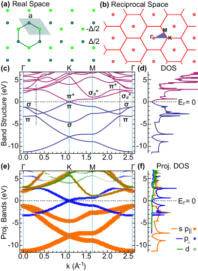
A simple visual perspective of the band energies [Fig. 1(c)] shows that silicene presents a Dirac-cone structure at the points, within eV around the Fermi energy . Looking at the density of states (DOS) as function of the band energies [Fig. 1(d)], we notice that the two peaks closest to correspond to and flat band dispersions at the point [Fig. 1(c)]. Other two peculiar DOS-peak structures, appearing at - eV above and below , are direct consequence of the mixed sp2-sp3 hybridization and buckled conformation of silicene. A more-detailed insight into these hybridization mechanisms is offered by the orbital projected band structure and DOS of Fig. 1(e) and 1(f), respectively, where we have separated the contribution of and states, forming like bonds, from states, involved in bonds, and states of the unit-cell Si atoms. The valence bands have well-defined and characters, with sharp avoided-crossing features in correspondence of the DOS peaks at - eV below . The conduction states above the Dirac point are also of the form, yielding an antibonding band responsible for the DOS peak at eV above cahangirov2009two . Another conduction band denoted lies close to the band and produces a DOS peak at eV above . It has a dominant -character contaminated by states. Other conduction bands are strongly influenced by , , and higher principal quantum numbers, as it can be deduced by comparing the full DOS and its projected , and components at energies larger than eV above .
These characteristics (not found in MG PhysRevB.89.165430 ) play an important role in the plasmonic properties of silicene at probing energies larger than eV, as we will see in Sec. III.
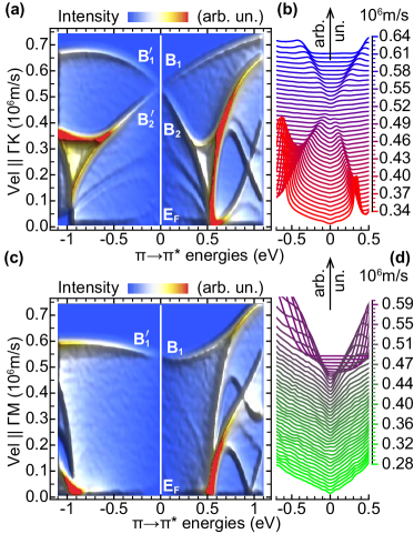
As for the Dirac point features of the - electrons, an average Fermi-velocity value m/s can be extracted from the band data, which is roughly of that derived from local density calculations in MG, and reflects a relatively reduced mobility of the massless Dirac fermions of Silicene. A more detailed analysis is made possible by inspection of the partial DOS as function of the - energies and group velocities parallel to K [Figs. 2(a) and 2(b)] and M [Fig. 2(c) and 2(d)]. Along K, the DOS is peaked at two distinct Fermi-velocity values, corresponding to the B, B branches below and the B1, B2 branches above in Fig. 2(a). On the other hand, along M, the DOS is peaked around one single Fermi-velocity value, associated to the B branch below and B1 branch above in Fig. 2(c).
Like in MG pisarra2014acoustic ; sindona2016plasmon , this anisotropic behavior is outside the Dirac-cone approximation, and yields markedly different extrinsic plasmon responses at probing energies smaller than eV.
II.2 TDDFT+RPA approach
Plasmons in solid state materials are typically triggered by electron-beam radiation or photo-currents below a few eV, and charged ions with incident kinetic energy of the order of 0.1-1 keVRiccardi2003339 ; PhysRevB.72.165419 ; Sindona20072805 ; RiccardiJPhys2010 ; Cupolillo20101029 ; RiccardiAPL2012 ; Ligato201440 ; Pisarra2014796 . In the present context, we consider introducing an electron or a photon, with incident momentum and frequency , which weakly perturbs the KS electrons of silicene. The unperturbed density-density response function of the system to the test particle is provided by the Adler-Wiser formula kubo1957statistical ; adler1962quantum ; wiser1963dielectric . The latter is generally represented in the reciprocal space as follows
| (3) |
Here, the factor of accounts for the spin degeneracy, labels the Fermi-Dirac distribution,
| (4) |
are density-density correlation matrix elements, and yields a positive broadening (chosen to the value of eV).
The interacting density-density response function stems from the central equation of TDDFT petersilka1996excitation ; onida2002electronic
| (5) |
where represent the Fourier coefficients of an effective electron-electron interaction. In the RPA, these terms are approximated to the bare Coulomb potential:
| (6) |
where a purely 3D periodic system is taken into account. The drawback of this approach is the non-negligible interaction between the periodic replicas, no matter how large their relative distance is. To cancel out this unphysical phenomenon, basically due to the long-range character of the Coulomb potential, we replace Eq. (6) by the truncated Fourier integral over the out-of-plane axis ():
| (7) |
where and denote the in-plane and out-of-plane components of . Eq. (7), tending to Eq. (6) for , has been proved to establish a proper two-dimensional cut off despoja2012ab ; despoja2013two ; novko2015changing ; pisarra2016dielectric , eliminating the interaction between charge densities located at the different slabs.
Once the interacting matrix elements in Eq. (5) have been set by Eq. (7), the inverse dielectric matrix is obtained as
| (8) |
Collective excitations (plasmons) are established by the zeros in the real part of the macroscopic dielectric function (permittivity) , whose imaginary part gives the optical absorption spectrum.
The plasmon structure is provided by the energy-loss function, being proportional to the imaginary part of the inverse permittivity:
| (9) |
Nonlocal field effects are included in Eq. (9) through the off-diagonal elements of kramberger2008linear . As in MG and BLG, we verified that vectors of the form , sorted in length order from smallest to largest, lead to well-converged results.
In what follows we discuss the dielectric and energy-loss properties of silicene, as obtained from the outlined TDDFT+RPA scheme at room temperature and under several intrinsic or extrinsic conditions.
III Intrinsic silicene
The ground-state electron density for the optimized lattice constant Å and buckling parameter Å (Sec. II.1) was used–in a non self consistent run–to improve the resolution on the KS eigensystem . The latter was recalculated on an MP mesh of points, including up to bands. This result was plugged in the TDDFT+RPA machinery, summarized by Eqs. (3)-(9), to have an accurate representation of the electronic excitations and energy loss properties up to eV. Similar calculations were run for the lattice-constant values and Å, as reported in Appendix A.
The energy-loss spectrum of undoped (intrinsic) silicene, with the LDA optimized geometry, is reported in Fig. 3 for a broad range of frequencies, ranging from the lower THz to the UV, and incident momenta along K and M. Two plasmon structures can be clearly distinguished, i.e., a like plasmon and a - plasmon that are peaked respectively at eV and eV, in correspondence with the lowest sampled values, being smaller than Å-1. The outlined interband modes are counterparts to the well-known and - plasmons of MG, BLG, fewlayer graphene (i.e., five to ten stacked MG sheets) and graphite eberlein2008plasmon ; despoja2012ab ; despoja2013two ; pisarra2014acoustic ; pisarra2016dielectric ; sindona2016plasmon , sharing with the former a squareroot behavior of the energy-momentum dispersions in the optical region. Nevertheless, the reduced width of the () and () bands [Fig. 1(b)] and the peculiar DOS features [Fig. 1(c)], which characterize silicene with respect to MG, cause a red-shift and a different relative weight of the intrinsic plasmon peaks.

Indeed the and - structures of MG have similar peak intensities eberlein2008plasmon , whereas the - peak of silicene is generally larger (by a factor of 3 at Å-1) than the like peak. This fact can be ascribed to the weakening of the bonds in silicene due to the mixed - hybridization discussed in Sec. II.1. Another distinctive aspect of the intrinsic response of silicene is the double (quasilinear) dispersion of the like plasmon in the energy-momentum region eV and Å-1, along M [Fig. 3(c) and 3(d)]. In this region, the collective oscillation is associated to SP excitations between high DOS points connecting the and or bands [Fig. 1(c)].
A more detailed view on the like plasmon is offered by Fig. 4, where we see how the very close (or overlapping) energy levels in the and bands [Fig. 1(c)] generate distinct plasmon features at high-DOS points [Fig. 1(d)]. For small incident momenta around the point ( Å-1) and energies below eV, the large DOS peak hides the contribution [Fig. 1(d) and 1(f)], and a single plasmon character dominates along both K and M. As increases above Å-1 and gets larger than eV, the component increases becoming of the same order as the component [Fig. 1(d) and 1(f)]. This increase is associated to a larger splitting between the antibonding bands, which leads to a well-resolved two-peak structure in the energy-loss spectra. The latter presents markedly distinct features along K and M, being a signature of the deeply anisotropic character of the dielectric response of the system. In either cases, the like plasmon is indeed a hybridized plasmon where the role of - and - components, i.e., the relative spectral weight of the associated SP processes, is modulated by the excited electronic structure. In addition, slight changes in the lattice constant cause some distortions of the like plasmon peaks without altering the peak ratio of the - and - parts (Appendix. A).
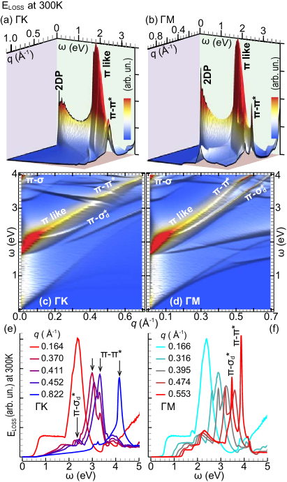
Besides the like and - plasmons, Fig. 4 also shows a nonnegligible intraband plasmon, peaked at energies below eV, which is generated by a conduction electron concentration of cm-2 at room temperature. This value is larger than the one found in MG, because of the smaller Fermi-velocity values that characterize silicene, in spite of its larger unit-cell area, which correspond to a lower slope in the vanishing DOS at the K points (Figs. 1 and 2). The intraband feature is barely visible in Figs. 3 and 4, where it is hidden by the onset of the like structure. However, it can be detected at the lowest ’s in Figs. 5 and Figs. 12 (of Appendix A), where an extra peak below eV is clearly spotted in both and . Hence, intraband plasmons are also possible in the intrinsic limit when finite temperature is considered.
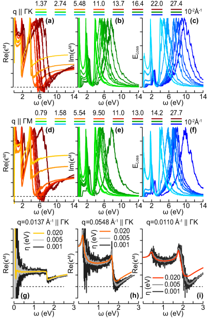
From a closer analysis of , we realize that only the - peak is a well-defined plasmon in a specific region of the energy-momentum domain, with Å-1 and eV, where it corresponds to a zero in at a frequency where is small. All other like and - structures can still be treated as collective excitations, superimposed to SP processes between high-DOS points, whose average lifetime broadening ( eV in Eq. (3)) induces a large Landau damping.
A parallel situation has been observed in MG despoja2013two ; pisarra2014acoustic ; novko2015changing ; pisarra2016dielectric . Indeed, as we let the lifetime broadening parameter tend artificially to zero, the condition for occurrence of a collective oscillation becomes more and more likely to be satisfied. In support of this argument, Figs. 5(g)-5(i) display for , and eV. The intraband and -like plasmon structures are evidently related to quasi-zeros in . Interestingly enough, the complex permittivity and energy-loss function display a nearly isotropic behavior for small values of the transferred momentum, below Å-1, while as gets larger than Å-1 the dielectric response of the system acquires a tensor character. Similar trends have been reported for MG kramberger2008linear ; pisarra2014acoustic and BLG pisarra2016dielectric . As for the absorption spectrum, reflects the main features of the energy-loss function with two or three optical peaks (including the intraband mode at low ) being clearly spotted. The interband peak positions at energies larger than eV are in agreement with previous absorbance calculations matthes2013universal ; matthes2014optical . We should point out that our predictions are based on the two-dimensional cut off procedure outlined in the previous section, while the use of the bare Coulomb interaction would lead to an erroneous positioning of the optical plasmon-peaks (see Appendix B).
IV Extrinsic silicene
We now move to the loss properties of extrinsic silicene with LDA-optimized geometry. In Appendix A, we will discuss how the effect of stretching the lattice constant (from to and Å) does not alter the extrinsic plasmon features. In what follows, we specifically consider four different charge-carrier concentrations, inducing negative and positive Fermi energy shifts , in the range of to eV, relative to the Dirac-point energy. To achieve these extrinsic conditions, we adjusted the occupation factors and in Eq. (3) by shifting the Fermi-energy values by and eV, respectively. A summary of the sampled doping levels–and corresponding conduction-electron or valence-hole densities–is given in Table 1. The like and - plasmons of the previous section were found to be rather insensitive to the simulated extrinsic conditions, as already indicated by several studies on graphene-related systems pisarra2014acoustic ; pisarra2016dielectric ; vacacela2016gnr ; vacacelaBJNANO2017 . Then, we present a zoomed view of the energy-momentum region eV, Å-1, which was computed with the TDDFT+RPA method illustrated in Sec. II.2, using an equilibrium electronic structure represented on an MP grid of points and bands.
| (eV) | (el per uc) | ||
|---|---|---|---|
| -0.4 | -0.0510 | -4.039 | -4.098 |
| -0.2 | -0.0126 | -1.000 | -1.055 |
| 0.0 | - | - | 0.029 |
| 0.2 | 0.0135 | 1.071 | 1.136 |
| 0.4 | 0.0597 | 4.727 | 4.863 |
The energy-loss spectra for eV and eV are shown as density plots in Figs. 6 and 7, respectively. The most striking feature here is the appearance of two distinct plasmon resonances, which are nearly absent in intrinsic silicene at room temperature [Fig. 4(a) and 4(c)].
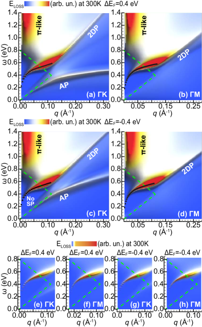
The most intense peak is associated to a two-dimensional plasmon, denoted 2DP, which is clearly manifested along both K and M, and exhibits a dispersion at optical wave lengths, as the conventional plasmon of a two-dimensional electron gas. This mode has been predicted and analyzed in a number of theoretical studies on extrinsic MG, ranging from two-band models in the Dirac cone approximation Sarma.PhysRevB.75.205418 to TDDFT approaches pisarra2014acoustic ; sindona2016plasmon ; despoja2013two , and it is at the heart of technological applications in graphene plasmonics ju2011graphene ; bao2012graphene ; garcia2014graphene .
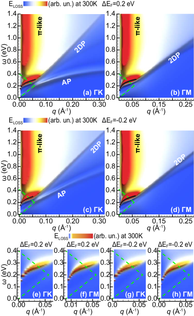
Despite the difference in intensity, a second plasmon of acoustic nature, denoted AP, is clearly visible for momentum transfers along K, being generated by the two type of Dirac electrons responsible for the different Fermi-velocity values along [Fig. 2(a) and 2(b)]. The 2DP corresponds to the two types of electrons oscillating in-phase with one another, and the AP mode corresponds to electrons oscillating out-of-phase. This mode has been originally identified in MG pisarra2014acoustic ; sindona2016plasmon and offers a linear energy-dispersion in the low- limit.
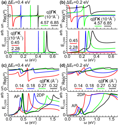
A signature of the asymmetric dielectric response of the material is provided by the observation that the 2DP mode is present along both K and M, whereas the AP mode is present only along K. This means that the widely used Dirac cone approximation is capable of reproducing only the 2DP features. By comparing Figs. 6 and 7, we see that interplay between the 2DP and the AP is strongly sensitive to the extrinsic conditions, including the doping sign, being associated to different charge-carrier densities (Table I). More importantly, there is a region in the energy-momentum domain, corresponding to Å-1, eV, where the AP mode is competitive with the 2DP. Although many recent calculations have reported the existence of two extrinsic plasmons in graphene-related materials pisarra2016dielectric ; Low.PhysRevLett.112.116801 , the peculiarity of the AP mode in silicene and MG pisarra2014acoustic ; sindona2016plasmon is that it occurs in a single, virtually gapless band. Our study suggests that the occurrence of such a mode is another universal characteristic of the honeycomb lattice (in addition to the above mentioned infrared absorbance). It is worth mentioning that the 2DP and the like structure tend to get closer to each other, as the doping decreases. This is why at room temperature and zero doping the onset of like mode mostly hides the 2DP contribution [as already pointed out in Sec. III, with reference to Figs. 4 and 5].
Also interesting to notice is the opening of a gap in the SP excitation spectrum for low and , along both K and M. Such a gap is in close agreement with the triangular region predicted by two-band models in the Dirac cone approximation Sarma.PhysRevB.75.205418 . The latter is delimited the by dashed green lines in Figs. 6 and 7, which correspond to and (with being the average Fermi-velocity introduced in Sec. II.1).
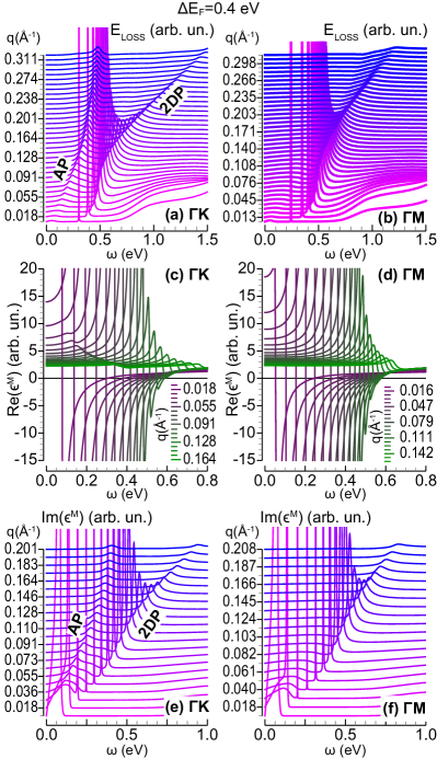
The 2DP falls onto the no-SP excitation region at the lowest ’s, where it appears as a sharp peak not affected by Landau damping, as displayed in Figs. 6(e)-6(h), 7(e)-7(h), 8(a) and 8(b). Accordingly, the real permittivity has well defined zeros in this region [reported as black dots in Figs. 6(a)-6(d) and 7(a)-7(d)]. For points outside the no-SP excitation region, the 2DP gets more and more damped, with the condition being violated at large values, as shown in Fig. 8(c) and 8(d), where the competition mechanism between the 2DP and AP modes is emphasized. This explains why the intrinsic response of Silicene does not offer well-defined plasmon excitations, with the area of the no-SP-excitation region being virtually zero. As a further evidence in support of this argument, in Fig. 9 we show a complete analysis of the macroscopic dielectric function and the two-plasmon structure for eV. Indeed, Figs. 9(c), 9(d) prove that the 2DP is a genuine collective oscillation in the no-SP-excitation region. On the other hand the AP mode lies outside this region, and the corresponding plasmon oscillation is always damped in the Landau sense.
V Conclusions
We have presented a full TDDFT+RPA analysis of the dielectric properties and plasmon dispersion of intrinsic and extrinsic silicene in freestanding form, in absence of external fields and spin-orbit coupling, suitable for energies above eV and incident momenta larger than Å-1. The energy-loss spectra of intrinsic silicene have singled out two interband plasmon structures, lying at energies above 1.5 eV, which resembles the and - modes of MG. The low- features of the plasmon peaks have been found in agreement with previous absorbance calculations bechstedt2012infrared . A more careful analysis has revealed that the like plasmon of silicene is assisted by SP processes between hybridized sp2 and sp3 states, connecting the band to the and like bands, which generates a double energy-momentum dispersion, best resolved for momentum transfers along . Similar characteristics are expected to occur also in other buckled two-dimensional materials in honeycomb geometry, such as germanene.
At lower energies (below eV), the energy-loss spectra of extrinsic silicene show two distinct oscillations, whose relative strength can be modulated by the doping concentration of injected or ejected electrons. Similarly to MG, silicene presents a two-dimensional plasmon, which shares many common features with the plasmon mode of a two-dimensional electron gas, plus an acoustic mode, being observable only along specific directions of the incident momentum. Unlike the spin-polarized and valley modes found at meV energies and far-IR momentum transfers PhysRevB.89.195410 ; PhysRevB.89.201411 ; PhysRevB.90.035142 , being related to the opening of a band gap, these two modes are generated in a gapless band-structure by two different types of charge carriers, i.e., Dirac electrons moving with distinct Fermi velocities.
Our findings suggest that the 2DP and AP modes exist in other two-dimensional materials in honeycomb lattice, such as germanene, making this features independent on the chemistry of the group-IV element, buckling parameter, or hybridization state. More importantly, they support the argument that silicene-based nanomaterials are excellent options for the design of next-generation nanodevices, in competition with graphene-based nanomaterials.
Acknowledgements C.V.G. acknowledges the financial support of “Secretaria Nacional de Educación Superior, Ciencia, Tecnología e Innovación” (SENESCYT-ECUADOR). A. S. acknowledges the computing facilities provided by the CINECA Consortium GALILEO-SCAI , within the INF16_npqcd project under the CINECA-INFN agreement.
Appendix A Influence of the unit-cell extension on the plasmon structure
In this first Appendix, we report on how the loss properties of silicene are affected by geometry, specifically focusing on the intrinsic like and extrinsic plasmon features, analyzed in Sec. III and IV, respectively. To this end, we applied the TDDFT+RPA scheme on three different Si-Si bond lengths (yielding the lattice constant values 3.82, 3.86, 3.89 Å that have been quoted in the literature BalendhranSmall2014 . The buckling parameter has been fixed to its LDA-optimized value in all cases (0.45 Å).
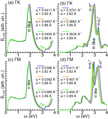
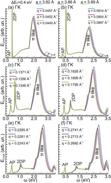
The calculated loss function is shown in Fig. 10 for intrinsic silicene and Fig. 11 for extrinsic silicene. The only sensible effect is a red-shift of the like plasmon peaks with the increase of . In particular, at long wavelengths, peak variations of 3.8 (along for Å-1) and 1.3 (along for Å-1) are recorded in response to a change in lattice constant of 1.8. The same change yields a peak variation of 4 at small wavelengths along both and for - Å-1. The extrinsic plasmon structure appears to be independent on lattice-constant variations considered here.
Appendix B Role of the two-dimensional cut off on the Coulomb interaction
To complete our study, we focus on the long wavelength limit (Å−1) and mid infrared to near ultraviolet frequency range ( eV) of the plasmon spectra of undoped silicene, and consider some previous theoretical results in comparison with the findings presented in the main text.
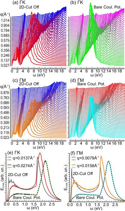
Mohan and coworkers mohan2013first have reported two-plasmon features, with the -plasmon lying at 2.16 eV and the --plasmon being peaked at 7.6 eV. The same peaks have been predicted to be around 2 eV and 9 eV, respectively, by Das et al das2015optical . To verify these results, we have solved the Dysonlike equation for the full susceptibility (Eq. (5)) with the bare Coulomb potential coefficients (Eq. (6)). The resulting loss function presents a narrow -plasmon peak at 2 eV and a broad --plasmon peak at 7 eV along both K and M, at the lowest sampled values [Fig. 12(b) and 12(d)]. On the other hand, with the two-dimensional cut off procedure outlined in the main text the very same two plasmons appear red-shifted [Fig. 12(a) and 12(c)], in agreement with the calculations by Matthes and coworkers matthes2013universal ; matthes2014optical . The disagreement between the two approaches is particularly strong at the lowest sampled points, as attested by the plots of Fig. 12(e) and 12(f). This result adds up to a number of previous studies despoja2012ab ; despoja2013two ; novko2015changing ; pisarra2016dielectric where it has been pointed out that the correct way to investigate and describe the dielectric properties of a two-dimensional system is provided by Eqs.(3)-(9). The calculations of Fig. 12 also demonstrate that applying a two-dimensional cut off on the Coulomb potential becomes unnecessary for values of the momentum transfer larger than Å-1, which is not surprising because the larger -components of the Coulomb potential do not contribute to coupling of the repeated slab.
References
- (1) Y.-M. Lin, K. A. Jenkins, A. Valdes-Garcia, J. P. Small, D. B. Farmer, and P. Avouris, Operation of graphene transistors at gigahertz frequencies, Nano Lett. 9, 422 (2008).
- (2) L. Ju, B. Geng, J. Horng, C. Girit, M. Martin, Z. Hao, H. A. Bechtel, X. Liang, A. Zettl, Y. R. Shen, et al., Graphene plasmonics for tunable terahertz metamaterials, Nat. Nanotechnol. 6, 630 (2011).
- (3) Q. Bao and K. P. Loh, Graphene photonics, plasmonics, and broadband optoelectronic devices, ACS Nano 6, 3677 (2012).
- (4) B. Sensale-Rodriguez, R. Yan, M. M. Kelly, T. Fang, K. Tahy, W. S. Hwang, D. Jena, L. Liu, and H. G. Xing, Broadband graphene terahertz modulators enabled by intraband transitions, Nat. Commun. 3, 780 (2012).
- (5) F. J. Garcia de Abajo, Graphene plasmonics: challenges and opportunities, ACS Photonics 1, 135 (2014).
- (6) F. D. M. Haldane, Exact Jastrow-Gutzwiller resonating-valence-bond ground state of the spin-1/2 antiferromagnetic Heisenberg chain with 1/ exchange, Phys. Rev. Lett. 60, 635 (1988).
- (7) F. D. M. Haldane, “Spinon gas” description of the Heisenberg chain with inverse-square exchange: Exact spectrum and thermodynamics, Phys. Rev. Lett. 66, 1529 (1991).
- (8) B. A. Bernevig, D. Giuliano, and R. B. Laughlin, Spinon Attraction in Spin- Antiferromagnetic Chains, Phys. Rev. Lett. 86, 3392 (2001).
- (9) B. A. Bernevig, D. Giuliano, and R. B. Laughlin, Spinon-Holon Attraction in the Supersymmetric Model with 1/ Interaction, Phys. Rev. Lett. 87, 177206 (2001).
- (10) J. E. Mooij and G. Schön, Propagating plasma mode in thin superconducting filaments, Phys. Rev. Lett. 55, 114 (1985).
- (11) D. Giuliano and P. Sodano, Boundary field theory approach to the renormalization of SQUID devices, Nucl. Phys. B 770, 332 (2007).
- (12) D. Giuliano and P. Sodano, Competing boundary interactions in a Josephson junction network with an impurity, Nucl. Phys. B 837, 153 (2010).
- (13) D. Giuliano, A. Sindona, G. Falcone, F. Plastina, and L. Amico, Entanglement in a spin system with inverse square statistical interaction, New J. Phys. 12, 025022 (2010).
- (14) A. K. Geim and K. S. Novoselov, The rise of graphene, Nat. Mater. 6, 183 (2007).
- (15) A. H. Castro Neto, F. Guinea, N. M. R. Peres, K. S. Novoselov, and A. K. Geim, The electronic properties of graphene, Rev. Mod. Phys. 81, 109 (2009).
- (16) J. Christensen, A. Manjavacas, S. Thongrattanasiri, F. H. L. Koppens, and F. J. García de Abajo, Graphene plasmon waveguiding and hybridization in individual and paired nanoribbons, ACS Nano 6, 431 (2011).
- (17) A. N. Grigorenko, M. Polini, and K. S. Novoselov, Graphene Plasmonics, Nat. Photon. 6, 749 (2012).
- (18) M. Pisarra, A. Sindona, P. Riccardi, V. M. Silkin, and J. M. Pitarke, Acoustic plasmons in extrinsic free-standing graphene, New J. Phys. 16, 083003 (2014).
- (19) S. C. Liou, C.-S. Shie, C. H. Chen, R. Breitwieser, W. W. Pai, G. Y. Guo, and M.-W. Chu, -plasmon dispersion in free-standing graphene by momentum-resolved electron energy-loss spectroscopy, Phys. Rev. B 91, 045418 (2015).
- (20) A. Woessner, M. B. Lundeberg, Y. Gao, A. Principi, P. Alonso-González, M. Carrega, K. Watanabe, T. Taniguchi, G. Vignale, M. Polini, et al., Highly confined low-loss plasmons in graphene–boron nitride heterostructures, Nat. Mater. 14, 421 (2015).
- (21) D. Mencarelli, S. Bellucci, A. Sindona, and L. Pierantoni, Spatial dispersion effects upon local excitation of extrinsic plasmons in a graphene micro-disk, J. Phys. D: Appl. Phys. 48, 465104 (2015).
- (22) A. Sindona, M. Pisarra, D. Mencarelli, L. Pierantoni, and S. Bellucci, Plasmon Modes in Extrinsic Graphene: Ab initio Simulations vs Semi-classical Models, in “Fundamental and Applied Nano-Electromagnetics”, chap. 7, pp. 125-144, Springer, 2016.
- (23) Z. Fei, E. G. Iwinski, G. X. Ni, L. M. Zhang, W. Bao, A. S. Rodin, Y. Lee, M. Wagner, M. K. Liu, S. Dai, M. D. Goldflam, M. Thiemens, F. Keilmann, C. N. Lau, A. H. Castro-Neto, M. M. Fogler, and D. N. Basov, Tunneling Plasmonics in Bilayer Graphene, Nano Lett. 15, 4973 (2015).
- (24) M. Pisarra, A. Sindona, M. Gravina, V. M. Silkin, and J. M. Pitarke, Dielectric screening and plasmon resonances in bilayer graphene, Phys. Rev. B 93, 035440 (2016).
- (25) Z. Fei, M. Goldflam, J.-S. Wu, S. Dai, M. Wagner, A. McLeod, M. Liu, K. Post, S. Zhu, G. Janssen, et al., Edge and surface plasmons in graphene nanoribbons, Nano Lett. 15, 8271 (2015).
- (26) C. Vacacela Gomez, M. Pisarra, M. Gravina, J. M. Pitarke, and A. Sindona, Plasmon Modes of Graphene Nanoribbons with Periodic Planar Arrangements, Phys. Rev. Lett. 117, 116801 (2016).
- (27) C. Vacacela Gomez, M. Pisarra, M. Gravina, , and A. Sindona, Tunable plasmons in regular planar arrays of graphene nanoribbons with armchair and zigzag-shaped edges, Beilstein J. Nanotechnol. 8, 172 (2017).
- (28) J. N. Anker, W. P. Hall, O. Lyandres, N. C. Shah, J. Zhao, and R. P. Van Duyne, Biosensing with plasmonic nanosensors, Nat. Mater. 7, 442 (2008).
- (29) W. Fan, B. J. Lawrie, and R. C. Pooser, Quantum plasmonic sensing, Phys. Rev. A 92, 053812 (2015).
- (30) A. Tsargorodska, M. L. Cartron, C. Vasilev, G. Kodali, O. A. Mass, J. J. Baumberg, P. L. Dutton, C. N. Hunter, P. Törmä, and G. J. Leggett, Strong Coupling of Localized Surface Plasmons to Excitons in Light-Harvesting Complexes, Nano Lett. 16, 6850 (2016).
- (31) M. Couture, K. K. Ray, H.-P. Poirier-Richard, A. Crofton, and J.-F. Masson, 96-Well Plasmonic Sensing with Nanohole Arrays, ACS Sensors 1, 287 (2016).
- (32) C. Genslein, P. Hausler, E.-M. Kirchner, R. Bierl, A. J. Baeumner, and T. Hirsch, Graphene-enhanced plasmonic nanohole arrays for environmental sensing in aqueous samples, Beilstein J. Nanotechnol. 7, 1564 (2016).
- (33) M. Houssa, E. Scalise, K. Sankaran, G. Pourtois, V. Afanas’Ev, and A. Stesmans, Electronic properties of hydrogenated silicene and germanene, Appl. Phys. Lett. 98, 223107 (2011).
- (34) P. Vogt, P. De Padova, C. Quaresima, J. Avila, E. Frantzeskakis, M. C. Asensio, A. Resta, B. Ealet, and G. Le Lay, Silicene: Compelling Experimental Evidence for Graphenelike Two-Dimensional Silicon, Phys. Rev. Lett. 108, 155501 (2012).
- (35) N. D. Drummond, V. Zólyomi, and V. I. Fal’ko, Electrically tunable band gap in silicene, Phys. Rev. B 85, 075423 (2012).
- (36) A. Kara, H. Enriquez, A. P. Seitsonen, L. L. Y. Voon, S. Vizzini, B. Aufray, and H. Oughaddou, A review on silicene- new candidate for electronics, Surf. Sci. Rep. 67, 1 (2012).
- (37) A. O’Hare, F. V. Kusmartsev, and K. I. Kugel, A Stable “Flat” Form of Two-Dimensional Crystals: Could Graphene, Silicene, Germanene Be Minigap Semiconductors?, Nano Lett. 12, 1045 (2012).
- (38) Y. Cai, C.-P. Chuu, C. M. Wei, and M. Y. Chou, Stability and electronic properties of two-dimensional silicene and germanene on graphene, Phys. Rev. B 88, 245408 (2013).
- (39) J. Zhao, H. Liu, Z. Yu, R. Quhe, S. Zhou, Y. Wang, C. C. Liu, H. Zhong, N. Han, J. Lu, et al., Rise of silicene: A competitive 2D material, Prog. Mater. Sci. 83, 24 (2016).
- (40) T. P. Kaloni, G. Schreckenbach, M. S. Freund, and U. Schwingenschlögl, Current developments in silicene and germanene, Phys. Status Solidi Rapid Res. Lett. 10, 133 (2016).
- (41) S. Cahangirov, M. Topsakal, E. Aktürk, H. Şahin, and S. Ciraci, Two- and One-Dimensional Honeycomb Structures of Silicon and Germanium, Phys. Rev. Lett. 102, 236804 (2009).
- (42) C.-C. Liu, W. Feng, and Y. Yao, Quantum Spin Hall Effect in Silicene and Two-Dimensional Germanium, Phys. Rev. Lett. 107, 076802 (2011).
- (43) C.-C. Liu, H. Jiang, and Y. Yao, Low-energy effective Hamiltonian involving spin-orbit coupling in silicene and two-dimensional germanium and tin, Phys. Rev. B 84, 195430 (2011).
- (44) Y. Yao, F. Ye, X.-L. Qi, S.-C. Zhang, and Z. Fang, Spin-orbit gap of graphene: First-principles calculations, Phys. Rev. B 75, 041401 (2007).
- (45) H. Pan, Z. Li, C.-C. Liu, G. Zhu, Z. Qiao, and Y. Yao, Valley-Polarized Quantum Anomalous Hall Effect in Silicene, Phys. Rev. Lett. 112, 106802 (2014).
- (46) Z. Ni, Q. Liu, K. Tang, J. Zheng, J. Zhou, R. Qin, Z. Gao, D. Yu, and J. Lu, Tunable bandgap in silicene and germanene, Nano Lett. 12, 113 (2011).
- (47) C. J. Tabert and E. J. Nicol, Dynamical polarization function, plasmons, and screening in silicene and other buckled honeycomb lattices, Phys. Rev. B 89, 195410 (2014).
- (48) H.-R. Chang, J. Zhou, H. Zhang, and Y. Yao, Probing the topological phase transition via density oscillations in silicene and germanene, Phys. Rev. B 89, 201411 (2014).
- (49) B. Van Duppen, P. Vasilopoulos, and F. M. Peeters, Spin and valley polarization of plasmons in silicene due to external fields, Phys. Rev. B 90, 035142 (2014).
- (50) T. H. Osborn, A. A. Farajian, O. V. Pupysheva, R. S. Aga, and L. L. Y. Voon, Ab initio simulations of silicene hydrogenation, Chem. Phys. Lett. 511, 101 (2011).
- (51) A. Lu, X. Yang, and R. Zhang, Electronic and optical properties of single-layered silicon sheets, Solid State Commun. 149, 153 (2009).
- (52) S. Trivedi, A. Srivastava, and R. Kurchania, Silicene and Germanene: A First Principle Study of Electronic Structure and Effect of Hydrogenation-Passivation, J. Comput. Theor. Nanosci. 11, 781 (2014).
- (53) Y. Ding and Y. Wang, Electronic structures of silicene fluoride and hydride, Appl. Phys. Lett. 100, 083102 (2012).
- (54) L. Tao, E. Cinquanta, D. Chiappe, C. Grazianetti, M. Fanciulli, M. Dubey, A. Molle, and D. Akinwande, Silicene field-effect transistors operating at room temperature, Nat. Nanotechnol. 10, 227 (2015).
- (55) C.-L. Lin, R. Arafune, K. Kawahara, N. Tsukahara, E. Minamitani, Y. Kim, N. Takagi, and M. Kawai, Structure of silicene grown on Ag(111), Appl. Phys. Express 5, 045802 (2012).
- (56) B. Feng, Z. Ding, S. Meng, Y. Yao, X. He, P. Cheng, L. Chen, and K. Wu, Evidence of silicene in honeycomb structures of silicon on Ag(111), Nano Lett. 12, 3507 (2012).
- (57) L. Meng, Y. Wang, L. Zhang, S. Du, R. Wu, L. Li, Y. Zhang, G. Li, H. Zhou, W. A. Hofer, and H.-J. Gao, Buckled Silicene Formation on Ir(111), Nano Lett. 13, 685 (2013).
- (58) N. Gao, J. C. Li, and Q. Jiang, Tunable band gaps in silicene-MoS2 heterobilayers, Phys. Chem. Chem. Phys. 16, 11673 (2014).
- (59) X. Qian, J. Liu, L. Fu, and J. Li, Quantum spin Hall effect in two-dimensional transition metal dichalcogenides, Science 346, 1344 (2014).
- (60) A. Fleurence, R. Friedlein, T. Ozaki, H. Kawai, Y. Wang, and Y. Yamada-Takamura, Experimental Evidence for Epitaxial Silicene on Diboride Thin Films, Phys. Rev. Lett. 108, 245501 (2012).
- (61) C.-L. Lin, R. Arafune, K. Kawahara, M. Kanno, N. Tsukahara, E. Minamitani, Y. Kim, M. Kawai, and N. Takagi, Substrate-Induced Symmetry Breaking in Silicene, Phys. Rev. Lett. 110, 076801 (2013).
- (62) Z.-X. Guo, S. Furuya, J.-i. Iwata, and A. Oshiyama, Absence and presence of Dirac electrons in silicene on substrates, Phys. Rev. B 87, 235435 (2013).
- (63) S. Cahangirov, M. Audiffred, P. Tang, A. Iacomino, W. Duan, G. Merino, and A. Rubio, Electronic structure of silicene on Ag(111): Strong hybridization effects, Phys. Rev. B 88, 035432 (2013).
- (64) S. K. Mahatha, P. Moras, V. Bellini, P. M. Sheverdyaeva, C. Struzzi, L. Petaccia, and C. Carbone, Silicene on Ag(111): A honeycomb lattice without Dirac bands, Phys. Rev. B 89, 201416 (2014).
- (65) T. P. Kaloni, M. Tahir, and U. Schwingenschlögl, Quasi free-standing silicene in a superlattice with hexagonal boron nitride, Sci. Rep. 3, 3192 (2013).
- (66) H. Liu, J. Gao, and J. Zhao, Silicene on substrates: a way to preserve or tune its electronic properties, J. Phys. Chem. C 117, 10353 (2013).
- (67) S. Kokott, P. Pflugradt, L. Matthes, and F. Bechstedt, Nonmetallic substrates for growth of silicene: an ab initio prediction, J. Phys.: Condens. Matter 26, 185002 (2014).
- (68) E. Noguchi, K. Sugawara, R. Yaokawa, T. Hitosugi, H. Nakano, and T. Takahashi, Direct Observation of Dirac Cone in Multilayer Silicene Intercalation Compound CaSi2, Adv. Mater. 27, 856 (2015).
- (69) B. Mohan, A. Kumar, and P. Ahluwalia, A first principle calculation of electronic and dielectric properties of electrically gated low-buckled mono and bilayer silicene, Physica E 53, 233 (2013).
- (70) R. Das, S. Chowdhury, A. Majumdar, and D. Jana, Optical properties of P and Al doped silicene: a first principles study, RSC Advances 5, 41 (2015).
- (71) L. Matthes, P. Gori, O. Pulci, and F. Bechstedt, Universal infrared absorbance of two-dimensional honeycomb group-IV crystals, Phys. Rev. B 87, 035438 (2013).
- (72) L. Matthes, O. Pulci, and F. Bechstedt, Optical properties of two-dimensional honeycomb crystals graphene, silicene, germanene, and tinene from first principles, New J. Phys. 16, 105007 (2014).
- (73) T. Eberlein, U. Bangert, R. R. Nair, R. Jones, M. Gass, A. L. Bleloch, K. S. Novoselov, A. Geim, and P. R. Briddon, Plasmon spectroscopy of free-standing graphene films, Phys. Rev. B 77, 233406 (2008).
- (74) F. Bechstedt, L. Matthes, P. Gori, and O. Pulci, Infrared absorbance of silicene and germanene, Appl. Phys. Lett. 100, 261906 (2012).
- (75) C. L. Kane and E. J. Mele, Quantum Spin Hall Effect in Graphene, Phys. Rev. Lett. 95, 226801 (2005).
- (76) J.-A. Yan, R. Stein, D. M. Schaefer, X.-Q. Wang, and M. Y. Chou, Electron-phonon coupling in two-dimensional silicene and germanene, Phys. Rev. B 88, 121403 (2013).
- (77) Z. Wang, T. Feng, and X. Ruan, Thermal conductivity and spectral phonon properties of freestanding and supported silicene, J. Appl. Phys. 117, 084317 (2015).
- (78) GALILEO–Tier-1 cluster for industrial and public research, provided by the CINECA Consortium (Italy), within the INF16_npqcd project under the CINECA-INFN agreement.
- (79) J. P. Perdew and A. Zunger, Self-interaction correction to density-functional approximations for many-electron systems, Phys. Rev. B 23, 5048 (1981).
- (80) X. Gonze, B. Amadon, P.-M. Anglade, J.-M. Beuken, F. Bottin, P. Boulanger, F. Bruneval, D. Caliste, R. Caracas, M. Cote, et al., ABINIT: First-principles approach to material and nanosystem properties, Comput. Phys. Commun. 180, 2582 (2009).
- (81) N. Troullier and J. L. Martins, Efficient pseudopotentials for plane-wave calculations, Phys. Rev. B 43, 1993 (1991).
- (82) H. J. Monkhorst and J. D. Pack, Special points for Brillouin-zone integrations, Phys. Rev. B 13, 5188 (1976).
- (83) S. Balendhran, S. Walia, H. Nili, S. Sriram, and M. Bhaskaran, Elemental Analogues of Graphene: Silicene, Germanene, Stanene, and Phosphorene, Small 11, 640 (2015).
- (84) E. Kogan, V. U. Nazarov, V. M. Silkin, and M. Kaveh, Energy bands in graphene: Comparison between the tight-binding model and ab initio calculations, Phys. Rev. B 89, 165430 (2014).
- (85) P. Riccardi, A. Sindona, P. Barone, A. Bonanno, A. Oliva, and R. Baragiola, Bulk and surface plasmon excitation in the interaction of He+ with Mg surfaces, Nucl. Instr. Meth. Phys. Res. B 212, 339 (2003).
- (86) M. Commisso, M. Minniti, A. Sindona, A. Bonanno, A. Oliva, R. A. Baragiola, and P. Riccardi, Kinetic electron excitation in the interaction of slow Kr+ ions with Al surfaces, Phys. Rev. B 72, 165419 (2005).
- (87) A. Sindona, F. Plastina, A. Cupolillo, C. Giallombardo, G. Falcone, and L. Papagno, Many body shake up in X-ray photoemission from bundles of lithium-intercalated single-walled carbon nanotubes, Surf. Sci. 601, 2805 (2007); A. Sindona, M. Pisarra, S. Maletta, M. Commisso, P. Riccardi, A. Bonanno, P. Barone, G. Falcone, Role of Many Body Shake-Up in Core-Valence-Valence Electron Emission from Single Wall Carbon Nanotubes, J. Nanosci. Nanotechnol. 11, 9143 (2011).
- (88) P. Riccardi, M. Pisarra, A. Cupolillo, M. Commisso, A. Sindona, R. A. Baragiola, and C. A. Dukes, Secondary electron emission spectra from clean and cesiated Al surfaces: the role of plasmon decay and data analysis for applications, J. Phys.: Condens. Matter 22, 305004 (2010).
- (89) A. Cupolillo, M. Pisarra, A. Sindona, M. Commisso, and P. Riccardi, Electron excitation in the interaction of slow ions and electrons with metals and monolayer graphite on Ni(111) surfaces, Vacuum 84, 1029 (2010); A. Sindona, P. Riccardi, S. Maletta, M Pisarra, A. Cupolillo, Wave-packet study of hyperthermal alkali ion neutralization at metal surfaces, Vacuum 84, 1038 (2010).
- (90) P. Riccardi, A. Cupolillo, M. Pisarra, A. Sindona, and L. S. Caputi, Primary energy dependence of secondary electron emission from graphene adsorbed on Ni(111), Appl. Phys. Lett. 101 (2012).
- (91) N. Ligato, A. Cupolillo, A. Sindona, P. Riccardi, M. Pisarra, and L. Caputi, A comparative study of the plasmonic properties of graphene on lattice-matched and lattice-mismatched Ni surfaces, Surf. Sci. 626, 40 (2014).
- (92) M. Pisarra, P. Riccardi, A. Sindona, A. Cupolillo, N. Ligato, C. Giallombardo, and L. Caputi, Probing graphene interfaces with secondary electrons, Carbon 77, 796 (2014); A. Sindona, M. Pisarra, P. Riccardi, and G. Falcone, Cluster and Periodic Density Functional Study of Auger Electron Emission from Conducting Carbon Nanotubes, Nanosci. Nanotechnol. Lett. 4, 1050 (2012).
- (93) R. Kubo, Statistical-Mechanical Theory of Irreversible Processes. I. General Theory and Simple Applications to Magnetic and Conduction Problems, J. Phys. Soc. Jpn. 12, 570 (1957).
- (94) S. L. Adler, Quantum theory of the dielectric constant in real solids, Phys. Rev. 126, 413 (1962).
- (95) N. Wiser, Dielectric constant with local field effects included, Phys. Rev. 129, 62 (1963).
- (96) M. Petersilka, U. J. Gossmann, and E. K. U. Gross, Excitation Energies from Time-Dependent Density-Functional Theory, Phys. Rev. Lett. 76, 1212 (1996).
- (97) G. Onida, L. Reining, and A. Rubio, Electronic excitations: density-functional versus many-body Green’s-function approaches, Rev. Mod. Phys. 74, 601 (2002).
- (98) V. Despoja, K. Dekanić, M. Šunjić, and L. Marušić, Ab initio study of energy loss and wake potential in the vicinity of a graphene monolayer, Phys. Rev. B 86, 165419 (2012).
- (99) V. Despoja, D. Novko, K. Dekanić, M. Šunjić, and L. Marušić, Two-dimensional and plasmon spectra in pristine and doped graphene, Phys. Rev. B 87, 075447 (2013).
- (100) D. Novko, V. Despoja, and M. Šunjić, Changing character of electronic transitions in graphene: From single-particle excitations to plasmons, Phys. Rev. B 91, 195407 (2015).
- (101) C. Kramberger, R. Hambach, C. Giorgetti, M. H. Rümmeli, M. Knupfer, J. Fink, B. Büchner, L. Reining, E. Einarsson, S. Maruyama, F. Sottile, K. Hannewald, V. Olevano, A. G. Marinopoulos, and T. Pichler, Linear Plasmon Dispersion in Single-Wall Carbon Nanotubes and the Collective Excitation Spectrum of Graphene, Phys. Rev. Lett. 100, 196803 (2008).
- (102) E. H. Hwang and S. Das Sarma, Dielectric function, screening, and plasmons in two-dimensional graphene, Phys. Rev. B 75, 205418 (2007).
- (103) T. Low, F. Guinea, H. Yan, F. Xia, and P. Avouris, Novel Midinfrared Plasmonic Properties of Bilayer Graphene, Phys. Rev. Lett. 112, 116801 (2014).