Periodic metallic stepped-slits for entire transmission of optical wave and efficient transmission of terahertz wave
Abstract
Metallic structures with periodic array of slits are well-known to lead to extraordinary power transmission, when slits have dimensions much less than the wavelength of incident optical wave. Excellent power transmission originates from surface waves excited by incident transverse magnetic wave. Here we show that metallic structure with array of stepped-slits can transmit power of incident wave into the substrate at desired optical frequency entirely and simultaneously in terahertz frequency band by 70%, for substrate. Transmitted power of the proposed structure is studied both in a closed-form by an analytical model as well as numerically by finite element method. It is found that with the increase of field intensity in the substrate, structure with array of stepped-slits (as opposed to uniform-slits) favorably has no reduction of frequency range at maximum transmitted power.
Index Terms:
stepped-slits, transmitted power, periodic array, optical wave, terahertz wave.I Introduction
Since the pioneering work of Ebbesen et al.[1] on holes, extraordinary power transmission through periodic metallic structures with dimensions much less than the wavelength of incident wave, has attracted growing interests among researchers [2, 3]. This unusual at the same time interesting phenomena, happens due to excited surface waves in subwavelength structure which mitigate its power reflection. Extraordinary power transmission has brought subwavelength structures into practical applications also, in terahertz sources and detectors [4], chemical sensing [5], spectroscopy and imaging techniques [6, 7], ultrafast photodetectors [8], and high efficiency solar cells [9], to name a few. To be more specific on the subject, photoconductive antennas, a class of terahertz sources and detectors, are well-known to suffer from low radiated power [10, 11, 12, 13]. Their performance can be improved by the use of subwavelength structures which was proposed for the first time by Jarrahi and co-workers [14, 15, 16], as a result of two facts. First, the time required for photocarriers (electrons and holes) generated in photoconductive area, to arrive at radiating electrodes decreases. Second, power reflection at optical and terahertz frequencies can be reduced, as will be shown here [17].
In this work we propose and study the use of stepped slits for reduction of power reflection at both optical frequency as well as terahertz frequency band. The contents of this paper are as follows: Section \@slowromancapii@ develops a theoretical model and subsequently obtains a closed-form expression for the power reflected from the structure. Section \@slowromancapiii@ then discusses how to design a structure with maximum power transmission at desired frequencies. Finally, results from theoretical model are compared with finite element method calculations for specific values of dimensions and frequencies.
II Theory
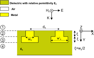
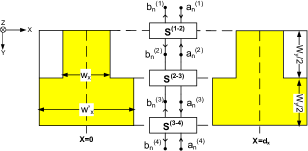
The X-Y cross view of the proposed periodic metallic structure is shown in Fig. 1; all dimensions stay the same through the Z-direction. The structure consists of two nano-scale layered metallic rods with similar height and different widths. The widths of the upper and bottom rods are, respectively, and . These rods are repeated along the X-axis with periodicity . For the sake of generality of the theoretical model proposed in this work for different wavelengths, metallic rods are considered as perfect conductors with infinite conductivity. The X-Y cross section can be seen as of consisting of four different regions, shown by 1 through 4 in Fig. 1. Regions 1 and 4 are infinite uniform mediums, and regions 2 and 3 are periodic regions. Electromagnetic wave incident to the periodic structure can be considered as either transverse electric (TE) with electric field or transverse magnetic (TM) with magnetic field in the Z-direction. In this paper, the TM-polarized incident wave which excites surface wave and subsequently contributes in extraordinary power transmission, is considered for analysis. The theoretical model is built up by expressing electromagnetic fields in both uniform regions 1 and 4 as well as parallel plate waveguide (PPWG) regions 2 (top PPWG) and 3 (bottom PPWG), as Fourier series expansions. Scattering matrices are considered for different interfaces existing in the structure; for the interface between air medium 1 and the top PPWG, for the interface between the top and the bottom PPWGs, and for the interface between the bottom PPWG and the dielectric substrate 4. In order to analyze the performance of the proposed structure on impinging TM-polarized wave, scattering matrices , (i, j)=(1, 2), (2, 3), and (3, 4), are first calculated and then combined based on cascade networks rule as in the followings.
II-A Calculation of Matrix
To obtain the matrix, magnetic fields inside regions 1 and 2, respectively, are expressed as Eqs. (1) and (2) below ([18]):
| (1) |
| (2) |
where , and and are nth-order diffraction coefficients for incident and reflected waves, respectively, in the region i, i=1, 2. Propagation constant, , along Y-axis for nth-order diffraction mode in region i is
| (3) |
for region i=1, and
| (4) |
for region i=2. is the relative permittivity constant of dielectric in regions 2, 3 and 4, and is free-space wavenumber. in Eq. (4) is the initial propagation constant along X-axis. For the special case of normally incident TM-polarized wave, is zero, as will be assumed in this study. It is noted that to propagate nth-order diffraction mode in regions i=1 and 2, its propagation constant along Y-direction must be real. Modes with pure imaginary values of decay rapidly by distance from y=0. Based on Eqs. (3) and (4), at high enough wavelength values (low enough values of ), all values of propagation constant along Y-axis in regions i=1 and 2 are pure imaginary except for fundamental mode, n=0, that is real. In fact, all non-zero orders () of diffraction modes are evanescent in regions 1 and 2. Therefore from here on we will focus on the fundamental mode only. By substituting Eqs. (1) and (2) into the Maxwell’s equation, , tangential electric field components in regions i=1 and 2 are calculated as
| (5) |
| (6) |
In order to obtain coefficient in regions i=1 and 2, continuity equations for tangential electric and magnetic components at the interface of regions 1 and 2 (y=0) are used:
| (7a) | |||
| (7b) | |||
By considering and in the forms of Eqs. (1) and (2), respectively, boundary condition (7a) can be written as
| (8) |
Similarly, boundary condition (7b) can be written as below by expanding the electric field, , according to Eqs. (5) and (6):
| (9) |
Multiplying both sides of Eqs. (8) and (9) by and integrating over a period from to would lead to the following system of linear algebraic equations for coefficients , , and :
| (10) |
| (11) |
As mentioned in the followings of Eq. (4), at high enough wavelength values, and for are pure imaginary; and so, they decay rapidly in Y-direction distance from y=0. Therefore, incident and reflected coefficients, , , , , of guided order diffraction mode m=0 and n=0, are considered in Eqs. (10) and (11) only. By substituting m=0 and n=0, coefficients of zeroth-order diffraction mode are calculated in matrix form as
| (16) |
with
| (17) |
Reflection coefficient at and transmission coefficient at can be obtained from:
| (22) |
where is the transferring matrix:
| (23) |
II-B Calculation of Matrix
In order to calculate the scattering matrix at the interface of regions 2 and 3, , magnetic fields in the upper and lower sides of PPWGs (in the middle of stepped-slit) interface are required. Similar to Fourier series expansion Eq. (2) which was valid for region 2, magnetic field in region 3 can be expanded as
| (24) |
where the minus sign comes to be consistent with the convention of Fig. 2. is the propagation constant along Y-direction for nth-order diffraction mode in region 3 written as
| (25) |
To obtain the x-component of electric field in region 3, , a similar procedure as the one that led to Eq. (6) should be carried out, which will give
| (26) |
Reflection coefficients , i=2, 3, can be calculated from the boundary conditions at the interface of regions 2 and 3; i.e. and should vary continuously across :
| (27a) | |||
| (27b) | |||
By substituting Eqs. (2), (6), (24) and (26) into the Eqs. (27a) and (27b), and multiplying both sides by and subsequently integrating over the slot of bottom PPWG , the following system of algebraic equations will be obtained for reflection and transmission coefficients and for the fundamental mode:
| (32) |
where is
| (33) |
Reflection coefficient and transmission coefficient at respectively and can be obtained from
| (38) |
where the transferring matrix
| (39) |
describes the relation between at and as well as at and .
II-C Calculation of Matrix
The scattering matrix at the interface of regions 3 and 4, can be calculated in a similar fashion as what we did in Section II-A for calculating . Note that here region 4 is the substrate with relative permittivity constant, .
II-D Calculation of Total Scattering Matrix,
The total scattering matrix can be calculated by successive cascade of transferred interface scattering from
| (40) |
where here-defined operator Cas{A, B} operates on two by two matrices A and B as ([19])
| (41) |
Subsequently, the total reflection coefficient at y=0 and total transmission coefficient at can be obtained as
| (46) |
Here, for the sake of brevity, only the expression for is presented
| (47a) | |||
| with | |||
| (47b) | |||
| (47c) | |||
where and are, respectively, the normalized widths of top and bottom metallic rods.
III Results And Discussion
III-A Design Method
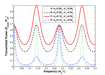
Analytical expression for the reflection coefficient of zeroth-order diffraction mode for the impinging TM-polarized wave on the structure was calculated in the last section as Eq. (47a). The power transmitted into the substrate, depends on the wavelength of the incident wave, periodicity of the structure, width of the top metallic rod, width of the bottom metallic rod, height of stepped-slit, and relative permittivity constant of the dielectric of structure. In this section, the dielectric is assumed to be , with relative permittivity constant 11.7 ([20]) and absorption coefficient 8000 [21]. The ultimate goal of the design is to achieve a structure with maximum transmitted power of incident TM-polarized wave at a specific optical frequency and all the range of terahertz frequency bandwidth, by determining the associated parameters. Fig. 3 shows the transmitted power calculated by our theoretical model with respect to height of the proposed structure (normalized to wavelength) at several widths and of metallic rods; different curves correspond to different values of and . Several resonant guided modes can be observed in the figure. However, first guided mode, at close to zero, is a non-resonant mode. At this mode, the wavelength of the impinging wave is much more than the height of structure, and metallic rods widths have no effect on the power transmitted into the substrate. Maximum transmission power at this mode is
| (48) |
Frequency values of the resonant modes in Fig. 3 agree well with proposed by the reference [22]. However for certain ratios of and (for example shown by red curve) transmitted power with much larger values than those reported in [22] for uniform slit structure, can be obtained at certain frequencies. This is an interesting property of stepped periodic metallic structures, and will be discussed further later. It is also noted that frequency values of resonant guided modes depend on only, whereas transmitted power depends on solely and . Therefore at the first step of design, the height of the structure is determined, based on the optical frequency desired to transmit maximum electromagnetic power. Maximum power transmission is read at from Fig. 3.
Field intensity, I in unit depth of the substrate can be calculated from
| (49) |
where is the power transmitted into the substrate, and is the bottom slit width. According to the above equation I increases with the increase of . Fig. 3 contains for uniform-slit structure, A and B, as well as stepped-slit structures C and D. First comparing two uniform-slit structures A and B, since and at , so . Frequency bandwidth of A though has a smaller value than that of B. Therefore, in metallic arrays of uniform slits, field intensity I and frequency bandwidth have opposite trends of change, such that simultaneous enhancement of both quantities field intensity and bandwidth is impossible, as has been also pointed out by [22]. Second comparing stepped-slit structure D with uniform-slit structure A, at , and , therefore . At the same time, frequency bandwidth of D is larger than that of A. As a result, as opposed to uniform-slits arrays, interestingly metallic arrays with stepped-slits can be utilized for increasing the frequency bandwidth, while preserving field intensity I in the substrate constant.
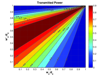
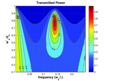
In the second step of design, suitable widths and should be determined. To this end, transmitted power of TM-incident wave has been calculated from Eq. (47a), and is plotted in Fig. 4 as a function of and , for , and absorption coefficient 8000 . The equi-level surfaces are triangles, and the one corresponding to maximum power transmission of 99% is shown by dark red color with the base at . Note that the special case of reduces the stepped slit to uniform slit with maximum power transmission of 70%. Therefore, interestingly, almost entire power transmission is possible for metallic array of stepped slits, which was not the case for uniform slits.
Here we assume . Fig. 5 demonstrates transmitted power of TM-incident wave as a function of and . Power transmission as high as even 99% is possible for certain values of . Moreover, the magnitude of power transmissivity at THz frequency (non-resonant mode) in Fig. 5 is independent of metallic rods widths ( and ) and its value is about 70%; this fact was also observed in Fig. 3 for small values of . According to Fig. 5, at , maximum power transmission of 99% corresponds to .
III-B Results of the Designed Structure
In the previous section, normalized structure parameters were designed to be , , and . For the sake of comparison, the same values for and are adopted here in the analytical and numerical models as those of reference [22]; =1.5 m and =400 nm, leading to =200 nm, =240 nm, and =320 nm. Fig. 6 shows the designed structure as well as its transmitted power calculated both analytically using Eq. (47a) and numerically by the finite element method (FEM) within COMSOL package.
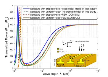
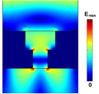
Transmitted power for a uniform-slits array having similar dimensions =400 nm, =200 nm as the stepped-slits array but with =320 nm has been also plotted in Fig. 6 for comparison purpose. Analytical results of Fig. 6 show good agreements with FEM results for both stepped-slits and uniform-slits arrays. The slight difference between resonance wavelength of green and brown curves corresponding to uniform-slits array, can be justified as follows, in contrast to which considered in the proposed theoretical model, the guided mode of PPWGs slightly penetrates into air () and substrate (). This fact can be think of as considering the effective value of in the FEM model to be larger than the value of in the analytical model, i.e. . On the other hand, according to Fig. 3, at first resonance mode . Therefore, , which justifies the difference between analytic and FEM resonance wavelengths of Fig. 6 for uniform-slits arrays. A similar reasoning applies to the difference between resonance wavelength of blue and red curves associated with stepped-slits arrays. As for comparison between performance of stepped- and uniform-slits arrays, maximum transmitted power of stepped-slits array reaches to the impressive value of about 100% at =1.5-1.6 m. For the case of uniform-slits array this value is only 70%. This fact is also confirmed by Fig. 7 which shows that the value of electric field inside the substrate of stepped-slits arrays is larger than that inside uniform-slits arrays. At terahertz frequency band though, both stepped- and uniform-slits arrays have maximum transmitted power of 70%. Therefore, the designed stepped-slits array can transmit entire power of incident wave at optical frequency, while simultaneously transmitting 70% at terahertz frequency band.
IV Conclusion
Periodic metallic structures have been of both research interest and practical implication for power transmission at optical frequencies. Surface waves excited by incident transverse magnetic wave are responsible for power transmission through structure into the substrate. In this paper, metallic structure with periodic array of stepped-slits was suggested. A closed-form expression for the power transmitted through the structure was obtained. The expression takes on structure height, top and bottom slit widths, permittivity constant of dielectric substrate, and frequency as unknown parameters. Conversely, for given optical wavelength corresponding to the entire power transmission, dimensions of the structure can be designed. As an example, for typical optical wavelength of 1.5 m, results show that 70% of incident power is transmitted to substrate in terahertz frequency band, simultaneous to the entire power transmission at the optical frequency of design. As opposed to uniform-slits, with stepped-slits field intensity in the substrate can be increased while preserving frequency range of maximum power transmission constant. All the results were validated numerically by finite element method. For the purpose of increasing efficiency as well as radiated terahertz power, the proposed structure can find applications in the periodic structure of plasmonic photoconductive antennas.
References
- [1] T. W. Ebbesen and H. J. Lezec and H. F. Ghaemi and T. Thio and P. A. Wolff, “Extraordinary optical transmission through sub-wavelength hole arrays,” Nature 391.6668 (1998).
- [2] F. Miyamaru and M. Kamijyo and N. Hanaoka and Mitsuo W. Takeda, “Controlling extraordinary transmission characteristics of metal hole arrays with spoof surface plasmons,” Appl. Phys. Lett., 100, 081112 (2012).
- [3] A. Khavasi and M. Edalatipour and K. Mehrany, “Circuit model for extraordinary transmission through periodic array of subwavelength stepped slits,” IEEE Trans. on Antenna and Propagation, 61, No. 4, 2019-2024 (2013).
- [4] N. Wang and M. R. Hashemi and M. Jarrahi, “Plasmonic photoconductive detectors for enhanced terahertz detection sensitivity,” Opt. Exp., 21, No. 14, 17221-7 (2013).
- [5] J. C. Yang and J. Ji and J. M. Hogle and D. N. Larson, “Metallic nanohole arrays on fluoropolymer substrates as small label-free real-time bioprobes,” Nano Lett., 8 (9), 2718-2724 (2008).
- [6] A. Hartschuh and E. J. Sanchez and X. S. Xie and L. Novotny, “High-resolution near-field raman microscopy of single-walled carbon nanotubes,” Phys. Rev. Lett., 90, 095503 (2003).
- [7] H. Frey and S. Witt and K. Felderer and R. Guckenberger, “High-resolution imaging of single fluorescent molecules with the optical near-field of a metal tip,” Phys. Rev. Lett., 93, 200801 (2004).
- [8] Chang, Chi-Yang and Chang, Hsu-Yu and Chen, Chia-Yi and Tsai, Ming-Wei and Chang, Yi-Tsung and Lee, Si-Chen and Tang, Shiang-Feng, “Wavelength selective quantum dot infrared photodetector with periodic metal hole arrays,” Applied Physics Letters 91.16 (2007): 163107.
- [9] Shang, Aixue, and Xiaofeng Li. “Carrier depletion and electrical optimization of gallium arsenide plasmonic solar cell with a rear metallic grating,” Applied Physics Letters 106.5 (2015): 051107.
- [10] Y. Lee, “Principles of terahertz science and technology,” 340. Springer, New York, NY (2009).
- [11] D. S. Kim and D. S. Citrin, “Coulomb and radiation screening in photoconductive terahertz sources,” App. Phys. Lett., 88, 161117 (2006).
- [12] G. Chattopadhyay, “Technology, capabilities, and performance of low power terahertz sources,” IEEE Trans. on Terahertz Science and Tech., 1, No. 1, 35(2011).
- [13] N. Khiabani and Y. Huang and Y. Shen and S. Boyes, “Theoretical modeling of a photoconductive antenna in a terahertz pulsed system,” IEEE Trans. on Antennas and Propagation, 61, No. 4, 1538-46 (2013).
- [14] C. Berry and M. Jarrahi, “Plasmonic photoconductive antennas for high power terahertz generation,” Proc. IEEE Int. Antennas and Propagation Symp. Chicago, 94, 8-14 (2012).
- [15] C. Berry, and M. Jarrahi, “High-performance photoconductive terahertz sources based on nanoscale contact electrode gratings,” IEEE Int. Microwave Symp. Digest (MTT), Montreal, Canada, 4 (2012).
- [16] S. Yang and M. R. Hashemi and C. W. Berry and M. Jarrahi, “7.5% optical-to-terahertz conversion efficiency offered by photoconductive emitters with three-dimensional plasmonic contact electrodes,” IEEE Trans. on Terahertz Science and Tech., 94, 575-581 (2014).
- [17] M. Khorshidi and G. Dadashzadeh, “Hybrid analytical-numerical analysis of plasmonic photoconductive antennas,” Applied Computational Electromagnetics Society Journal, 31, 537-542 (2016).
- [18] Hwang, Ruey, “Periodic structures: mode-matching approach and applications in electromagnetic engineering,” 320. John Wiley and Sons, Singapore (2013).
- [19] D. M. Pozar, “Microwave engineering,” 752. John Wiley and Sons, (2011).
- [20] T. Takagi, “Refractive index of prepared by vapor-phase epitaxy,” Jpn. J. Appl. Phys., 17, No. 10, 1813-1817 (1978).
- [21] G. Carpintero, E. Garcia-Munoz, H. Hartnagel, S. Preu, A. Raisanen, “Semiconductor terahertz technology: devices and systems at room temperature operation,” 408. John Wiley and Sons, UK (2015).
- [22] B. Hsieh, and M. Jarrahi. “Analysis of periodic metallic nano-slits for efficient interaction of terahertz and optical waves at nano-scale dimensions,” Journal of Applied Physics 109.8 (2011).