Characterization and control of ZnGeN2 cation lattice ordering
Abstract
ZnGeN2 and other heterovalent ternary semiconductors have important potential applications in optoelectronics, but ordering of the cation sublattice, which can affect the band gap, lattice parameters, and phonons, is not yet well understood. Here the effects of growth and processing conditions on the ordering of the ZnGeN2 cation sublattice were investigated using x-ray diffraction and Raman spectroscopy. Polycrystalline ZnGeN2 was grown by exposing solid Ge to Zn and NH3 vapors at temperatures between 758 ∘C and 914 ∘C. Crystallites tended to be rod-shaped, with growth rates higher along the c-axis. The degree of ordering, from disordered, wurtzite-like x-ray diffraction spectra to orthorhombic, with space group 21, increased with increasing growth temperature, as evidenced by the appearance of superstructure peaks and peak splittings in the diffraction patterns. Annealing disordered, low-temperature-grown ZnGeN2 at 850 ∘C resulted in increased cation ordering. Growth of ZnGeN2 on a liquid Sn-Ge-Zn alloy at 758 ∘C showed an increase in the tendency for cation ordering at a lower growth temperature, and resulted in hexagonal platelet-shaped crystals. The trends shown here may help to guide understanding of the synthesis and characterization of other heterovalent ternary nitride semiconductors as well as ZnGeN2.
keywords:
A1. X-ray diffraction, A3. Polycrystalline deposition, B1. Nitrides, B2. Semiconducting materials.1 Introduction
For heterovalent ternary semiconductors the cation or anion sublattice of a wurtzite or zincblende binary semiconductor is replaced by an ordered sublattice of two different atom types such that the average number of valence electrons stays the same. These semiconductors often have properties similar to those of their parent binary compounds. For example, in ZnGeN2 the Ga sublattice of GaN is replaced with equal numbers of Zn and Ge atoms, arranged so that in the lowest enthalpy state each N atom is bound to two Zn and two Ge atoms, and hence the average number of valence electrons remains the same; ZnGeN2 is predicted to have a band gap within 100-200 meV, and lattice spacings within approximately 1-2 percent, of those of GaN [1]. However, the heterovalent ternaries also have interesting and potentially useful differences in comparison to the binaries. Because of the reduced symmetry, heterovalent ternary semiconductors can have high nonlinear optical coefficients [2]. Their more complicated lattices offer more opportunities for doping strategies, and defect and band structure engineering [2]. Furthermore, the degree of ordering on the cation sublattice can be used as a tuning parameter since it can change the optical properties, vibrational properties, and lattice parameters. For example, one experimental report found that the band gap of ZnSnP2 changed by 0.3 eV when the ordering parameter was changed [3]. In that study chalcopyrite ordering was confirmed by the appearance of sphalerite-disallowed superstructure reflections. The greater flexibility of choice in materials provides additional opportunities. For example, ZnSnN2, composed entirely of abundant elements, might replace InN or Ga1-xInxN2 in some applications.
1.1 Cation Sublattice Ordering
The nature of disorder in the heterovalent ternary semiconductors is of both fundamental and practical interest. However, it is not yet well understood. One model for disorder assumes the random placement of atoms on the mixed cation sublattice. In this model there are many instances where local charge neutrality is disrupted; the so-called octet rule is thus violated [4]. These defects disrupt the electronic structure of the material, sometimes substantially reducing the band gap. Recent theoretical work on ZnSnN2 predicts that for random placement of Zn and Sn atoms on the cation sublattice, the band gap can be lower than for the ordered 21 by more than 1 eV [5]. The band gap disappears altogether for the space group , for which the cation sublattice consists entirely of octet rule violations–each nitrogen atom is bound to either three Zn atoms and one Sn atom, or vice versa [1].
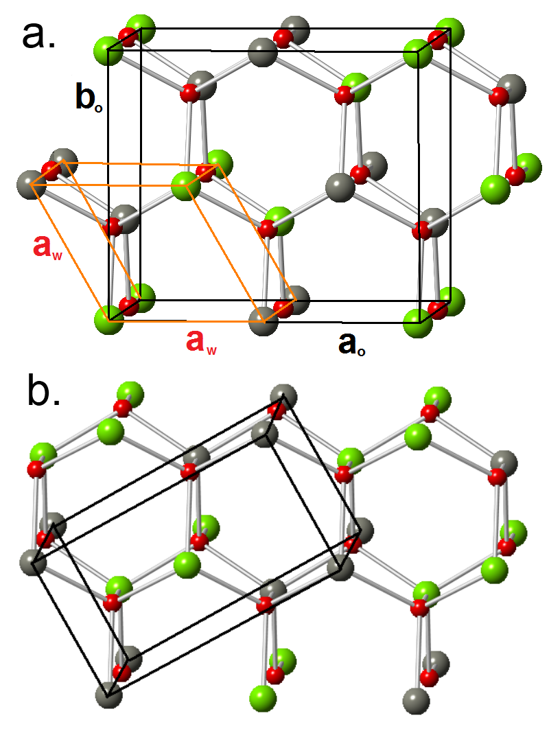
There is another model for disorder on the cation sublattice that does not produce octet rule violations. In ZnGeN2 and other wurtzite-based heterovalent ternary semiconductors, there are two ways of ordering the cation lattice that preserve the octet rule. One configuration has the space group 21, shown Fig. 1a. The unit cell has sixteen atoms instead of four as for wurtzite, and the symmetry is orthorhombic [6]. The other way of ordering has the space group 21 and an eight-atom unit cell, [7], depicted in Fig. 1b. It has been shown that by randomly stacking 21- and 21-like layers in the crystal’s direction, an effectively disordered structure is formed without producing any octet-rule violations [1]. This alternative model of cation disorder could explain why ZnSnN2 grown by Quayle is observed to be disordered, as evidenced by XRD, but also has a band gap, measured by photoluminescence excitation spectroscopy and by photoluminescence spectroscopy, that is consistent with that predicted for perfectly ordered ZnSnN2 [8, 1]. Similarly, there are two ways of ordering zincblende-based heterovalent ternary compounds, and a similar model of disorder has been presented for these materials [9, 10].
1.2 Detection of Ordering
The x-ray diffraction (XRD) and Raman spectroscopy measurements used in the present study can differentiate between ordered and disordered material, but not whether the disorder obeys or violates the octet rule.
Ordering of heterovalent ternary semiconductors is usually detected through XRD. For ternary semiconductors derived from both zincblende and wurtzite lattices, there is often a lattice distortion associated with the cation lattice ordering. In chalcopyrite structures can deviate from the zincblende value of 2 [11]. In wurtzite-derived orthorhombic structures with space group 21, the parameter increases and the parameter decreases, causing to become greater than the ideal wurtzite value of . These distortions, if large enough, can be detected using XRD through the splitting of many of the peaks.
In the parent binary zincblende and wurtzite structures there are reflections which are extinguished due to the symmetry of the structures. In disordered heterovalent ternary compounds these reflections are similarly extinguished through destructive interference arising from the disordered cation sublattice. Superstructure peaks in the XRD pattern appear when the symmetry is reduced due to cation ordering. The superstructure peaks can be very weak, however, because their presence depends on the difference in scattering cross section between the two cation types. In chalcopyrite, the (101), (217), and (611) peaks are typical superstructure reflections that appear upon ordering [12]. In orthorhombic 21, the (110) and (101) peaks are the strongest superstructure peaks. In ZnGeN2 these superstructure peaks are approximately two orders of magnitude less intense than the strongest peaks, while for ZnSnN2, they are only one order of magnitude less intense [1].
Order-disorder transitions have been observed in many zincblende-based heterovalent ternary semiconductors. At temperatures much lower than the melting temperatures of the compounds, the structure is chalcopyrite. As the temperature is raised, a disorder transition is observed for some compounds, often 50-80∘C below the melting point, as evidenced by XRD. For other compounds, the material melts before the order-disorder transition is observed [11].
There has been much less research reported on ordering in the wurtzite-based heterovalent ternary compounds. ZnGeN2 and ZnSiN2 [13] have been grown with ordered 21 lattices. ZnSnN2 was first synthesized just a few years ago [14, 8] and has been receiving more interest lately as a potential earth-abundant solar absorber. Unambiguous observations of 21 ordering in ZnSnN2 have not yet been reported. Identification of ordering through the XRD peak-splitting is more difficult for ZnSnN2 than for ZnGeN2 and ZnSiN2 because the amount of structure distortion due to ordering, for example the deviation of the b/a ratio from that of ideal wurtzite, is predicted to be smaller. For ZnGeN2 the b/a ratio is 2.2% smaller than the wurtzite value, while the b/a ratio of ZnSnN2 is predicted to be within 0.1% of the wurtzite value [1]. On the other hand the (110) and (101) superstructure peaks associated with 21 ordering in ZnSnN2 are predicted to be an order of magnitude larger than in ZnGeN2 [1], but they have not yet been reported to be observed. Kawamura et al. report on a high pressure synthesis method that enabled the growth of polycrystalline ZnSnN2 at a higher temperature (800∘C) than has been possible before [15]. The XRD pattern showed sharp peaks indicating high crystalline quality, but the superstructure peaks were still absent. A recent report of ZnSnN2 grown on LiGaO2 showed some structural distortion that the authors attributed to ordering [16]. Other reports show evidence of control of parameters such as the band gap and carrier concentration [17, 18, 5, 19] by varying growth conditions and by annealing. While these studies have made progress in the improvement of the quality of the ZnSnN2, definitive XRD evidence of cation ordering is still absent. More research is needed to determine the effects of ordering in ZnSnN2 and how to control it.
A range of ordering has been observed for ZnGeN2, but until recently it has not been understood how to control the cation lattice ordering [20, 21, 22, 23, 13, 24, 25, 26, 27, 28]. The present study shows that ZnGeN2 grown at lower temperatures tends to have a high degree of disorder on the cation sublattice, while at higher temperatures the cation sublattice becomes ordered. In addition, annealing of disordered material at high temperature causes the cation sublattice to order. Recently, Shang et al. reported temperature-dependent ordering in ZnGeN2 produced by annealing Zn2GeO4 under NH3. Their observations are consistent with the present study [29].
In section 2 of this paper, the growth methods and the experiments probing the control of ZnGeN2 cation lattice ordering are described. In section 3, the XRD and Raman results demonstrating the variation and control of ordering are reported and their implications are discussed.
2 Materials and Methods
In this fundamental study, ZnGeN2 was grown by a vapor-liquid-solid method involving the use of either a liquid Zn-Ge alloy or a liquid Zn-Ge-Sn alloy, with Sn serving in the latter case as a diluent, reacting with gaseous NH3 in the center of a single-zone quartz tube furnace. While the material produced in these studies was polycrystalline, these types of growth methods in general can serve as possible routes to producing large single crystals and are therefore are of interest as potential methods for producing high quality substrates.
In the first set of growth experiments, Zn vapor and NH3 (Airgas Research Grade) flowed over a [111]-oriented Ge wafer resting on a graphite platform. In a slightly modified second set of experiments designed to explore the effect of the addition of Sn, a Sn/Ge liquid in equilibrium with a solid Ge wafer was exposed to Zn vapor and NH3. In GaN growth, the addition of diluent metals such as Na to Ga has been shown to alter the kinetics of the growth [30]. For all of the experiments Zn vapor was supplied by evaporating liquid Zn (Alfa Aesar 99.999% purity) from a graphite crucible on the upstream side of the furnace. The Zn partial pressure was controlled by adjusting the crucible position, and thereby the crucible temperature, via a bellows-sealed plunger. The Ge wafer platform and the Zn crucible temperatures were monitored using type-K thermocouples embedded in the graphite pieces. The Ge wafer platform temperature was calibrated at the melting temperatures of Sn (232∘C) and Al (660∘C) by observing the change in slope of the temperature-versus-time profile associated with the heat of solidification during cooling. The temperature was calibrated to within approximately 5∘C. H2 from a hydrogen generator (Matheson Chrysalis II) was used as the carrier gas. Gas purifiers (Entegris Gatekeeper) were used at the points of injection for the H2 as well as the high purity N2 and NH3.
2.1 Growths on Ge wafers
Table 1 lists the conditions for a series of four growth experiments on Ge substrates. Prior to being loaded into the chamber, the Ge wafer and Zn were chemically etched to reduce surface oxides. Zn shot (Alfa Aesar 99.999% purity) was melted into a slug, allowed to cool, then was etched in 6:1 H2O:HNO3 for one minute. The Ge wafer was etched in 10% HF for one minute. To reduce atmospheric O2 and H2O contamination in the growth chamber, a series of pump-and-purge operations was performed before each experiment. After the Zn and Ge were loaded into the quartz tube, 500 sccm of N2 was flowed at 0.013 atm for 1 hour, then, the H2 and NH3 lines were purged by flowing 120 sccm and 60 sccm of H2 and NH3, respectively, at 0.013 atm for 0.5 hours. To ensure effective purging of the chamber, including stagnant volumes, the pressure was increased to atmospheric pressure with N2 then evacuated to 0.013 atm. Five of these pump-purge cycles were performed. Subsequently, the furnace was heated to 400∘C while flowing 50 sccm H2 for approximately 16 hours. This step further reduced atmospheric contamination and accelerated water desorption from chamber walls and reduction of oxides on the Zn and Ge surfaces.
The furnace was then raised to the growth temperature under 60 sccm of H2 flow at 0.94 atm with the Zn crucible pulled out of the furnace. The temperature was maintained for 0.5 hours to let the temperature gradients at the ends of the furnace equilibrate. The Zn crucible was then pushed into the furnace to the location at which the desired Zn temperature was reached. Once the Zn temperature equilibrated, the NH3 flow was started in order to initiate ZnGeN2 growth. For all of the experiments, the total flow rate during the growth stage was 60 sccm. The gas flow rates were maintained during the cooling stage.
2.2 Annealing Experiments
For the annealing experiments, disordered ZnGeN2 was grown using the conditions shown in Table 1 for growth experiment 1. After XRD and Raman measurements were performed, the disordered material was loaded back into the chamber for annealing. The pump-purge cycles described in section 2.1 were performed before flowing 100 sccm N2 at 0.013 atm for approximately 16 hours at room temperature, rather than at the 400∘C temperature used for the growth experiments, in order to avoid decomposition of the ZnGeN2.
At high temperature the rate of decomposition of the ZnGeN2 was found to be sensitive to the ambient gas composition. From separate experiments it was determined that if ZnGeN2 was heated to 850∘C in 0.94 atm of pure N2, all of the ZnGeN2 would decompose within one hour, leaving pure Ge on the wafer. Annealing at 850∘C in 0.94 atm of pure NH3 resulted in complete conversion to Ge3N4 in one hour, as evidenced by XRD analysis. Therefore, in order to avoid decomposition of ZnGeN2 during annealing, Zn vapor and NH3 were flowed while at high temperature, at the partial pressures shown in Table 1. Analysis by optical microscopy before and after annealing under these conditions confirmed that the ZnGeN2 crystals were unchanged in size and shape and that therefore additional ZnGeN2 was not grown during the annealing experiments. As anticipated, the layer of ZnGeN2 already present prevented Ge from reaching the surface to react with the ambient Zn and NH3. Table 1 lists the conditions for the two annealing experiments.
2.3 Growth on a Ge/Sn Liquid
A modified version of the growth method described in section 2.1 consisted of growing ZnGeN2 on a Ge/Sn liquid. A shaving of Sn (Alfa Aesar 99.999%) approximately 0.05 g in mass was placed on the Ge wafer prior to being loaded into the furnace. Upon heating to the growth temperature of 758∘C, a liquid alloy formed that was in equilibrium with the solid Ge wafer. After the furnace reached the desired temperature, the Zn crucible was pushed into the furnace and heated to the desired temperature. As the Zn partial pressure was increased, Zn dissolved into the Ge/Sn liquid. The Ge/Sn liquid was left exposed to the Zn pressure for 15 minutes in order for the liquid composition to equilibrate before flowing NH3. At the growth conditions, the liquid composition was estimated to be approximately 31 at.% Sn, 15 at.% Zn, and 54 at.% Ge, based on thermodynamic data [31, 32, 33].
2.4 Characterization Methods
Powder x-ray diffraction measurements were done with a Bruker Discover D8 with a 2-dimensional detector.
For Raman spectroscopy measurements, either a 633 nm or a 532 nm wavelength laser beam was sent through a 50x objective onto the sample. The beam was defocused so that an area approximately 70 m wide was illuminated. The scattered light was collected in reflection by the same objective, filtered, and detected by a spectrometer equipped with a liquid-nitrogen-cooled CCD.
3 Results
3.1 Growths on Ge wafers
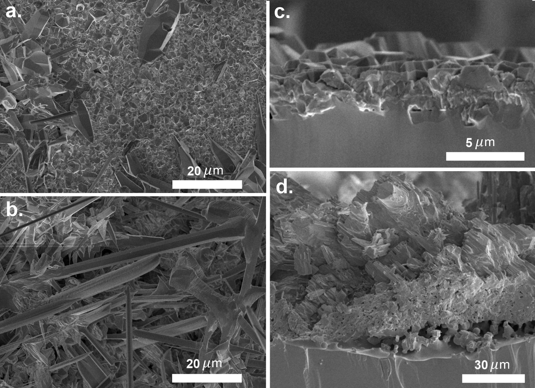
Figures 2 and 2 show SEM micrographs of the surfaces of growth experiments 1 and 3, respectively. Figures 2 and 2 show the cross-sections of the cleaved wafers of growth experiments 1 and 4, respectively. The smooth area at the bottom of the frame in figures 2 and 2 is the underlying Ge wafer. The crust thickness tended to become thicker and the crystallite sizes tended to be larger as the growth temperature was increased.
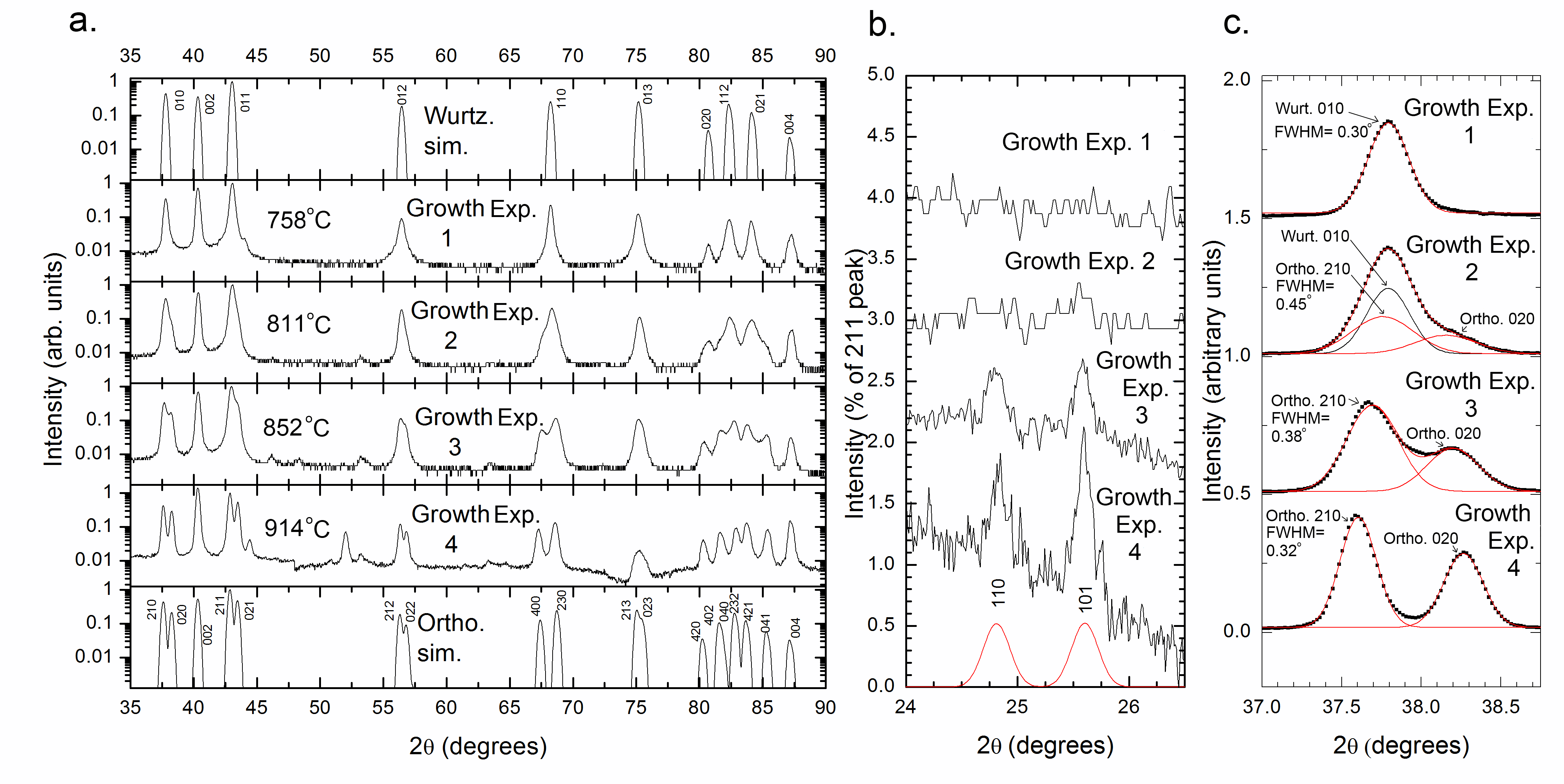
Fig. 3 shows the XRD patterns for the four growth experiments. The simulated patterns were made using Crystal Diffract software using lattice parameters fit from the measured patterns, listed in Table 2. The wurtzite simulation was calculated assuming each cation site had an average occupancy of 50% Ge and 50% Zn atoms. The XRD pattern of growth experiment 1, at the lowest growth temperature, is indistinguishable from that of wurtzite, consistent with this material having a mostly disordered cation sublattice. As the growth temperature was increased, the cation ordering increased, as evidenced by the increased peak splitting observed in the figure. Fig. 3c shows the (210) and (020) peaks with an expanded x-axis. The patterns were fit using Gaussian curves in order to derive the lattice parameters. It is clear that the peak splitting increased with growth temperature, but the resulting pattern was not always fit well by a single phase. Since there are twice the number of (210) planes as (020) planes in ordered ZnGeN2, the (210) peak should be twice the height of the (020) peak. Growth experiment 2 does not have this 2:1 ratio. Instead, the pattern of growth experiment 2 was fit well by a mixture of an ordered orthorhombic phase and a disordered wurtzite phase. In the fit, the orthorhombic phase was constrained to have a 2:1 intensity ratio for the (210) and (020) peaks, and the wurtzite phase was constrained to have the same lattice parameter and peak width as the disordered material of growth experiment 1. Researchers studying ZnSnP2 also found evidence of phase separation of the ordered chalcopyrite and disordered sphalerite structures [3]. Growth experiments 3 and 4 were each fit well by the single orthorhombic 21 phase.
| Expt. | Growth Temp. (0C) | PZn (atm) | PNH3 (atm) | PH2 (atm) | PN2 (atm) | Duration (hours) |
|---|---|---|---|---|---|---|
| Growth exp. 1 | 758 | 0.027 | 0.31 | 0.63 | 0 | 3.7 |
| Growth exp. 2 | 811 | 0.056 | 0.24 | 0.70 | 0 | 4.0 |
| Growth exp. 3 | 852 | 0.028 | 0.31 | 0.63 | 0 | 1.5 |
| Growth exp. 4 | 914 | 0.028 | 0.47 | 0.47 | 0 | 2.0 |
| Anneal 1 | 850 | 0.03 | 0.47 | 0 | 0.47 | 1.0 |
| Anneal 2 | 850 | 0.03 | 0.47 | 0 | 0.47 | 4.0 |
| Platelet | 758 | 0.03 | 0.31 | 0.63 | 0 | 4.0 |
Equilibrium thermodynamics predicts that the ordered phase is stable at low temperature and the disordered phase is stable at high temperature. The trend observed here with ZnGeN2 is opposite to that predicted by thermodynamics, so we conclude that the equilibrium disorder temperature is higher than the temperatures explored here, and the observed disordered samples are in metastable states. We speculate that at the lower growth temperatures atoms do not have sufficient kinetic energy to overcome barriers to finding the lowest-energy, ordered configuration, while at higher temperatures they do.
The orthorhombic and lattice parameters change as the growth temperature is increased, as indicated by the shifting peaks in Fig. 3. The fitted lattice parameters are shown in Table 2. As the growth temperature increases from that of growth experiment 1, 758∘C, increasing fractions of the cation sublattice become ordered. In the beginning stages of ordering we should expect to see some mixing of ordered and disordered material, which is what we see with growth experiment 2. In these mixtures, regions of ordered ZnGeN2 are in close proximity to regions of disordered ZnGeN2, which has different and parameters, so the and lattice parameters may not be fully relaxed. As the proportion of ordered material increases, the and parameters may be able to more fully relax, resulting in the parameter growing and the parameter shrinking with increasing growth temperature. The inhomogeneous strain that may result from the mixing of ordered and disordered material may be the cause here of the broader XRD peaks observed for growth experiments 2 and 3. As shown in Fig. 3c, the deconvolved 21 (210) peak is absent for growth experiment 1, widest for growth experiment 2, then narrows as the material becomes more completely ordered at higher growth temperatures. Modeling of powder diffraction patterns in CrystalDiffract was done to estimate the strain in the samples. For growth experiment 1, a strain of 0.11 (+/-0.03) % was consistent with the change in peak width with scattering angle. For growth experiment 3, a strain of 0.18 (+/-0.05) % was found. For the highest temperature growth experiment 4, a strain of 0.11 (+/-0.03) % was found.
| Expt. | a (Å) | b (Å) | c (Å) |
|---|---|---|---|
| Growth exp. 1 | 6.383 | 5.523 | 5.192 |
| Growth exp. 2 | 6.41 | 5.477 | 5.189 |
| Growth exp. 3 | 6.43 | 5.468 | 5.190 |
| Growth exp. 4 | 6.450 | 5.462 | 5.193 |
| Anneal 1 | 6.42 | 5.486 | 5.190 |
| Anneal 2 | 6.43 | 5.476 | 5.190 |
| Platelet | 6.44 | 5.468 | 5.191 |
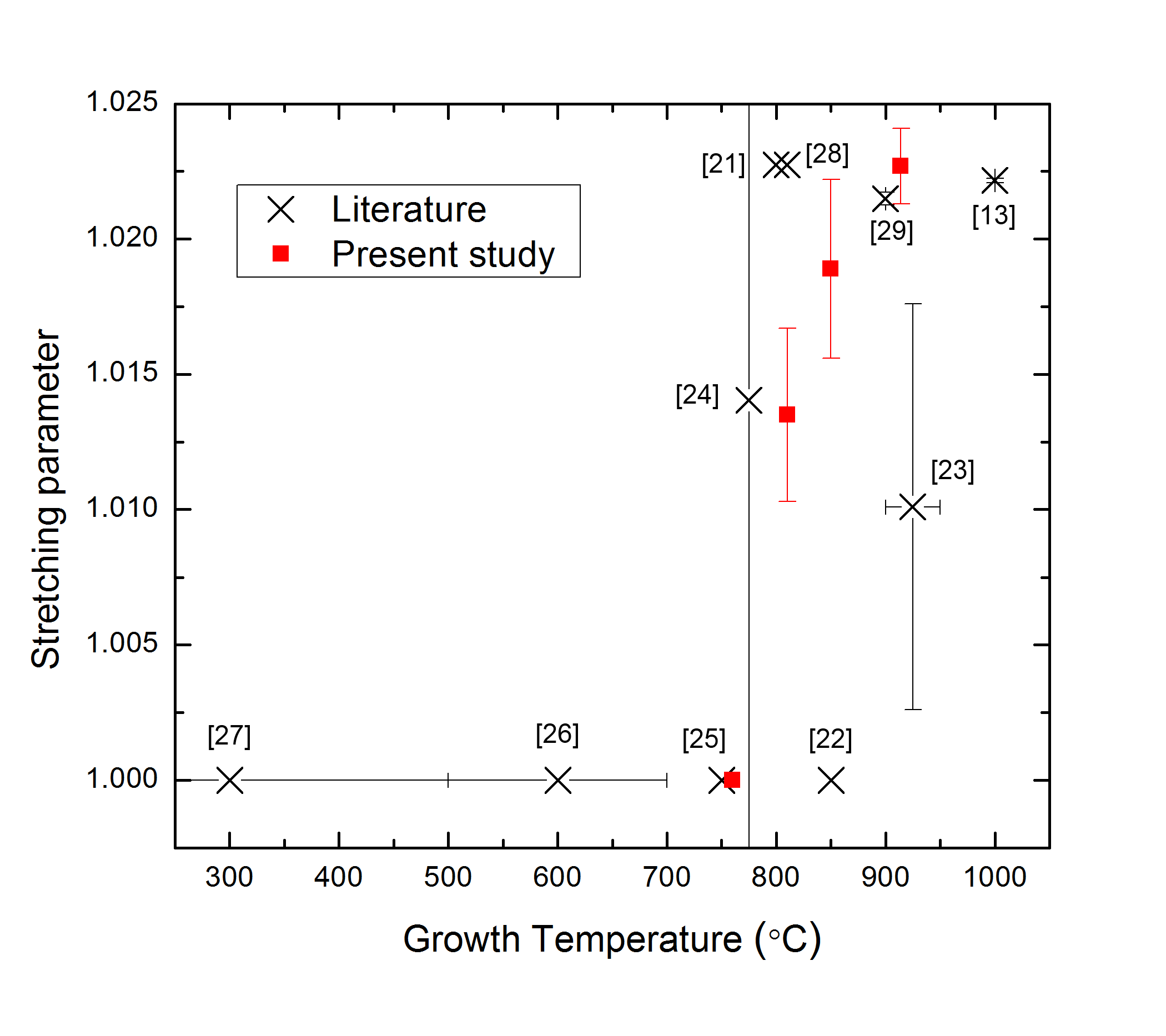
Here we compare the lattice parameters of ZnGeN2 in the literature to our results, as functions of growth temperature. We introduce the stretching parameter, , where and are the orthorhombic lattice parameters, to quantify the orthorhombic cation lattice ordering. A wurtzite structure viewed in the orthorhombic unit cell has an ratio of , so disordered material has equal to 1, and partially or fully ordered material has greater than 1. Fig. 4 plots the stretching parameter for the four growths on Ge wafers in the present study and for ten ZnGeN2 growths reported in the literature, as a function of growth temperature. All of the ZnGeN2 lattice parameters reported in the literature were converted to the orthorhombic system for ease of comparison. Below growth temperatures of approximately 760∘C, all reported material is disordered (wurtzite-like). Above this temperature, almost all material is reported to have some amount of orthorhombic ordering.
Fig. 3b shows, for the material reported here, the portion of the XRD pattern containing the (110) and (101) superstructure peaks. The pattern for growth experiment 1 shows no superstructure peaks, consistent with that material being mostly disordered. The pattern of growth experiment 2 shows small peaks consistent with partial ordering. The patterns of growth experiments 3 and 4 show (110) and (101) peak heights consistent with the prediction for fully ordered 21 material, using atomic positions from [6]. To our knowledge measurement of these superstructure peaks for ZnGeN2 using XRD has not been reported by any other group to date.
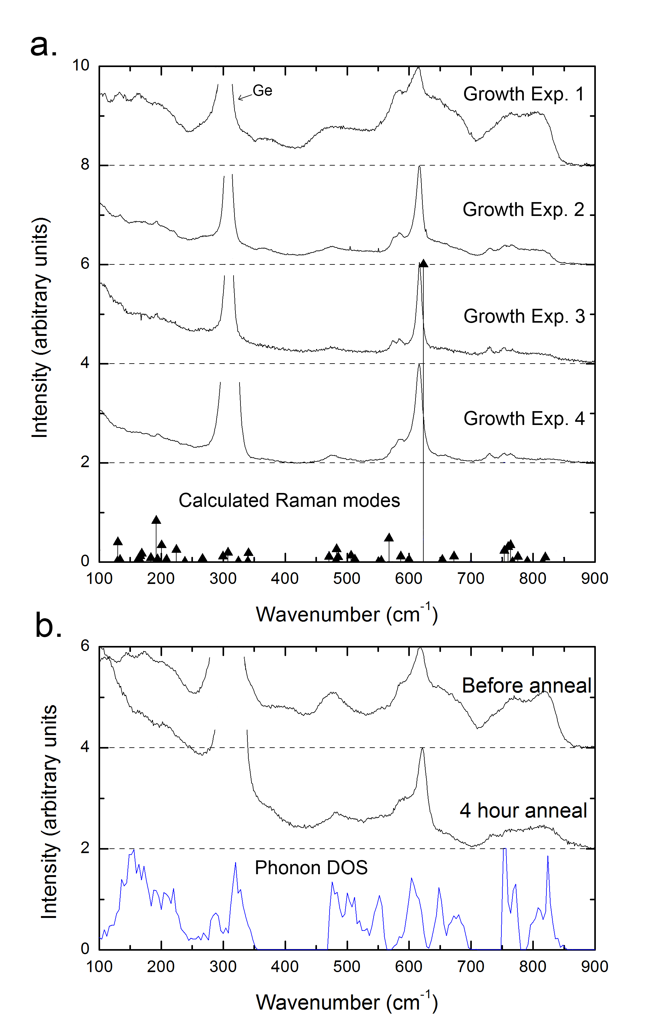
Disorder on the cation lattice disrupts the phonon modes of ordered ZnGeN2, and therefore Raman spectroscopy can be used as an additional method to probe the disorder. In a previous study on single crystal ZnGeN2, strong DOS features were observed in the Raman spectra and were interpreted as arising from the partial breakdown of momentum conservation rules due to disorder [35]. The trends observed here are consistent with this interpretation. The micro-Raman spectra for the four growth experiments are shown in Fig. 5. The spectra are normalized so that the large peak at 616 cm-1 in each spectrum has the same intensity relative to the background above 850 cm-1. As the growth temperature is decreased, the sharpness of the observed peaks decreases and the phonon DOS features increase in intensity. As the disorder increases, the momentum conservation rules are relaxed and phonons from across the Brillouin zone participate in the scattering. The trend toward greater ordering with higher growth temperature observed here in the Raman spectra is consistent with that observed in the XRD patterns.
3.2 Annealing Experiments
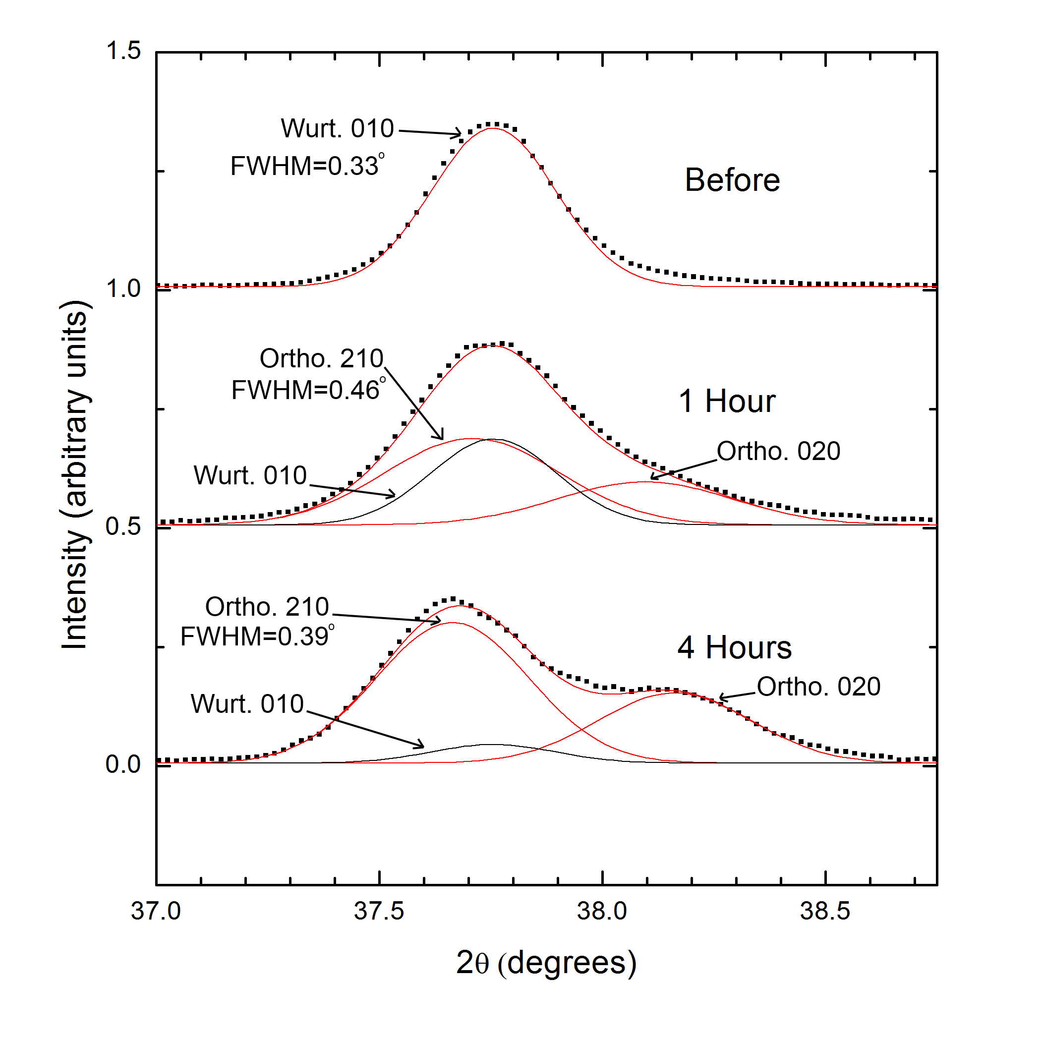
Disordered ZnGeN2 samples were annealed at 850∘C for either one or four hours in the presence of Zn and NH3 vapor. Fig. 6 shows the (210) and (020) XRD peaks for the material before and after the annealing experiments. The first pattern is fit well by wurtzite, consistent with the material being mostly disordered. Peak splitting is evident after one hour of annealing and increases after four hours, consistent with the material becoming increasingly ordered with longer annealing time. The peaks were fit with Gaussian curves to find the lattice parameters as for the analysis described in section 3.1.
3.3 Platelets
Both the ordering and morphology of ZnGeN2 were affected substantially when Sn was added to the Ge wafer. Without Sn, the growth rate along the axis was more than an order of magnitude larger than along the and axes, and hexagonally faceted rod-shaped structures resulted. When Sn was added the growth rate along the and axes was one to two orders of magnitude higher than along the axis, resulting in platelet-like structures. Fig. 7 a. shows a SEM micrograph of the ZnGeN2 platelets. The specific reasons for the change in morphology with the addition of Sn are not understood at this time.
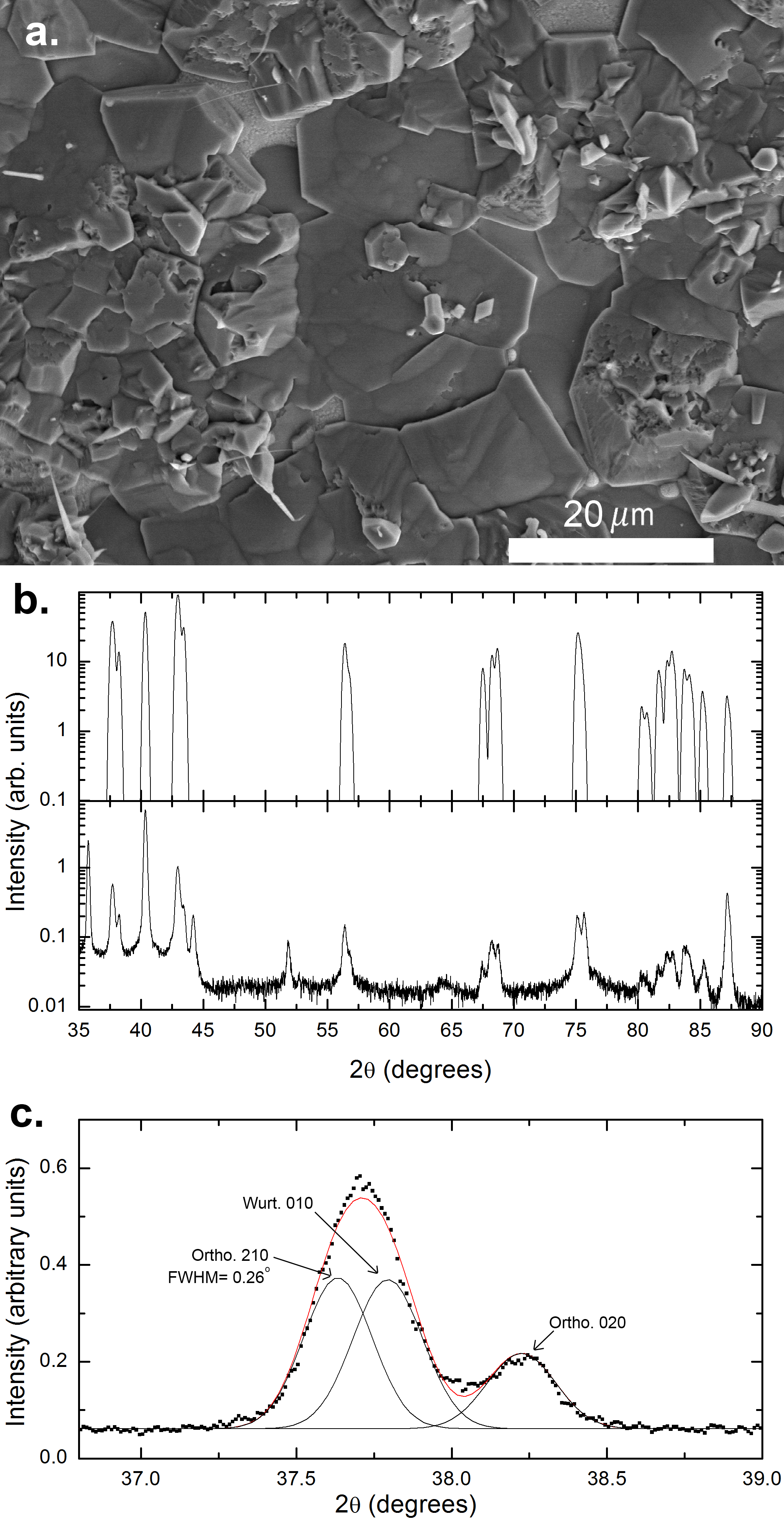
In addition to ZnGeN2, some trace amounts of ZnO grew as evidenced in the XRD pattern. ZnO was not present in any of the growths done without Sn present. We hypothesize that the presence of Sn catalyzes the growth of ZnO from remaining impurities. The ZnO was removed by etching the sample in a 2.5% HCl:water solution for six minutes. The XRD pattern shown in Fig. 7 was taken after the ZnO was removed.
Growing on the Sn liquid resulted in cation lattice ordering at a lower growth temperature when compared with the growths directly on Ge wafers. Fig. 7b shows the XRD pattern of the platelets, grown at 758∘C, which is the same temperature as growth experiment 1 on a Ge wafer in section 3.1. The platelets are much more ordered, as evidenced by the XRD pattern, while the material grown at the same temperature directly on a Ge wafer (Growth experiment 1) is mostly disordered. The XRD pattern of the platelet crystals is a mixture of ordered orthorhombic and disordered wurtzite phases. The peaks in Fig. 7 were fit according to the procedure in section 3.1. During the XRD measurement the sample was rotated in order to assure random sampling of the planes perpendicular to the c-plane. The specific reasons for the change in the tendency to order are not understood at this time but might be related to the change in preferential growth direction.
ZnGeN2 and ZnSnN2 can in principle be alloyed together, and alloys have been synthesized by RF sputtering [37]. Therefore, we must consider the possibility that the material grown in the presence of Sn is a ZnGeN2-ZnSnN2 alloy. Comparing the parameter of the platelets in Table 2 with the other samples reveals that they are equal within the uncertainty of the measurements. Using Vegard’s law, the uncertainty in the parameter of 0.004 is equivalent to a ZnSnN2 volume fraction of 01.5%.
4 Conclusions
These synthesis experiments showed that it is possible to control the cation lattice ordering of ZnGeN2 by varying the growth temperature and by annealing. The material was disordered at the lowest temperature growth experiment (758∘C) and became progressively more ordered as the growth temperature was increased to 914∘C. The equilibrium disorder transition temperature is most likely significantly higher than the temperatures explored here, and so the disordered samples observed here are most likely in metastable states. Growth or annealing at higher temperatures resulted in material closer to the equilibrium ordered 21 state. Ordering was detected using the peak splitting and appearance of superstructure peaks in the measured XRD patterns. The trend between disorder and increase of phonon DOS features in Raman spectra was consistent with the trend observed with the XRD patterns.
Growth on a Sn-based liquid decreased the temperature at which ordered ZnGeN2 was produced. This modified growth method also changed the crystal morphology, resulting in hexagonal platelets instead of hexagonally faceted rod-shaped crystals.
5 Acknowledgements
E.B. and K.K. were supported by the National Science Foundation grants DMR-1006132 and DMR-1409346. J.S. and K.H. acknowledge support from the National Science Foundation grant DMR-1106225.
References
References
-
[1]
P. C. Quayle, E. W. Blanton, A. Punya, G. T. Junno, K. He, L. Han, H. Zhao,
J. Shan, W. R. L. Lambrecht, K. Kash,
Charge-neutral
disorder and polytypes in heterovalent wurtzite-based ternary semiconductors:
The importance of the octet rule, Phys. Rev. B 91 (2015) 205207.
doi:10.1103/PhysRevB.91.205207.
URL http://link.aps.org/doi/10.1103/PhysRevB.91.205207 - [2] W. R. L. Lambrecht, A. Punya, Heterovalent ternary II-IV-N2 compounds: perspectives for a new class of wide-band-gap nitrides, in: B. Gill (Ed.), III-Nitride Semiconductors and their Modern Devices, Oxford University Press, 2013, pp. 519–585. doi:10.1093/acprof:oso/9780199681723.001.0001.
- [3] P. St-Jean, G. Seryogin, S. Francoeur, Band gap of sphalerite and chalcopyrite phases of epitaxial znsnp2, Applied Physics Letters 96 (23) (2010) 231913.
- [4] M. Buerger, The temperature-structure-composition behavior of certain crystals, Proc. Natl. Acad. Sci. 20 (1934) 444.
- [5] T. D. Veal, N. Feldberg, N. F. Quackenbush, W. M. Linhart, D. O. Scanlon, L. F. Piper, S. M. Durbin, Band gap dependence on cation disorder in znsnn2 solar absorber, Advanced Energy Materials 5 (24).
-
[6]
A. Punya, W. R. L. Lambrecht, M. van Schilfgaarde,
Quasiparticle band
structure of zn-iv-n2 compounds, Phys. Rev. B 84 (2011) 165204.
doi:10.1103/PhysRevB.84.165204.
URL http://link.aps.org/doi/10.1103/PhysRevB.84.165204 - [7] L. Lahourcade, N. C. Coronel, K. T. Delaney, S. K. Shukla, N. A. Spaldin, H. A. Atwater, Structural and optoelectronic characterization of rf sputtered znsnn2, Advanced Materials 25 (18) (2013) 2562–2566.
- [8] P. C. Quayle, K. He, J. Shan, K. Kash, Synthesis, lattice structure, and band gap of znsnn 2, MRS Communications 3 (03) (2013) 135–138.
- [9] S.-H. Wei, L. . G. Ferreira, A. Zunger, First-principles calculation of the order-disorder transition in chalcopyrite semiconductors, Physical Review B 45 (5) (1992) 2533.
- [10] S.-H. Wei, S. Zhang, A. Zunger, Band structure and stability of zinc-blende-based semiconductor polytypes, Physical Review B 59 (4) (1999) R2478.
- [11] L. Garbato, F. Ledda, A. Rucci, Structural distortions and polymorphic behaviour in abc 2 and ab 2 c 4 tetrahedral compounds, Progress in crystal growth and characterization 15 (1) (1987) 1–41.
- [12] S. Francoeur, G. Seryogin, S. Nikishin, H. Temkin, X-ray diffraction study of chalcopyrite ordering in epitaxial znsnp sub 2 grown on gaas, Applied physics letters 74 (24).
- [13] T. Endo, Y. Sato, H. Takizawa, M. Shimada, High-pressure synthesis of new compounds, znsin 2 and zngen 2 with distorted wurtzite structure, Journal of materials science letters 11 (7) (1992) 424–426.
- [14] L. Lahourcade, N. C. Coronel, K. T. Delaney, S. K. Shukla, N. A. Spaldin, H. A. Atwater, Structural and optoelectronic characterization of rf sputtered znsnn2, Advanced Materials 25 (18) (2013) 2562–2566.
- [15] F. Kawamura, N. Yamada, M. Imai, T. Taniguchi, Synthesis of znsnn2 crystals via a high-pressure metathesis reaction, Crystal Research and Technology.
- [16] N. Senabulya, N. Feldberg, R. A. Makin, Y. Yang, G. Shi, C. M. Jones, E. Kioupakis, J. Mathis, R. Clarke, S. M. Durbin, Stabilization of orthorhombic phase in single-crystal znsnn2 films, AIP Advances 6 (7) (2016) 075019.
- [17] A. N. Fioretti, A. Zakutayev, H. Moutinho, C. Melamed, J. D. Perkins, A. G. Norman, M. Al-Jassim, E. S. Toberer, A. C. Tamboli, Combinatorial insights into doping control and transport properties of zinc tin nitride, Journal of Materials Chemistry C 3 (42) (2015) 11017–11028.
- [18] A. N. Fioretti, E. S. Toberer, A. Zakutayev, A. C. Tamboli, Effects of low temperature annealing on the transport properties of zinc tin nitride, in: Photovoltaic Specialist Conference (PVSC), 2015 IEEE 42nd, IEEE, 2015, pp. 1–5.
- [19] N. Feldberg, J. Aldous, W. Linhart, L. Phillips, K. Durose, P. Stampe, R. Kennedy, D. Scanlon, G. Vardar, R. Field III, et al., Growth, disorder, and physical properties of znsnn2, Applied Physics Letters 103 (4) (2013) 042109.
- [20] M. Maunaye, J. Lang, Préparation et Proprietés de ZnGeN2, Mater. Res. Bull 5 (1970) 793.
- [21] M. Wintenberger, M. Maunaye, Y. Laurent, Groupe spatial et ordre des atomes de zinc et de germanium dans ZnGeN2, Mat. Res. Bull. 8 (1973) 1049.
- [22] W. L. Larson, H. P. Maruska, A. Stevenson, Synthesis and Properties of ZnGeN2, J. Electrochem. Soc. 121 (1974) 1683.
- [23] K. Du, C. Bekele, C. C. Hayman, J. C. Angus, P. Pirouz, K. Kash, Synthesis and Characterization of ZnGeN2 grown from Elemental Zn and Ge Sources, J. Cryst. Growth 310 (2008) 1057.
- [24] T. Misaki, A. Wakahara, H. Okada, A. Yoshia, Epitaxial growth and characterization of ZnGeN2 by metalorganic vapor phase epitaxy, J. Cryst. Growth 260 (2004) 1049.
- [25] T. J. Peshek, Studies in the growth and properties of zngen2 and the thermochemistry of gan, Ph.D. thesis, Case Western Reserve University (2008).
- [26] L. Zhu, P. Maruska, P. Norris, P. Yip, L. Bouthillette, Epitaxial Growth and Structural Characterization of Single Crystalline ZnGeN2, MRS Internet J. Nitride Semicond. Res. 4S1 (1999) G3.8.
- [27] S. Kikkawa, H. Morisaka, Rf-sputter deposition of zn–ge nitride thin films, Solid state communications 112 (9) (1999) 513–515.
- [28] R. Viennois, T. Taliercio, V. Potin, A. Errebbahi, B. Gil, S. Charar, A. Haidoux, J.-C. Tédenac, Prospective investigations of orthorhombic ZnGeN2: synthesis, lattice dynamics and optical properties, Mater. Sci. Eng. B 82 (2001) 45–49.
- [29] M. Shang, J. Wang, J. Fan, H. Lian, Y. Zhang, J. Lin, Zngen 2 and zngen 2: Mn 2+ phosphors: hydrothermal-ammonolysis synthesis, structure and luminescence properties, Journal of Materials Chemistry C 3 (36) (2015) 9306–9317.
- [30] H. Yamane, M. Shimada, T. Sekiguchi, F. J. DiSalvo, Morphology and characterization of gan single crystals grown in a na flux, Journal of crystal growth 186 (1) (1998) 8–12.
- [31] B.-J. Lee, Thermodynamic assessments of the sn-zn and in-zn binary systems, Calphad 20 (4) (1996) 471–480.
- [32] Z. Long, F. Yin, Y. Liu, J. Wang, H. Liu, Z. Jin, Thermodynamic description of the ru-(si, ge)-sn ternary systems, Journal of phase equilibria and diffusion 33 (2) (2012) 97–105.
- [33] R. Olesinski, G. Abbaschian, The ge-zn (germanium-zinc) system, Journal of Phase Equilibria 6 (6) (1985) 540–543.
-
[34]
[link].
URL http://www.crystalmaker.com/crystaldiffract/ -
[35]
T. J. Peshek, T. R. Paudel, K. Kash, W. R. L. Lambrecht,
Vibrational modes in
ZnGeN2: Raman study and theory, Phys. Rev. B 77 (23) (2008) 235213.
doi:10.1103/PhysRevB.77.235213.
URL http://link.aps.org/abstract/PRB/v77/e235213 -
[36]
T. R. Paudel, W. R. L. Lambrecht,
First-principles study
of phonons and related ground-state properties and spectra in Zn-IV-N2
compounds, Phys. Rev. B 78 (11) (2008) 115204.
doi:10.1103/PhysRevB.78.115204.
URL http://link.aps.org/abstract/PRB/v78/e115204 - [37] P. Narang, S. Chen, N. C. Coronel, S. Gul, J. Yano, L.-W. Wang, N. S. Lewis, H. A. Atwater, Bandgap tunability in zn (sn, ge) n2 semiconductor alloys, Advanced Materials 26 (8) (2014) 1235–1241.