Small slot waveguide rings for on-chip quantum optical circuits
Abstract
Nanophotonic interfaces between single emitters and light promise to enable new quantum optical technologies. Here, we use a combination of finite element simulations and analytic quantum theory to investigate the interaction of various quantum emitters with slot-waveguide rings. We predict that for rings with radii as small as 1.44 m (Q = 27,900), near-unity emitter-waveguide coupling efficiencies and emission enhancements on the order of 1300 can be achieved. By tuning the ring geometry or introducing losses, we show that realistic emitter-ring systems can be made to be either weakly or strongly coupled, so that we can observe Rabi oscillations in the decay dynamics even for micron-sized rings. Moreover, we demonstrate that slot waveguide rings can be used to directionally couple emission, again with near-unity efficiency. Our results pave the way for integrated solid-state quantum circuits involving various emitters.
pacs:
I Introduction
The cutting edge of solid-state quantum optics is determined by our ability to realize phenomena such as photon-mediated cooperative effects between multiple quantum emitters Greentree et al. (2006); Chang et al. (2008); Carusotto et al. (2009); Angelakis et al. (2011), few-photon nonlinearities Loo et al. (2012); Maser et al. (2016); Martín-Cano et al. (2014), and strong light-matter coupling Reithmaier et al. (2004); Yoshie et al. (2004), which provide the resources that are crucial for scalable quantum simulation and information processing Weimer et al. (2010); Lodahl et al. (2015); Pichler et al. (2015). An important bottleneck in this endeavor is the efficient coupling of light and matter. Ideally, one would like a single photon to interact with a single quantum emitter such as a quantum dot, color center, ion, or molecule with 100% efficiency.
Traditionally, cavities have been used to boost light-matter coupling by significantly increasing the time during which a photon and an emitter interact. A variety of resonators such as bulk Fabry-Pérot cavities, microspheres, microdisks, micropillars, or photonic crystal cavities can retain a photon for millions of optical cycles, increasing the probability that a photon interacts with a quantum emitter to unity Vahala (2003). In other words, a photon is always emitted into the cavity mode. The high quality factors (Q) required for this operation, however, usually pose severe technical challenges. In particular, it becomes imperative that one tunes the narrow resonances of the cavity and the emitter to each other and stabilizes the cavity length to down to a few picometers Münstermann et al. (1999). Simultaneous coupling of several emitters or frequencies that can be individually addressed is, therefore, not within reach.
As an alternative to cavity-enhanced interaction, several groups have investigated single-pass coupling via near-field optics Gerhardt et al. (2007), tight focusing Vamivakas et al. (2007); Wrigge et al. (2008); Tey et al. (2008); Streed et al. (2012) or a subwavelength waveguide (nanoguide) Shen and Fan (2005); Vetsch et al. (2010); Yalla et al. (2012); Faez et al. (2014). The key concept in this approach is spatial mode matching between the photon and the emitter radiation pattern. Although the coupling efficiency can theoretically reach unity Zumofen et al. (2008), it is a challenge to identify well-behaved coherent transitions known in atomic physics in the solid state. Here, issues such as the quantum efficiency, phonon dephasing, or lossy transitions limit the scattering cross section of a given transition. For example, in the case of organic dye molecules the Frank-Condon and Debye-Waller factors reduce the overall efficiency by about Gerhardt et al. (2007) while for nitrogen-vacancy centers in diamond, strong phonon wings and the quantum efficiency limit the efficiency to well below Santori et al. (2010). In cavity-coupling, one can hope to compensate for such photophysical deficiencies by strong enhancement of the interaction between the cavity mode and the emitter Novotny and Hecht (2012).
The central advantage of a cavity-free coupling is its immense bandwidth. In this work, we provide an example, where the advantages of single-pass and cavity couplings are combined through the design of feedback geometries with moderate . Of the different cavity-free approaches, the nanoguide geometry is particularly attractive for this purpose because it can be implemented on a chip and be used as the building block of quantum optical circuits. Moderate cavity feedback would also be particularly advantages for this platform because it is otherwise a great challenge to achieve a very large index contrasts between the nanoguide and its surrounding, necessary for reaching high factors. So far, this issue has been addressed via slow light photonic crystals Chang et al. (2006); Arcari et al. (2014). Another proposal has been to use slot waveguides Jun et al. (2009); Quan et al. (2009).
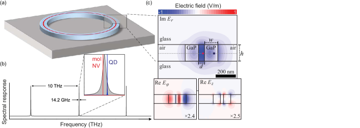
Here, we begin with a slot waveguide that couples well to single quantum emitters and bend it into a ring, as shown in Fig. 1a. We model a realistic implementation of the slot-waveguide ring compatible with nanofabrication capabilities. By choosing a small radius m, we minimize the structure footprint, while keeping the balance between the of the ring and its performance as a quantum optical platform. As we show, this system maintains the broadband nature of waveguides relative to lifetime-limited transitions of solid-state emitter (Fig. 1b) and allows for near-unity and even to enter into the strong coupling regime. We conclude by considering two specific implementations of our system: one where the emitter is sitting inside the slot, as would be the case for single organic molecules or colloidal quantum dots, and the other for an emitter such as a quantum dot or an NV center embedded in one of the high index bars of the slot waveguide (see Fig. 1c). In the latter, we explore the possibility of chiral-emission where the state of the emitter determines in which direction a photon is emitted. In either case, the robust performance of the slot-waveguide ring suggest that it is a powerful platform for future quantum nanophotonic experiments and applications.
II Quantum optics in slot-waveguide rings
II.1 Solid-state quantum emitters in linear nanoguides
Nanoscale waveguides (nanoguides) provide a flexible and scalable platform for quantum optics. The simplest version of a nanoguide consists of a nanoscopic rectangular channel that is surrounded by a lower refractive-index medium, and the efficiency with which it couples to emission depends on the magnitude of this refractive index mismatch. Simply put, a greater refractive index difference between the core and the surrounding results in larger field enhancement inside the nanoguide, and a more efficient interface with a quantum emitter. The optical properties of nanoguides depend on their geometry, meaning that mode profiles, light confinement and bandwidths are all easily tuned. This versatility ensures that nanoguides can be designed to interface with the many different quantum emitters, each of which has different optical properties and is suited for different applications Lounis and Orrit (2005). In practice, however, the coupling efficiency of the system is limited, as its constituent materials are often predetermined by the type of emitter used.
Quantum emitters, in general, act as two (or three) level systems. A transition between these levels occurs as a result of a charge redistribution that can be described by a transition dipole , and is accompanied by the absorption or emission of a photon of angular frequency . Each transition resonance is described by a homogenous linewidth (see Fig. 1b, for a comparison of emitter linewidth relative to a cavity resonance) that is typically distributed over an inhomogeneous spectrum that is typically greater than 1 THz in the solid state. This inhomogeneous broadening arises because each emitter experiences a slightly different local environment within its dielectric host matrix.
Integration of various solid-state emitters in waveguides requires considerations specific to each system. In particular, some emitters such as single organic molecules or colloidal quantum dots are generally embedded in a fairly low index dielectric. Thus, a nanoguide made of the host matrix results in low coupling efficiencies around 0.1 to 0.2 Faez et al. (2014), while inclusion of single molecules or colloidal quantum dots into standard nanophotonic structures fabricated out of high- dielectrics is not trivial either. Rare earth ions, epitaxially grown quantum dots, or vacancy centers in diamond, on the other hand, are inherently embedded in high- matrices that can form nanoguides; The coupling efficiency typically remains below 0.75, though it can be increased by introducing resonances to the structure Fu et al. (2011); Hausmann et al. (2012).
II.2 Straight slot waveguides
Here, we turn to a slot waveguide Jun et al. (2009); Quan et al. (2009); Kolchin et al. (2015), whose cross-cut is outlined in Fig. 1c, showing an ultrathin low region sandwiched between two higher index channels. This geometry leads to an effective coupling of the modes of the two high index channels, resulting in confinement of the propagating mode to the low index region, which is highly subwavelength in size. As a best case, we calculate that an emitter in a 60 nm wide, dielectric between two gallium phosphide (GaP) channels , will experience a coupling efficiency and an enhancement of the emission (see Appendix A for the calculation of and ). These correspond to more than 4-fold increase of and 3-fold increase of relative to a simple nanoguide geometry Faez et al. (2014). The broadband nature of the waveguides results in enhancement of the resonant florescence at , but equally of all red-shifted emission.
II.3 Emission into slot waveguide rings
By bending the slot waveguide into a ring, as shown schematically in Fig. 1a, we can add optical feedback to our system and increase from 0.75 towards unity. The spectral response of a 1.44 m radius ring, where bending losses dominate (see Sec. III.1), is shown in Fig. 1b (other dimensions given in the caption); here, we observe narrow modes separated by 10 THz. A zoom onto the 24th order mode reveals a calculated spectral full-width at half maximum (FWHM) of 14.2 GHz, which is up to 1000 times broader than the natural linewidths of various typical emitter resonances. As examples, in the inset to Fig. 1b we overlay zero-phonon line linewidths of single molecules Jelezko et al. (1996) and vacancy centers in diamond Tamarat et al. (2006) (10-30 MHz FHWM, red curve) and of epitaxially grown quantum dots Matthiesen et al. (2012) (530 MHz, blue curve) over the ring resonance. For this ring geometry, the non-zero width of the resonances is due solely to bending losses, which result in complex eigenfrequencies. Here, for instance, the complex mode frequency is rad/s (calculated using the commercial eigenfrequency solver COMSOL). These bending or radiative losses are the limiting factor of the quality of the resonator given by .
Creating a resonator out of the slot waveguide also affects the optical eigenmode of the structure, albeit in a more subtle manner than the modification to its spectral response. In contrast to a straight slot waveguide, the mode of the ring is slightly asymmetric, as we see in Fig. 1c. This asymmetry is visible in all three field components, as the fields on the outside of the ring (right side) are slightly larger. As is the case for a straight slot waveguide, the field is largest in the slot, where it is also primarily radially polarized. This slot, then, is ideally suited for emitters with linear transition dipoles embedded in a low- dielectric. A good position for such an emitter is marked by the red circle in Fig. 1c; note that this position is clearly off-center, due to the aforementioned mode asymmetry. This slot waveguide ring is also a good platform for emitters that require a high- host dielectric. These, be they epitaxially grown quantum dots or defect centers in diamond, could be placed at the position of the blue square in Fig. 1c (see Sec. IV.2 for a detailed explanation of why such a placement is advantageous).
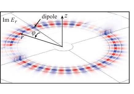
To study the interaction of an emitter with the slot waveguide mode, we perform fully three-dimensional finite element method simulations of the ring structure. A radially oriented transition dipole that oscillates at the ring resonance frequency (i.e. ) represents the emitter, and is placed in the slot. We then look at the steady-state field generated by this dipole, as shown in the and planes in Fig. 2 (where at the position of the dipole), for a m radius ring. In this image the radiation is nearly fully coupled into the photonic modes of the ring. To determine quantitatively, we use the field map, as explained in Appendix A and compute the fraction of the power radiated by a dipole into our nanophotonic system. For the m ring, we calculate that , a 400-fold enhancement of emission with respect to an identical emitter in a straight slot waveguide. Similarly, we calculate by comparing the total emitted power to the one found far along the waveguide. We find , meaning that only 1/200 photons leaks out of the waveguide as compared to 1/4 in a straight nanoguide.
A similar analysis reveals remarkably efficient couplings between the ring and quantum emitters even when they are placed well away from the mode maximum in the slot. An emitter embedded in the high- channel, as shown by the square symbol in Fig. 1c, would experience and (see Sec. IV.2 for more details). That is, slot waveguide rings are compatible with all manner of quantum emitters, including quantum dots or NV centers, which would necessarily be placed out of the field maximum.
In addition to the improvement of the spatial coupling to a single mode, the slot waveguide ring will favor the resonant emission on the zero-phonon line compared to the Stokes-shifted coupling to vibrational states or phonon wings, thus, improving the branching ratio (oscillator strength) of solid-state emitters. This renders a solid-state emitter inside such a ring like an ideal two-level emitter such as an atom with an overall outcome of . Clearly, even a ring with a geometric cross-section of only 6.5 m2 and a moderate acts as a near-ideal interface between an emitter and photons.
II.4 Emission dynamics
We now turn to the dynamics of the emitter-waveguide resonator interaction. In the framework of macroscopic quantum electrodynamics Knöll et al. (2011); Khanbekyan et al. (2008), an emitter that is prepared in its excited state will decay according to (see Appendix B),
| (1) |
where
| (2) |
and . In these equations contains both the loss rate of our nanophotonic resonance and a phase due to detuning between the ring and emitter resonances. In what follows, we assume and hence is simply the loss rate of our system. It follows that depends on the difference between the rate at which energy is lost and the rate at which energy is exchanged between the emitter and the photonic mode.
The dynamics of the emitter’s decay are determined by the interplay between and , which, in turn, are dependent on the resonator quality factor, . Equations (1) and (2) allow us to quantify these dependencies and to calculate the probability to find the emitter in its excited state . The results of these calculations for rings with ranging from 49 to 27900 are shown in Fig. 3(a) (see Sec. III.2 for an explanation on how may be varied by introducing losses into the system). Here, we take MHz, which is typical for a single organic molecule.
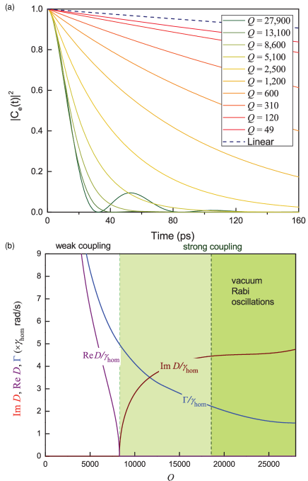
We observe markedly different dynamics for the different rings, ranging from a clear oscillatory behavior for the large rings to a slow exponential decay for small resonators. In other words, the decay dynamics show that these slot waveguide rings can couple either strongly or weakly to quantum emitters, and the coupling strength can be tuned by varying the resonator .
We can, in fact, understand the different coupling regimes by considering Eqs. (1) and (2) and how and depend on [Fig. 3b]. The transition from the strong to the weak coupling regimes occurs when , where evolves from being imaginary to real valued and loses its oscillatory nature. In our system, this change occurs for the moderate value of . For larger resonators, when , Rabi oscillations are clearly visible, as is the case in Fig. 3a.
In contrast, when is real valued, the emitter and resonator photons are weakly coupled and we observe exponential decay dynamics in Fig. 3a. As expected, the decay constant approaches that of an emitter in a straight slot waveguide (dashed curve in Fig. 3a) as decreases. As we shall see below (Sec. IV.1), well into the regime where the resonator and emitter are weakly coupled (where , see Fig. 5), we still find , demonstrating the power of this quantum optical platform.
III Design considerations
The previous sections laid out the response of an idealized slot-waveguide ring, namely one with no losses beyond those associated with the bending of the waveguide. It is fair to ponder how such a ring would fare under more realistic conditions. In this section, we answer this question, first examining the types of imperfections that can be reasonably expected for this type of nanophotonic structure and their consequences to the performance of the ring.
III.1 Nanofabrication: Imperfections and materials
Nanofabrication techniques typically result in imperfections, leading to additional loss channels such as scattering losses due to surface roughness. In addition, depending on the choice of material, dopings or imperfections in the thin dielectric layers can cause absorption losses. The total quality factor of the ring resonator can then be expressed as a sum of three contributions, , corresponding to the radiative, scattering, and absorption channels. For a realistic performance, it is important to examine the competition among these contributions. We choose to neglect absorption losses in this work since several non-absorbing dielectric and semiconductor layers are available. We note, however, that it will be straightforward to extend our results to absorbing material because both absorption and scattering losses effect the optical properties of the ring by limiting the propagation length of the light.
The deposition and nanopatterning of thin films typically results in surface roughness that is on the order of 2-5 nm for granular films (such as TiO2) and can be much smaller for single-crystalline or amorphous materials (such as GaP). In the Rayleigh scattering model, is inversely proportional to both the square of the root-mean-square (RMS) size of surface features and their correlation length Gorodetsky et al. (1996). A realistic value for the surface roughness of 2 nm, with a corresponding correlation length of 10 nm would result in at a wavelength of 760 nm. In fact, it is only when the RMS roughness approaches 10 nm (and the correlation length 100 nm) that drops below 20000.
We also note that although we have used GaP as the high-index medium for our simulations, our findings can be readily transposed to other materials, which might be more suitable for various applications. Three such examples are diamond , SiC , and TiO2 . The lower refractive index contrast between the waveguiding region and the surrounding material lessens the confinement of the light in these cases and causes higher bending losses. To compensate for these, the ring radius can be increased. For example, for a diamond slot waveguide ring with nm, nm and m, we find that . Likewise, for a SiC resonator with nm, nm and m, . In other words, a change in the materials of the slot waveguide can be easily accounted for with a slight tuning of the geometry, allowing us to recover the functionality of our platform.
III.2 Tunability
The optical properties of slot waveguide rings can be changed by tuning the ring geometry (i.e. varying the size to alter ) or by introducing losses, either due to enhanced scattering (e.g. due to surface roughness) or absorption. While scattering is usually a static intrinsic feature, absorption losses can be introduced in either a passive or active manner, e.g., by doping the semiconductor layer during growth or actively by electrical or all-optical generation of free carriers. Active control, in particular, allows for the reshaping of the emitted photon’s wavefunction, if it occurs on the time-scale of the emitter lifetime Jin et al. (2014).
Here, we calculate the eigenmodes of rings (as was done in Fig. 1c), while varying either the ring radius or the imaginary part of the refractive index of GaP, to introduce absorption losses. From these mode distributions and their corresponding complex eigenfrequencies, we extract both and Sauvan et al. (2013) as a function of the ring radius and the propagation length. The outcome is presented in Fig. 4.
As expected, both shrinking the ring and introducing absorption losses leads to a monotonic decrease in (Fig. 4a), here by a factor of almost 300. These calculations show that even resonators with high losses (corresponding to propagation lengths in the 10’s of micrometers) or with radii down to 1 m still have ’s in the 1000’s.
Interestingly, while has a similar dependence on both the radius and the loss, changing these parameters has very different effects on . Decreasing the ring size results in a smaller mode volume (bottom axis, Fig. 4b) although in all cases we observe a small of only a few . This decrease, however, is not proportional to the decrease of the geometric ring volume, where are the outer and inner radii of the ring. For example, a decrease of by a factor of 2.8 results in a corresponding decrease of by only 1.75 (in all cases, ranges from 2.0 to 2.1). This difference occurs because as the ring shrinks, the bending losses increase, and the mode is pushed out of the slot and into the outer part of the ring. The situation is very different when is held constant and losses are ramped up. In this case, the mode distribution is basically unaltered and remains constant (Fig. 4b, top axis).
IV Implementations
In this section we consider two different approaches to quantum optics in a slot waveguide ring. In the first, quantum emitters are embedded at the electromagnetic mode maximum in the low- dielectric in the slot (see Fig. 1c). This approach is compatible with emitters such as single molecules and colloidal quantum dots, and it highlights the strong field confinement inherent to slot waveguides. Secondly, we consider emitters embedded in the high- bars such as epitaxially grown quantum dots or defect centers in diamond. Here, we make use of the structured light fields of the slot waveguide ring to direct emission.
IV.1 Tunability of emission from low- quantum emitters
In Sec. II.3 we saw that slot waveguide rings act as remarkably efficient interfaces between emitters and photons, when the emitters are placed in the field maximum inside the low- slots. Here, we explore the tunability of the emission when the ring properties are varied, as was done in Sec. III.2. We begin by considering the case where absorption losses are introduced. In this case, is changed while the optical eigenmode remains unaltered. The resultant emission properties are displayed in Fig. 5(a). Clearly, both and decrease as the losses increase (see Fig. 4a). The ring, however, maintains its efficient performance for up to 0.004, resulting in and corresponding to a propagation length of 15 m at nm. In this range, while varies between 30 and 1,300.
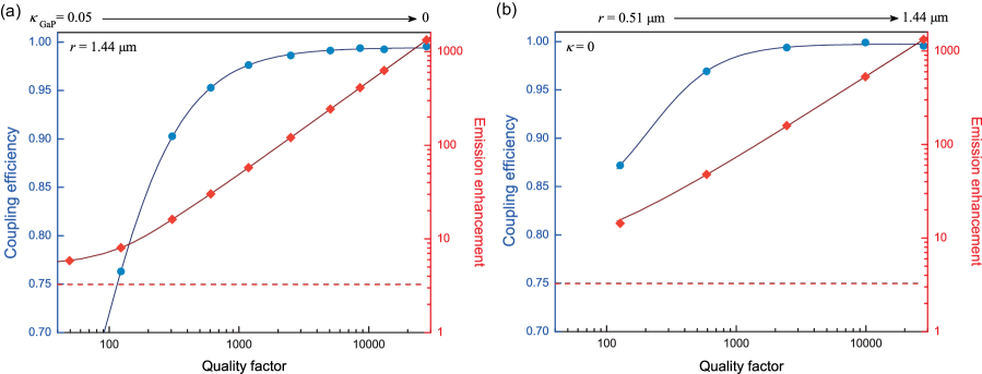
Changing the ring radius instead of introducing losses, affects and in a similar way [Fig. 5(b)]: in both cases, these metrics decrease with decreasing . However, a close inspection of Fig. 5 reveals a difference. The decrease in and is more rapid if is lowered by absorption than if the lowering is caused by the increased radiation losses of the smaller rings because shrinking the ring results in a smaller mode volume, which counteracts the decrease in . In contrast, when absorption losses are introduced decreases while the mode volume remains constant. Since the emission properties depend on the ratio of Novotny and Hecht (2012), we expect a smaller (lossless) ring to outperform a larger, lossy ring with a similar as is most readily noticeable when .
IV.2 Chiral emission with high- quantum emitters
Quantum emitters such as epitaxially grown quantum dots or vacancy centers in diamond, which are embedded in high- dielectrics, can also be interfaced with a slot waveguide ring. As we briefly touched on in Sec. II.3, placing the emitter away from the optical mode maximum necessarily results in a decrease to the emission rate enhancement. For example, an emitter placed in one of the high- channels of a 1.44 m radius ring, as shown by the blue square symbol in Fig. 1c, experiences as compared to at the mode maximum. The emitter does, however, maintain even when placed in one of the high- bars. We now show that at this position, the vectorial nature of light can be exploited to control the direction in which emission occurs. Such unidirectional coupling of emission to photonic pathways can be used as a basis for quantum architecture, and hence has been the focus of several recent studies Mitsch et al. (2014); le Feber et al. (2015); Söllner et al. (2015); Coles et al. (2015).
Unidirectional emission has been investigated for transitions between different spin-states of emitters, whose charge redistribution is described by circular dipoles (e.g. in the ring coordinates). For such directional emission to occur, the optical eigenmodes must contain regions of circular polarization, where the handedness of the light field depends on the direction of propagation. Placing a circular dipole in such a region ensures that it would only radiate in one direction, depending on its handedness. In Fig. 6(a) we show the ellipticity (see Appendix C) of the light field in the m ring [whose mode is shown in Fig. 1(c)]. This quantity is a measure for how circular the light field is, peaking at where the light is right or left handed circularly polarized, while for linear light fields it is 0.
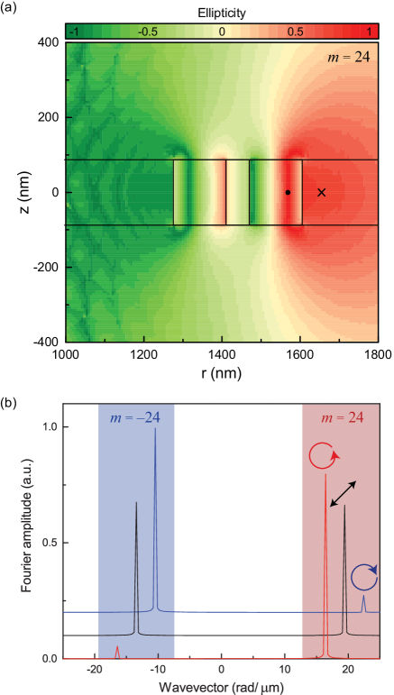
From Fig. 6(a) it is clear that the areas where the light is most circular can be found outside the slot. In fact, since we want both a near-unity ellipticity, as well as a large field amplitude, a favorable position for directional emission is inside the high-index bars (solid circle in Fig. 6a); at this position the ellipticity peaks at 0.87.
We repeat our calculations with an emitter placed at the position marked by the dot in Fig. 6(a). We vary the transition dipole to consider linear as well as right and left handed circularly polarized dipoles. We Fourier transform the line-trace of along the center of the slot to obtain the wavenumber spectrum, whose amplitude is shown in Fig. 6(b). In this transform, we observe two sharp peaks, centered about radm, corresponding to light propagating in the modes, respectively. By comparing the area under these peaks, we determine the directionality of the emission. In the case of the linear dipole (black curve), the two peaks are almost identical and there is no directionality to within a calculation error. In contrast, for the two circular dipoles (blue and red curves), one peak in each curve dominates, depending on the handedness of the dipole. We obtain a directionality of , as expected from the ellipticity of the mode. For completeness, we also calculate the situation of a circular dipole placed in the low index material outside the slot waveguide (cross in Fig. 6a), finding a directionality of .
A slot-waveguide ring, therefore, ideally lends itself as an element in a chiral quantum network Pichler et al. (2015). An emitter such as a quantum dot would experience , which can be decomposed to and for the two counter-propagating modes. We expect that slight adjustments to the waveguide geometry would increase the ellipticity close to unity, and hence allow for perfect directional emission. Finally, we note that the calculated for such an emitter would, for example, sufficiently broaden the emission spectrum and overcome residual line broadenings often encountered in the solid state.
V Conclusions
In this work we introduced the use of slot waveguide rings for quantum optics. We combined numerical models with analytic quantum theory to study the emission properties of single emitters coupled to the rings. We demonstrated that using rings that can realistically be fabricated, with a geometric footprint as small as 6.5 m2, it is possible to strongly couple a solid-state quantum emitter such as an organic dye molecule to the photonic modes. In particular, Rabi oscillations can be clearly visible in the decay dynamics of such moderate rings.
We also showed that it is possible to tune emission properties by changing the optical mode of the slot waveguide rings. Two different tuning mechanisms were identified: a change of the ring size or the introduction of absorption to the system. While the former is a passive effect, active control of the later at speeds up to ultrafast time scales offers a fascinating gateway to all-optical control of complex nanophotonic interactions. In either case, tuning the system led to values ranging from 0.75 to near unity and spanning three orders of magnitude up to about 1300.
In closing we discussed the unique potential of slot waveguide rings for unidirectional emission. As examples, positions both inside the high index bars and in the low index medium outside the slot waveguide ring, were identified. Interestingly, strongly directional emission can occur at positions where and . In summary, the combination of efficient emission enhancement with a high degree of tunability suggest a highly attractive platform for both investigations of fundamental quantum phenomena, and for future quantum optics technology.
Appendix A Numerical calculations of and
The power dissipated by the radiation of a dipole is proportional to the out of phase-response of the electric field at its position Novotny and Hecht (2012). Specifically, the power dissipated by a dipole (with dipole moment ) located at point and radiating at a frequency is
| (3) |
where is the field radiated by the dipole. In our scenario, we assume radially oriented transition dipoles and extract the out-of-phase component from simulations. We can then calculate and , which both characterize emission properties in the presence of the nanophotonic structure, and are used in our analytic model to describe the decay dynamics of the emitter.
The emission enhancement is the ratio of the power dissipated by the radiation of a dipole in a nanophotonic structure (subscript ‘nano’) to that of the same dipole, but in bulk media (subscript ‘hom’). That is, for a linear transition dipole, Eq. 3 allows us to write,
| (4) |
We find , by looking at a line trace from the results of the 3D simulations (e.g. Fig. 2), as shown in Fig. 7.
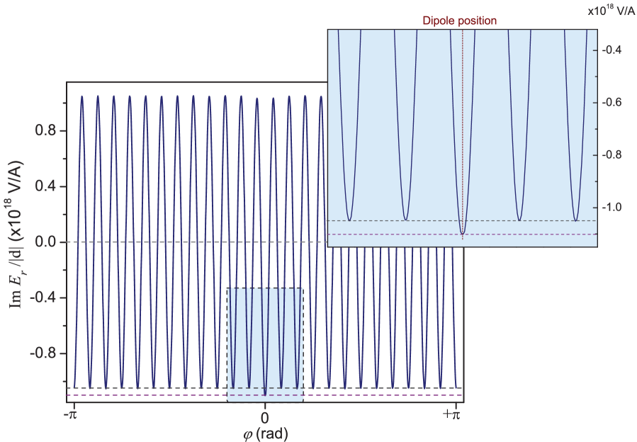
For this ring, V/A. Similarly, for this dipole in bulk naphthalene, we find (using simulations in a half-spherical space, as in the case of the slot waveguide ring) that V/A. Hence, for this particular ring, , as reported in the main text. For completeness, we note that in the weak coupling limit, we can express in terms of the decay rates of the emitter, writing ; in the single mode limit this is equivalent to the Purcell Factor. Sauvan et al. (2013)
To find how well the molecule emits into the desired mode of the ring, we compare at the position of the dipole to that in the far-field of the emitter, but at the same radial distance. This comparison can be seen in Fig. 7, corresponding to the values shown by the dashed purple and dark-gray lines. For this ring () this difference is clearly visible, and it corresponds to .
When large losses are introduced into the system, either due to absorption in the GaP bars or due to increased radiation in small rings, we need to take an extra step to correctly calculate . In the presence of large losses, the radiated field decays away from its source, meaning that there is no constant line-trace to the far-field , as was the case in Fig. 7. In this situation, we fit a decaying exponential envelop function to the field trace using only the far-field field amplitude. The extrapolated value of this envelope function, at the position of the dipole, is then used to calculate .
Appendix B Analytic expression for the
To understand the dynamics of our system we calculate the time-dependent probability to find an emitter inside our slot waveguide ring in its excited state. We develop this expression using the framework of macroscopic quantum electrodynamics (QED) Knöll et al. (2011) and follow the approach of Khanbekyan et al. Khanbekyan et al. (2008).
The Hamiltonian of our system, which consists of a single, two-level emitter and, at most, a single excitation of the slot waveguide ring is
| (5) |
Here, the first term is the free Hamiltonian of the electromagnetic field inside the structure, with and being the bosonic creation and annihilation operators. Likewise, the second term is the free Hamiltonian of the emitter, where and are the pseudo spin-flip operators that correspond to transitions between the excited and ground states. The third term is the interaction Hamiltonian, which represents the emitter-field coupling in the dipole approximation, where the emitter is described by its dipole operator
| (6) |
and the field is given by
| (7) |
where is the classical electromagnetic Green’s function of the nanostructure, and is the position and frequency dependent, imaginary component of the relative permittivity of our structure.
The wavefunction in the single-excitation limit is
| (8) |
Here, the basis states of the system are where the emitter is excited and there is no photon, and where the emitter is in its ground state and there is a single photon. In this equation, is the transition frequency of our emitter, and the complex coefficients and can be used to find the time-dependent probabilities for the system to be in each state.
We use this wavefunction when solving Schrödinger’s equation,
| (9) |
in the rotating wave approximation, where only the resonant terms in the interaction Hamiltonian survive (i.e. those that contain either or ). We compare the two sides of Eq. 9 to arrive at the following differential equation for the coefficients of Eq. 8,
| (10) | |||||
| (11) |
To proceed, we recall that the molecule is, initially, in its excited state, meaning that . Inserting this expression into Eq. 11, and using the fundamental theorem of calculus allows us to write
| (12) |
Next, we make use of the fact that the modes of our slot waveguide ring are semi-discrete, meaning that for every mode the FWHM is much shorter than the free spectral range. In this case, we may safely model the Green’s function by a sum of Lorentzian resonances,
| (13) |
where is the Green’s function amplitude at the central frequency, , of mode .
We can then insert Eq. 12 into Eq. 10, and use Eq. 13 to perform the frequency integral for a single mode, which allows us to write
| (14) |
where the time-dependent kernel is
| (15) |
and,
| (16) |
Here, we have used the following Green’s function identity Knöll et al. (2011),
| (17) |
and assumed that the molecule only interacts with the mode of the structure.
We now take the time derivative of Eq. 14, and then make use of Eq. 15, to write
| (18) |
where , as defined in the main text. To solve this second-order differential equation we impose initial conditions of the system. That is, since the molecule is initially excited, and . The latter condition follows from Eq. 11, and that if then . The solution provides Eq. 1 of the main text.
Lastly, we show how we are able to rewrite Eq. 16 in the form of from the main text. First, we note that in Eq. 16 we do not know the value of the dipole moment of the emitter, . We do, however, know the experimentally measured linewidth of the emitter in a bulk environment, . This linewidth can be related to the Green’s function of the bulk media by Knöll et al. (2011),
| (19) |
where can be either calculated analytically Novotny and Hecht (2012) or extracted from simulations. Thus, we can express the dipole moment via the linewidth and write
| (20) |
Since the electric field radiated by a dipole defines the Green’s function,
| (21) |
we can rewrite Eq. 4 as
| (22) |
Finally, using Eq. 22 in Eq. 20 allows us to arrive at the expression for that is given in the main text.
Appendix C Ellipticity
If we consider the polarization state of a near field then at every point in space the electric field vector tip will trace out an ellipse as time passes and it rotates. The ellipticity of the light field is the ratio of the short to the long axis of this polarization ellipse and, in our case where only two components of the electric field are non-zero (i.e. while , over most space as is shown in Fig. 1(b)), can be written as
| (23) |
Here and are the ratio and difference of the field amplitudes and phases, respectively. The ellipticity ranges from to , where it is left- and right-circularly polarized, respectively. When , the light is linearly polarized.
References
- Greentree et al. (2006) A. D. Greentree, C. Tahan, J. H. Cole, and L. C. L. Hollenberg, “Quantum phase transitions of light,” Nature Phys. 2, 856–861 (2006).
- Chang et al. (2008) D. E. Chang, V. Gritsev, G. Morigi, V. Vuletić, M. D. Lukin, and E. A. Demler, “Crystallization of strongly interacting photons in a nonlinear optical fibre,” Nature Phys. 4, 884–889 (2008).
- Carusotto et al. (2009) I. Carusotto, D. Gerace, H. E. Tureci, S. de Liberato, C. Ciuti, and A. Imamoğlu, “Fermionized photons in an array of driven dissipative nonlinear cavities,” Phys. Rev. Lett. 103, 033601 (2009).
- Angelakis et al. (2011) D. G. Angelakis, M. Huo, E. Kyoseva, and L. C. Kwek, “Luttinger liquid of photons and spin-charge separation in hollow-core fibers,” Phys. Rev. Lett. 106, 153601 (2011).
- Loo et al. (2012) V. Loo, C. Arnold, O. Gazzano, A. Lemaître, I. Sagnes, O. Krebs, P. Voisin, P. Senellart, and L. Lanco, “Optical nonlinearity for few-photon pulses on a quantum dot-pillar cavity device,” Phys. Rev. Lett 109, 1660806 (2012).
- Maser et al. (2016) A. Maser, B. Gmeiner, T. Utikal, S. Götzinger, and Sandoghdar V., “Few-photon coherent nonlinear optics with a single molecule,” Nature Photon. 10, 450–454 (2016).
- Martín-Cano et al. (2014) D. Martín-Cano, H.R. Haakh, K. Murr, and M. Agio, “Large suppression of quantumfluctuations of light from a single emitter by an optical nanostructure,” Phys. Rev. Lett. 113, 263605 (2014).
- Reithmaier et al. (2004) J. P. Reithmaier, G. Sȩk, A. Löffler, C. Hofmann, S. Kuhn, S. Reitzenstein, L. V. Keldysh, V. D. Kulakovskii, T. L. Reinecke, and A. Forchel, “Strong coupling in a single quantum dot semiconductor microcavity system,” Nature 432, 197–200 (2004).
- Yoshie et al. (2004) T. Yoshie, A. Scherer, J. Hendrickson, G. Khitrova, H. M. Gibbs, G. Rupper, C. Ell, O. B. Shchekin, and D. G. Deppe, “Vacuum rabi splitting with a single quantum dot in a photonic crystal nanocavity,” Nature 432, 200–203 (2004).
- Weimer et al. (2010) H. Weimer, M. Müller, I. Lesanovsky, P. Zoller, and H. P. Büchler, “A rydberg quantum simulator,” Nature Phys. 6, 382–388 (2010).
- Lodahl et al. (2015) P. Lodahl, S. Mahmoodian, and S. Stobbe, “Interfacing single photons and single quantum dots with photonic nanostructures,” Rev. Mod. Phys. 87, 347–400 (2015).
- Pichler et al. (2015) H. Pichler, T. Ramos, A. J. Daley, and P. Zoller, “Quantum optics of chiral spin networks,” Phys. Rev. A 91, 042116 (2015).
- Vahala (2003) K.J. Vahala, “Optical microcavities,” Nature 424, 839–846 (2003).
- Münstermann et al. (1999) P. Münstermann, T. Fischer, P.W.H. Pinkse, and G. Rempe, “Single slow atoms from an atomic fountain observed in a high-finesse optical cavity,” Opt. Commun. 159, 63–67 (1999).
- Gerhardt et al. (2007) I. Gerhardt, G. Wrigge, P. Bushev, G. Zumofen, M. Agio, R. Pfab, and V. Sandoghdar, “Strong extinction of a laser beam by a single molecule,” Phys. Rev. Lett. 98, 033601 (2007).
- Vamivakas et al. (2007) A. N. Vamivakas, M. Atatüre, J. Dreiser, S. T. Yilmaz, A. Badolato, A. K. Swan, B. B. Goldberg, A. Imamoglu, and M. S. Ünlü, “Strong extinction of a far-field laser beam by a single quantum dot,” Nano Letters 7, 2892–2896 (2007).
- Wrigge et al. (2008) G. Wrigge, I. Gerhardt, J. Hwang, G. Zumofen, and V. Sandoghdar, “Efficient coupling of photons to a single molecule and the observation of its resonance fluorescence,” Nature Phys. 4, 60–66 (2008).
- Tey et al. (2008) M. K. Tey, Z. Chen, S. A. Aljunid, B. Chng, F. Huber, G. Maslennikov, and C. Kurtsiefer, “Strong interaction between light and a single trapped atom without a cavity,” Nature Phys. 924, 4 (2008).
- Streed et al. (2012) E. W. Streed, A. Jechow, B. G. Norton, and D. Kielpinski, “Absorption imaging of a single atom,” Nat. Commun. 3, 933 (2012).
- Shen and Fan (2005) J. T. Shen and S. Fan, “Coherent photon transport from spontaneous emission in one-dimensional waveguides,” Opt. Lett. 30, 2001–2003 (2005).
- Vetsch et al. (2010) E. Vetsch, D. Reitz, G. Sagué, R. Schmidt, S. T. Dawkins, and A. Rauschenbeutel, “Optical interface created by laser-cooled atoms trapped in the evanescent field surrounding an optical nanofiber,” Phys. Rev. Lett. 104, 203603 (2010).
- Yalla et al. (2012) Ramachandrarao Yalla, Fam Le Kien, M. Morinaga, and K. Hakuta, “Efficient channeling of fluorescence photons from single quantum dots into guided modes of optical nanofiber,” Phy. Rev. Lett. 109, 063602 (2012).
- Faez et al. (2014) S. Faez, P. Türschmann, H. R. Haakh, S. Götzinger, and V. Sandoghdar, “Coherent interaction of light and single molecules in a dielectric nanoguide,” Phys. Rev. Lett. 113, 213601 (2014).
- Zumofen et al. (2008) G. Zumofen, N. M. Mojarad, V. Sandoghdar, and M. Agio, “Perfect reflection of light by an oscillating dipole,” Phys. Rev. Lett. 101, 180404 (2008).
- Santori et al. (2010) C. Santori, P.E. Barclay, K.-M. C. Fu, R.G. Beausoleil, S. Spillane, and M. Fisch, “Nanophotonics for quantum optics using nitrogen-vacancy centers in diamond,” Nanotech. 21, 274008 (2010).
- Novotny and Hecht (2012) L. Novotny and B Hecht, Principles of Nano-Optics (Cambridge University Press; 2 edition, 2012).
- Chang et al. (2006) D.E. Chang, S. Sørensen, P.R. Hemmer, and M.D. Lukin, “Quantum optics with surface plasmons,” Phys. Rev. Lett. 97, 053002 (2006).
- Arcari et al. (2014) M. Arcari, A. Javadi, L. Hansen, S. Lindskov, S. Mahmoodian, J. Liu, H. Thyrrestrup, E. H. Lee, J. D. Song, S. Stobbe, and P. Lodahl, “Near-unity coupling efficiency of a quantum emitter to a photonic crystal waveguide,” Phys. Rev. Lett. 113, 093603 (2014).
- Jun et al. (2009) Y. C. Jun, R. M. Briggs, H. A. Atwater, and M. L. Brongersma, “Broadband enhancement of light emission in silicon slot waveguides,” Opt. Express 17, 7479–7490 (2009).
- Quan et al. (2009) Q. Quan, I. Bulu, and M. Lonc̆ar, “Broadband waveguide qed system on a chip,” Phys. Rev. A 80, 011810(R) (2009).
- Lounis and Orrit (2005) B. Lounis and M. Orrit, “Single-photon sources,” Rep. Prog. Phys. 68, 1129–1179 (2005).
- Fu et al. (2011) K.-M. C. Fu, P. E. Barclay, C. Santori, A. Faraon, and R. G. Beausoleil, “Low-temperature tapered-fiber probing of diamond nitrogen-vacancy ensembles coupled to gap microcavities,” New J. Phys. 13, 055023 (2011).
- Hausmann et al. (2012) B.J.M. Hausmann, B. Shields, Q. Quan, P. Maletinsky, M. McCutcheon, J.T. Choy, T.M. Babinec, A. Kubanek, A. Yacoby, M.D. Lukin, and M. Lončar, “Integrated diamond networks for quantum nanophotonics,” Nano Lett. 12, 1578–1582 (2012).
- Kolchin et al. (2015) P. Kolchin, N. Pholchai, M.H. Mikkelsen, J. Oh, S. Ota, M. Saif Islam, X Yin, and X. Zhang, “High purcell factor due to coupling of a single emitter to a dielectric slot waveguide,” Nano Lett. 15, 464–468 (2015).
- Jelezko et al. (1996) F. Jelezko, Ph. Tamarat, B. Lounis, and M. Orrit, “Dibenzoterrylene in naphthalene: a new crystalline system for single molecule spectroscopy in the near infrared,” J. Phys. Chem. 100, 13892–13894 (1996).
- Tamarat et al. (2006) Ph. Tamarat, T. Gaebel, J. R. Rabeau, M. Khan, A. D. Greentree, H. Wilson, L. C. L. Hollenberg, S. Prawer, P. Hemmer, F. Jelezko, and J Wrachtrup, “Stark shift control of single optical centers in diamond,” Phys. Rev. Lett. 97, 083002 (2006).
- Matthiesen et al. (2012) C. Matthiesen, A. N. Vamivakas, and M. Atatüre, “Subnatural linewidth single photons from a quantum dot,” Phys. Rev. Lett. 108, 093602 (2012).
- Knöll et al. (2011) L. Knöll, S. Scheel, and D.-G. Welsch, Coherence and Statistics of Photons and Atoms (Wiley, New York, 2011) Chap. QED in dispersing and absorbing media.
- Khanbekyan et al. (2008) M. Khanbekyan, D.-G. Welsch, C. Di. Fidio, and W. Vogel, “Cavity-assisted spontaneous emission as a single-photon source: Pulse shape and efficiency of one-photon fock-state preparation,” Phys. Rev. A 78, 013822 (2008).
- Gorodetsky et al. (1996) M. L. Gorodetsky, A. A. Savchenkov, and V. S. Ilchenko, “Ultimate of optical microsphere resonators,” Opt. Lett. 21, 453–455 (1996).
- Jin et al. (2014) C.-Y. Jin, R. Johne, M. Y. Swinkels, T. B. Hoang, L. Midolo, P. J. van Veldhoven, and A. Fiore, “Ultrafast non-local control of spontaneous emission,” Nature Nanotech. 9, 886–890 (2014).
- Sauvan et al. (2013) C. Sauvan, J. P. Hugonin, I. S. Maksymov, and P. Lalanne, “Theory of the spontaneous optical emission of nanosize photonic and plasmon resonators,” Phys. Rev. Lett. 110, 237401 (2013).
- Mitsch et al. (2014) R. Mitsch, C. Sayrin, B. Albrecht, P. Schneeweiss, and A. Rauschenbeutel, “Quantum state-controlled directional spontaneous emission of photons into a nanophotonic waveguide,” Nature Commun. 5, 5713 (2014).
- le Feber et al. (2015) B. le Feber, N. Rotenberg, and L. Kuipers, “Nanophotonic control of circular dipole emission,” Nature Commun. 6, 6695 (2015).
- Söllner et al. (2015) I. Söllner, S. Mahmoodian, S. L. Hansen, L. Midolo, A. Javadi, G. Kris̆anke, T. Pregnolato, H. El-Ella, E. H. Lee, J. D. Song, S. Stobbe, and P. Lodahl, “Deterministic photon-emitter coupling in chiral photonic circuits,” Nature Nanotech. 10, 775–779 (2015).
- Coles et al. (2015) R. J. Coles, D. M. Price, J. E. Dixon, B. Royall, E. Clarke, A. M. Fox, P. Kok, M. S. Skolnick, and M. N. Makhonin, “Chirality of nanophotonic waveguide with embedded quantum emitter for unidirectional spin transfer,” arXiv:1506.02266v1 (2015).