A large enhancement of carrier mobility in phosphorene by introducing hexagonal boron nitride substrate
Abstract
Carrier mobility is a crucial character for electronic devices since it domains power dissipation and switching speed. Materials with certain high carrier mobility, equally, unveil rich unusual physical phenomena elusive in their conventional counterparts. As a consequence, the methods to enhance the carrier mobility of materials receive immense research interests due to their potential applications in more effective electronic devices and enrichment of more unusual phenomena. For instance, introducing a flat hexagonal boron nitride (h-BN) substrate to enhance the carrier mobility has been achieved experimentally. However, the underlying mechanics is not well understood. In this study, we estimate the carrier mobility of phosphorene on h-BN substrate (P/h-BN) within the framework of the phonon-limited scattering model at first-principles level. Besides high- dielectric property, h-BN also possesses excellent mechanical property of a high two-dimensional elastic modulus. The P/h-BN heterostructure inherits the high elastic modulus of h-BN, leading to an enhanced carrier mobility in phosphorene. Owing to the weak van der Waals interactions between the layers, the unique electronic properties of phosphorene are almost perfectly preserved near the Fermi level, guaranteeing the superior electronic transport in P/h-BN. Our findings offer a new perspective to improve the carrier mobility in phosphorene as well as other 2D materials based field effect transistors.
I I. Introduction
Phosphorene, isolated from black phosphorus, exhibits many tantalizing properties, which are not present in the bulk counterpart ling . As a promising semiconductor, phosphorene exhibits a considerable direct band gap, which is in contrast to gapless graphene liu . More importantly, compared to monolayer of transition metal dichalcogenides with direct band gaps, carrier mobility of phosphorene behaves in a more superior manner radi ; qiao . Carrier mobility is an important parameter for semiconducting materials as it dominates the power dissipation and switching speed dasgu . As a consequence, the phosphorene based device may offer a new opportunities to promote the desire of electronics and optoelectronics in the post-silicon era wang . Further move, many people in the community are looking different aspect on phosphorene to the enhancement of carrier mobility in phosphorene. For instance, introducing a flat hexagonal boron nitride (h-BN) substrate to confine the two-dimensional (2D) electron gas dean .
Phosphorene field effect transistors (FETs) were first synthesized on a SiO2/Si substrate. The hole mobility of phosphorene reaches 286 cm2V-1s-1 in 4 nm film at room temperature, while it decreases to 24 cm2V-1s-1 in 1 nm film liu . By introducing the h-BN substrate, the hole mobility in 1 nm phosphorene film rises up to 400 cm2V-1s-1 li . That means the h-BN substrate induce near 20 times enhancement of hole mobility for the actual phosphorene based device applications. In addition, rich unusual physical phenomena, such as quantum oscillations and quantum Hall effect long , can only be probed in phosphorene FETs under a certain high carrier mobility. However, the mechanism of the enhanced carrier mobility is not well understood. Some groups owe the higher carrier mobilities in phosphorene FETs to fewer layers and lower temperatures taken in their experiments li_14 ; xia . In this letter, we ignor the effects of layers and temperatures, but pay more attention to intrinsic mechanics.
Theoretical explanations on enhancement of carrier mobility are divergent. In 2007, Jena and Konar demonstrated that the carrier mobility can be enhanced by modifying the dielectric environment jena . The high- dielectric materials would increase the damping of Coulombic scattering, resulting in a higher carrier mobility. However, Ponomarnenko and colleagues experimentally observed no obvious enhancement in carrier mobility of graphene on different dielectric substrates in 2009 pono . That means the explanation of high- dielectric environment may not suitable for graphene. Soon, Konar and coauthors propose a new theory that, owing to the confined 2D electron gas, graphene holds a strong surface phonon scattering, washing out the partial screening of Coulombic scattering konar . In this perspective, the enhanced carrier mobility cannot be simply ascribed into a single model for all 2D layered materials. It naturally raises the crucial question that why the h-BN substrate can enhance the carrier mobility in phosphorene.
To resolve the puzzle, we construct the heterostructure of phosphorene/h-BN (P/h-BN) within the framework of the phonon-limited scattering model at first-principles level. The obtained results are directly compared with those of phosphorene. It is found that the enhanced carrier mobility arises from the increased 2D elastic modulus, which are inherited from the h-BN substrate. At the same time, the unique electronic properties of phosphorene are well preserved in P/h-BN due to the weak van der Waals (vdW) interactions between phosphorene and h-BN. Our finding allows the control of enhancing carrier mobility in phosphorene field effect transistors, which is essential in the design of new devices based on different dielectric substrates.
II II. METHODS
Our first-principles calculations are performed through using the siesta package within the framework of density functional theory (DFT) siesta . To study phosphorene on h-BN substrate, we use the generalized gradient approximation for the exchange and correlation potential as proposed by Perdew-Burk-Ernzerhof (PBE) pbe . As the vdW interactions are important in predicting the stable stacking of 2D layered materials, the optB88-vdW functional is employed in the realistic calculations optvdw . For comparison, three other functionals of LDA ca , vdW-DF2 df2 , and C09 c09 are taken to estimate the interlayer binding energy of P/h-BN heterostructure. The plane wave energy cutoff is set to be 210 Ry to ensure the convergence of total energy. The reciprocal space is sampled by a fine grid of 1151 k-point in the Brillouin zone. Structural relaxations were performed until the force on each individual atom is less than 0.01 eV/Å. The optimized double- orbitals including polarization orbitals are employed to describe the valence electrons.
III III. Formalism
To theoretically estimate the carrier mobility of 2D layered materials is not an easy task as it always involves many scattering processes, such as the charged-impurity scattering, the phonon scattering as well as the Coulombic scattering jena ; isberg ; hwang . For simplicity, we take the so-called phonon-limited scattering model to calculate the carrier mobility of the 2D heterostructure of P/h-BN, which reads takagi ; bruzzone ; zhiya ; pholimit
| (1) |
where is the electron charge, the reduced Plank’s constant, the Boltzmann constant and the temperature, () the (averaged) effective mass with respect to the transport direction. the deformation potential constant of valence band maximum (VBM) for hole or conduction band minimum (CBM) for electron along the transport direction. The latter two quantities are closely related to band structures. is referred as the second derivative of VBM or CBM band relative to crystal momentum and the averaged effective mass is determined by . Whereas, is decided by the shift of VBM or CBM band in response to the strain applied along the transport direction. In this regard, we expect phosphorene dominates these two quantities as phosphorene holds a sizable direct band gap and other excellent intrinsic electronic properties including effective mass and deformation potential. is the 2D elastic modulus of the longitudinal strain in the propagation directions of the longitudinal acoustic (LA) wave. It is a purely mechanical property. As a high- dielectric material, h-BN can modify the dielectric environment. Moreover, the flat h-BN possesses a higher and may increase the carrier mobility, as expected in Eq. (1), if the P/h-BN heterostructure inherits the of h-BN.
IV IV. Electronic properties of P/h-BN
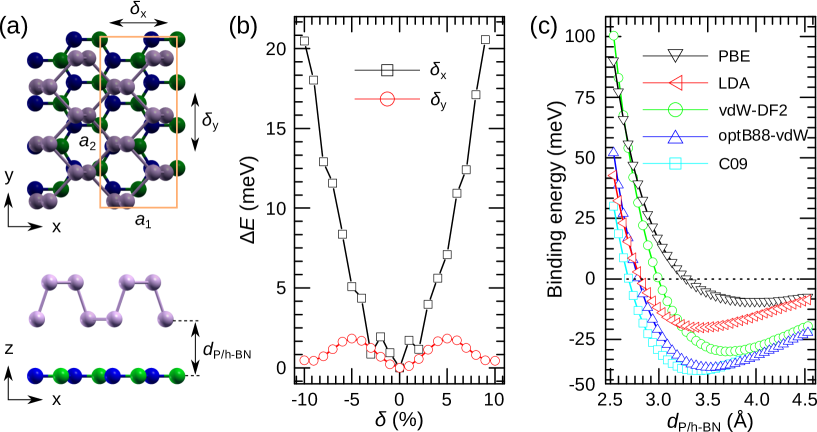
Considering that the lattice parameters of phosphorene and h-BN are different, we construct the heterostructure of P/h-BN by extending h-BN with 14 unit cells to match the fixed phosphorene with 13 unit cells during the geometric optimization, as displayed in Fig. 1(a). In this way, the obtained unit cell of P/h-BN heterostructure has a minimum initial mismatch of 3% fei ; cai2 . It is well known that the stacking manner plays a crucial role in electronic properties of heterostructure. For diminishing this uncertainty in our calculations, we firstly search various stackings of P/h-BN for the most stable one as our starting point. Based on the most stable stacking, we respectively shift phosphorene relative to h-BN along the armchair (x) and zigzag (y) directions. The corresponding energy curves are plotted in Fig. 1(b). As can be seen, when the shift is along the x direction, it needs to overcome a large energy barrier as the puckered structure of phosphorene is involved (see the bottom panel of Fig. 1(a)). By contrast, the energy barrier related to the y-direction shift is quite small. This is because the flat h-BN dominates the energy curve and no obvious change in configuration occurs during this shift process. We also notice that the maximum energy barrier appears at the shift of around 5%, which was not observed in P/graphene heterostructure padilha . At this position, we find that the P atoms of phosphorene are very close to the N atoms of h-BN. Since the residual charges of h-BN largely reside in the N atoms, the Coulomb interactions between the layers are increased, giving rise to a maximum energy barrier.
In order to accurately estimate the interlayer binding of P/h-BN heterostructure, we take five exchange-correlation functionals in our simulations, as shown in Fig. 1(c). Without the vdW correlations, the functionals of PBE and LDA cannot assess rightly the interlayer coupling. The PBE underbinds and increases the interlayer spacing, while the LDA overbinds and reduces the interlayer spacing. Even if the vdW correlation is taken into account, the results are still not converged. The vdW-DF2 method gives an interlayer spacing at least larger than 3.7 Å, leading to a reduced binding energy of around 35 meV. The advanced version of vdW correlation, that is optB88-vdW, seems to be suited for the case of P/h-BN heterostructure. The obtained interlayer spacing is around 3.5 Å and the binding energy is around 44 meV, which are in good agreement with previous calculations rivero ; cai . Based on the same functional of optB88-vdW, the binding energies of bilayer phosphorene and bilayer h-BN are 55 meV cai_sr ; dai and 63 meV hsing , respectively. This means the interlayer vdW interaction between phosphorene and h-BN is weaker than those in both bilayer phosphorene and bilayer h-BN. Such a weak coupling would preserve the electronic properties of phosphorene near the Fermi level in P/h-BN heterostructure. It is also found that this interlayer coupling is comparable to that of P/graphene padilha ; cai . In addition, the vdW functional of C09 produces very similar results to those of optB88-vdW. It is reasonably believed that the optB88-vdW functional can evaluate the interlayer coupling of the heterostructure of P/h-BN at first principle calculation level. And it is thus used for the next calculations. Certainly, more accurate results can be obtained by quantum Monte Carlo method shulenburger , but the computational cost is beyond our tolerance.
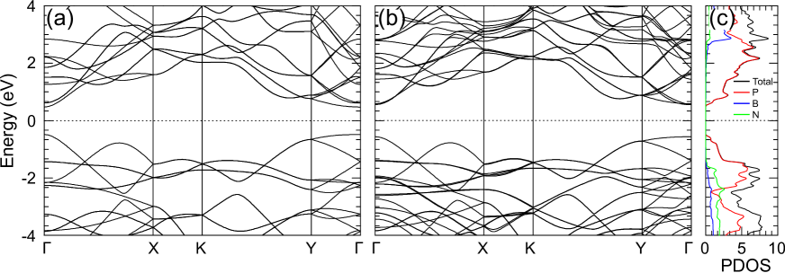
Next, we check whether the P/h-BN heterostructure did inherit the electronic properties of phosphorene. For comparison, the band structure of phosphorene is calculated, as shown in Fig. 2(a). It has a direct band gap of around 0.9 eV at the point. The bands of CBM and VBM have a stronger dependence on the crystal momentum along the -X (armchair) direction than that along the -Y (zigzag) direction. All the electronic properties mentioned above are well in line with previous studies liu ; radi ; qiao . When phosphorene is placed on h-BN substrate, the calculated band structure is displayed in Fig. 2(b). At first glance, the bands near the Fermi level are almost the same as those of phosphorene, which is also verified by the PDOS, as shown in Fig. 2(c). In the energy range from -1.5 eV to 2.0 eV, the P-PDOS does not overlap with the B- and N-PDOS, indicating a very weak coupling between phosphorene and h-BN. A closer look at these two band structures reveals some slight differences. For example, more bands of CBM are degenerate at the point in comparison with phosphorene, resulting from the stacking effect of phosphorene on h-BN substrate. This means that the CBM bands are very sensitive to the external perturbation, in line with previous theory rodin . In P/h-BN heterostructure, since more bands are introduced by the h-BN substrate, the interactions between the bands are enhanced. Such band interactions push the VBM bands of phosphorene closer to each other and make them highly degenerate at the point. As stated by Herring herring , this degeneracy is accidental because bands could degenerate at some specially crystal points perturbed by external stimulation. We also noted that the degeneracy reported by Hu and coauthors hu is smaller than that of our model. This is because the structure of phosphorene is relaxed during the geometry optimization in Hu’s work, which is in contrast to the fixed one in our case. Another effect from the h-BN substrate is the increased band gap of P/h-BN. Wider band-gap h-BN introduces an extra energy of around 0.1 eV into the band gap of P/h-BN heterostructure. Except for the above mentioned two slight differences, the P/h-BN heterostructure almost perfectly inherits the electronic properties of phosphorene near the Fermi level as we expected.
According to the effective-mass theorem ashcroft , the effective mass is associated with the band structure via with being the band energy of the th band at crystal momentum . This means that the effective mass of carriers largely depends on the band curvatures of VBM or CBM. Since the bands near the Fermi level of P/h-BN heterostructure are almost the same as those of phosphorene, their effective masses should be similar. As illustrated in Table I, the introduced h-BN substrate only has an effect on the effective masses along the -Y direction, arising from the enhanced band interactions along this direction. The effective mass for electron decreases from 1.12 in phosphorene to 0.43 in P/h-BN along the -Y direction. The similar trend is also observed in the hole carrier along this direction. By contrast, the effective masses along the -X direction are nearly unchanged, yielding a reduced transport anisotropy compared to phosphorene.
Since the mobility is inversely proportional to the square of deformation potential , the deformation potential is another key factor to act on the carrier mobility, which is in connection with the band structure through with being the energy change of the th band under cell compression or dilatation of and the lattice constant. According to our calculations, though some deformation potentials are influenced by the stacking of h-BN layer, most of the deformation potentials for both electron and hole in P/h-BN are unchanged compared to those of phosphorene (see Table I for more details). Within the framwork of longitudinal acoustic phonon perturbation, the dielectric function is connected to the deformation potential via . According to the analysis suggested by Pollak and coauthors pollak , the main contribution to the is the transitions from the VBM bands to the CBM bands. Thus, the introduced h-BN substrate cannot change the dielectric environment of phosphorene. This is because phosphorene dominates the VBM and CBM bands of P/h-BN, leaving the deformation potentials nearly unchanged. In this perspective, we can easily exclude the enhanced carrier mobility in the P/h-BN heterostructure from the increased damping of Coulombic scattering jena . Unavoidable, two deformation potentials are not unchanged, the deformation potential for electron along x direction is increased 0.8 eV (more than 50%), while that for hole along y direction is decreased 0.3 eV (nearly 60% ). According to the Eq. (1), small deformation potential leads to high carrier mobility. Thus, the electron velocity is suppressed by the h-BN layer, while the hole velocity is accelerated. However, the realization is not that straightforward. As shown in Tab. 1, the electron mobility is higher than that of hole along x direction. Whereas, along y direction, electron mobility loose this advantage. This is because the carrier mobility is not only sensitive to the electronic properties, but also related to the mechanics. In the following, we will demonstrate the power of h-BN substrate on the enhancement of carrier mobility from another viewpoint.
V V. 2D elastic moduli of P/h-BN
As a high- dielectric material, h-BN enters current researches with a main focus on its quantum confinement. For example, other not-flat layered materials can be confined on flat h-BN substrate through vdW stacking, usually appear promising properties such as high carrier mobility vdw_hetero ; bachhuber . By contrast, it is always neglected that its mechanical property also contribute to the ‘high mobility’. In fact, the elastic property of h-BN has a big effect on the charge transport of vdW heterostructures. This is really the case of P/h-BN heterostructure. As shown in Table I, once the substrate of h-BN is introduced, the 2D elastic moduli of P/h-BN are significantly improved: increases from 30 Jm-2 to 320 Jm-2 and from 96 Jm-2 to 370 Jm-2. This directly induces the enhancement of carrier mobility according to Eq. (1). For example, the electron moblity along the x direction is about five times of that of phosphorene. It is also noticed that the carrier mobilities of electron are smaller than those of hole along the y direction, which are in line with the experimental results li . These tell us that the enhanced carrier mobility in the P/h-BN heterostructure is realized via the increased . Why does it happen? We next reveal the underlying mechanism by comparing the 2D elastic moduli of the three materials, i.e., P/h-BN, phosphorene and h-BN.
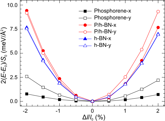
The 2D elastic modulus, i.e., , can be obtained through fitting the expression , where is the total energy and is the equilibrium lattice volume (the xy surface area) for a 2D material. First, we estimate the of phosphorene, as shown in Fig. 3. The strain energy density curve for the x-direction strain is obviously lower than that for the y-direction strain, resulting from the structural anisotropy of phosphorene. The 2D elastic moduli are = 30.24 Jm-2 and = 96.16 Jm-2, in good agreement with previously reported values qiao . Then, we study the 2D elastic moduli of P/h-BN heterostructure. As can be seen in Fig. 3, the strain energy density curves for P/h-BN heterostructure are largely promoted in comparison with phosphorene. Under tension in the range of 0% to 2%, the curve of x-direction is slightly different from that of y-direction. By contrast, this difference disappears under compression. This means that the P/h-BN heterostructre partially preserve the structural anisotropy of phosphorene. Such transport anisotropy only under tension has not been reported in previous literatures. By fitting these curves, two slightly different 2D elastic moduli of = 321.41 Jm-2 and = 369.86 Jm-2 are easily obtained, which are larger than those of phosphorene, but are comparable to those of h-BN. For h-BN, two identical 2D elastic moduli of = 292.34 Jm-2 are obtained, in accordance with experimental and other theoretical reports song ; lee ; kudin . Actually, as shown in Fig. 3, the curves of P/h-BN are roughly the superposition of h-BN and phosphorene, in which h-BN dominates. This means that the P/h-BN heterostructure inherits well the elastic property, that is the 2D elastic modulus, of h-BN, inducing the enhanced carrier mobility in phosphorene. According to our results, further improving the carrier mobility requires a flat substrate which is a 2D layered material itself with higher 2D modulus. Future research can test this prediction.
In pure materials, interactions between the carriers and the acoustical vibrations dominate the mobilities of electrons and holes. The carriers interact only with those acoustical vibrational modes of long wave-length whose properties are determined by the elastic modulus bardeen ; shockley . The acoustical sound velocity in long wave-length limit is connected to the elastic modulus via with being the mass density and the phonon frequency. By stacking phosphorene on h-BN substrate, the 2D elastic moduli are increased by inheriting the elastic property of h-BN, directly increasing the acoustical sound velocity. The corresponding phonon wave-length of P/h-BN is thus decreased, reducing the effective electron-phonon scattering. As a result, the carrier mobilities of P/h-BN are enhanced. This is not surprising. When a soft material is placed on a hard substrate, the lattice vibration of such stacked heterostructure is determined by the hard substrate and is thus suppressed. This demonstrates the underlying mechanism of the enhanced carrier mobility in P/h-BN, which is in contrast to the theory laying emphasis on the increased damping of Coulombic scattering through modifying the dielectric environments jena . At the same time, we also found that the 2D elastic modulus of SiO2 is smaller than those of h-BN. Based on the above discussion, we can infer that the carrier mobilities of phosphorene on h-BN are larger than those on SiO2.
It is known that the h-BN, a substrate, in experiment must be few-layer or even thin film. Thus, we construct a supercell with monolayer phosphorene on top of bilayer h-BN (P/2h-BN) heterostructure. The relative factors are shown in Tab. 1. As it can be seen, the anisotropy inherit from phosphorene becomes weaker, both the electronic and the elastic properties, owing to the isotropic h-BN substrate. However, with the vdW stacking, the carrier mobilities of P/2h-BN heterostructure are not largly improved in both x and y directions as expected. Especially along y direction, the carriers decrease largely compare with P/h-BN but still larger than the monolayer phosphorene. It can be understand that the h-BN layers induce a larger elastic modulus as well as a larger deformation potential. The deformation potential, which is the band energy change during the strain being applied, also play a key roll in carrier mobility calculation. However, comparing with the effect of deformation potential induced by h-BN, the large elastic modulus play a more important role in the carrier mobility of P/2h-BN. The predicted carrier mobilities of bilayer phosphorene on top of monolayer h-BN (2P/h-BN) heterostruture in Tab. 1 also state the similar facts that elastic modulus indeed play a more critical role.
Finally, we should emphasize two points. One is referred to the 2D elastic modulus, which does not increase monotonously with the thickness of substrate. This is because the 2D elastic modulus is indeed related to the deformation potential. Generally speaking, the deformation potential is the energy change of the VBM and CBM during strains being applied, it increases with the vdW stacking, which will suppress the carrier mobility. Another is referred to the predicted carrier mobilities in our work, which are much larger than those reported experimentally. This is mainly caused by the introduction of impurity or/and vacancy during the synthesis process of phosphorene in experiment. We believe the carrier mobility will be largely improved if phosphorene is prepared with high quality nov .
VI VI. Model check
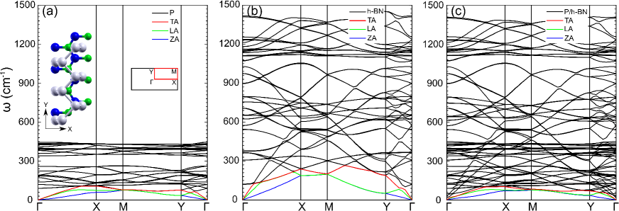
Since the phonon-limited scattering model has its validity limits walu , we calculated phonon spectra of monolayer phosphorene, h-BN, and P/h-BN heterostructure to further validate the accuracy of our methods, as shown in Fig. 4. For more comparable, the supercell are used in calculations. With 12 atoms, phosphorene has 36 vibration branches in its phonon spectra (Fig. 4(a)). The 3 acoustic branches: inplane transverse acoustic (TA, along x direction), the LA (along y direction) mode, and the out-of-plane acoustic (ZA) mode, show linear rise near the point. And a gap of phosphorene vibration (stop band) appears near =300 cm-1, which are in good agreement with previous studies zhu ; jain . Comparing with the phonon vibrations of phosphorene, those of h-BN exhibit higher vibration frequencies (both acoustic modes and optical modes) michel ; jung , as shown in Fig. 4(b). This is because the B-N bonds are shorter in length and stronger in polarity than P-P bonds. The larger slopes of the LA branches near of h-BN indicate the higher speed of sound and the in-plane stiffness. Also, the stop band of h-BN is smaller than that of phosphorene, indicating that h-BN have larger thermal conductivity mcgau . As for P/h-BN heterostructure, it exhibits more vibration modes and smaller stop band comparing with phosphorene, which inherit from h-BN, as shown in Fig. 4(c). That means larger thermal conductivity will also be inherited. Moreover, the acoustic modes of P/h-BN heterostructure are suppression comparing with phosphorene, resulting in larger in-plane stiffness and larger elastic modulus. This can be understand that the out-of-plane vibration modes of phosphorene in P/h-BN are suppressed by the flat h-BN, which reduce the slop of acoustic modes and stop band in heterostructure, leading to a larger carrier mobility.
Conclusions
In conclusion, we have performed first-principles calculations on the P/h-BN heterostructure to reveal the mechanism of the enhaced carrier mobility in phosphorene on h-BN substrate. The enhanced carrier mobility is demonstrated to be correlated with the increased 2D elastic moduli inherited from the h-BN substrate. The unique electronic properties of phosphorene are almost preserved in the P/h-BN heterostructure, which is due to the weak vdW interactions between phosphorene and h-BN. Our results inevitably offer a new perspective to improve the carrier mobilities in phosphorene field effect transistors.
ACKNOWLEDGMENTS
We would like to thank Zhen Zhu (MSU) for valuable communications. This work was supported by the National Basic Research Program of China under Grant No. 2012CB933101 and the National Science Foundation under Grant No. 51372107, No. 11104122 and No. 51202099. This work was also supported by the National Science Foundation for Fostering Talents in Basic Research of the National Natural Science Foundation of China.
∗sims@lzu.edu.cn
References
- (1) X. Ling, H. Wang, S. Huang, F. Xia, and M. S Dresselhaus, PNAS, 112, 4523 (2015); See also references therein.
- (2) H. Liu, A. T. Neal, Z. Zhu, Z. Luo, X. Xu, D. Tománek, and P. D Ye, ACS Nano 8, 4033 (2014).
- (3) B. Radisavljevic, A. Radenovic, J. Brivio, V. Giacometti, and A. Kis, Nat. Nanotech. 6, 147-150 (2011).
- (4) J. Qiao, X. Kong, Z.-X. Hu, F. Yang, and W. Ji, Nat. Commun. 5, 4475 (2014).
- (5) N. Dasgupta, and A. Dasgupta, Semiconductor Devices: Modelling and Technology, ISBN 81-203-2398-X (2004).
- (6) Q. H. Wang, K. Kalantar-Zadeh, A. Kis, J. N. Coleman, and M. S. Strano, Nat. Nanotech. 7, 699-712 (2012).
- (7) C. R. Dean, A. F. Young, I. Meric, C. Lee, L. Wang, S. Sorgenfrei, K. Watanabe, T. Taniguchi, P. Kim, K. L. Shepard, and J. Hone, Nat. Nanotech. 5, 722-726 (2010).
- (8) L. Li, G. J. Ye, V. Tran, R. Fei, G. Chen, H. Wang, J. Wang, K. Watanabe, T. Taniguchi, L. Yang, X. H. Chen, and Y. Zhang, Nat. Nanotech. 10, 608-613 (2015).
- (9) G. Long, S. G. Xu, Z. F. Wu, T. Y. Han, J. X. Z. Lin, J. Y. Shen, Y. Han, W. K. Wong, J. Q. Hou, R. Lortz, and N. Wang, arXiv:1510.06518.
- (10) L. Li, Y. Yu, G. J. Ye, Q. Ge, X. Ou, H. Wu, D. Feng, X. H. Chen, and Y. Zhang, Nat. Nanotech. 9, 372-377 (2014).
- (11) F. Xia, H. Wang, and Y. Jia, Nat. Commun. 5, 4458 (2014).
- (12) D. Jena, and A. Konar, Phys. Rev. Lett. 98, 136805 (2007).
- (13) L. A. Ponomarenko, R. Yang, T. M. Mohiuddin, M. I. Katsnelson, K. S. Novoselov, S. V. Morozov, A. A. Zhukov, F. Schedin, E. W. Hill, and A. K. Geim, Phys. Rev. Lett. 102, 206603 (2009).
- (14) A. Konar, T. Fang, and D. Jena, Phys. Rev. B 82, 115452 (2010).
- (15) E. Artacho, E. Anglada, O. Diéguez, J. D. Gale, A. García, J. Junquera, R. M. Martin, P. Ordejón, J. M. Pruneda, D. Sánchez-Portal, and J. M. Soler, J. Phys.: Condens. Matter 20, 064208 (2008).
- (16) J. P. Perdew, K. Burke, and M. Ernzerhof, Phys. Rev. Lett. 77, 3865 (1996).
- (17) J. Klimes, D. R. Bowler, and A. Michaelides, J. Phys.: Condens. Matter 22, 022201 (2010).
- (18) D. M. Ceperley, and B. J. Alder, Phys. Rev. Lett. 45, 566-569 (1980).
- (19) K. Lee, E. D. Murray, L. Kong, B. I. Lundqvist, and D. C. Langreth, Phys. Rev. B 82, 081101 (2010).
- (20) V. R. Cooper, Phys. Rev. B 81, 161104 (2010).
- (21) J. Isberg, J. Hammersberg, E. Johansson, T. Wikström, D. J. Twitchen, A. J. Whitehead, S. E. Coe, and G. A. Scarsbrook, Science 297, 1670 (2002).
- (22) E. H. Hwang, and S. Sarma, Phys. Rev. B 77, 115449 (2008).
- (23) S. Takagi, A. Toriumi, M. Iwase, and H. Tango, IEEE Trans. Electron Devices 41, 2363 (1994).
- (24) S. Bruzzone, and G. Fiori, Appl. Phys. Lett. 99, 222108 (2011).
- (25) Z. Zhang, J. Xie, D. Yang, Y. Wang, M. Si, and D. Xue, Appl. Phys. Express 8, 055201 (2015).
- (26) Z. Yu, Z. -Y. Ong, Y. Pan, Y. Cui, R. Xin, Y. Shi, B. Wang, Y. Wu, T. Chen, Y. -W. Zhang, G. Zhang, and X. Wang, Advanced Materials 28, 547-552 (2016)
- (27) R. Fei, and L. Yang, Appl. Phys. Lett. 105, 083120 (2014).
- (28) Y. Cai, Q. Ke, G. Zhang, Y. P. Feng, V. B. Shenoy, and Y.-W. Zhang, Adv. Funct. Mater 25, 2230-2236 (2015)
- (29) J. E. Padilha, A. Fazzio, and A. J. R. da Silva, Phys. Rev. Lett. 114, 066803 (2015).
- (30) P. Rivero, C. M. Horvath, Z. Zhu, J. Guan, D. Tománek, and S. Barraza-Lopez, Phys. Rev. B 91, 115413 (2015).
- (31) Y. Cai, G. Zhang, and Y.-W. Zhang, J. Phys. Chem. C 119, 13929 (2015).
- (32) Y. Cai, G. Zhang, and Y.-W. Zhang, Sci. Rep. 4, 6677 (2014).
- (33) J. Dai, and X. C. Zeng, J. Phys. Chem. Lett. 5, 1289 (2014).
- (34) C.-R. Hsing, C. Cheng, J.-P. Chou, C.-M. Chang, and C.-M. Wei, N. J. Phys. 16, 113015 (2014).
- (35) L. Shulenburger, A. D. Baczewski, Z. Zhu, J. Guan, and D. Tománek, arXiv:1508.04788v1.
- (36) A. S. Rodin, A. Carvalho, and A. H. Castro Neto, Phys. Rev. Lett. 112, 176801 (2014).
- (37) C. Herring, Phys. Rev. 52, 365-373 (1937).
- (38) T. Hu, and J. Hong, ACS Appl. Mater. Interfaces 7, 23489-23495 (2015).
- (39) N. W. Ashcroft, and N. D. Mermin, Solid State Physics (Saunders College, Philadelphia, 1976).
- (40) F. H. Pollak, M. Cardona, C. W. Higginbotham, F. Herman, and J. P. Van Dyke, Phys. Rev. B 2, 352 (1970).
- (41) A. K. Geim, and I. V. Grigorieva, Nature 499, 419 (2013).
- (42) F. Bachhuber, J. von Appen, R. Dronskowski, P. Schmidt, T. Nilges, A. Pfitzner, and R. Weihrich, Angew. Chem. Int. Ed. 53, 11629 (2014).
- (43) L. Song, L. Ci, H. Lu, P. B. Sorokin, C. Jin, J. Ni, A. G. Kvashnin, D. G. Kvashnin, J. Lou, B. I. Yakobson, and P. M. Ajayan, Nano Lett. 10, 3209 (2010).
- (44) C. Lee, X. Wei, W. J. Kysar, and J. Hone, Science 321, 385 (2008).
- (45) K. N. Kudin, G. E. Scuseria, and B. I. Yakobson, Phys. Rev. B 64, 235406 (2001).
- (46) J. Bardeen, and W. Shockley, Phys. Rev. 80, 72 (1950).
- (47) W. Shockley, and J. Bardeen, Phys. Rev. 77, 407 (1950).
- (48) K. S. Novosolov, V. I. Fal’ko, L. Colombo, P. R. Gellert, M. G. Schwab, and K. Kim, Nature 490, 192-200 (2012).
- (49) W. Walukiewicz, H. Ruda, J. Lagowski, and H. Gatos, Phys. Rev. B 30, 4571-4582 (1984).
- (50) Z. Zhu, and D. Tománek, Phys. Rev. Lett. 112, 176802 (2014).
- (51) A. Jain, and Alan J. H. McGaughey, Sci. Rep. 5, 08501 (2015).
- (52) K. H. Michel, and B. Verberck, Phys. Rev. B 83, 115328 (2011).
- (53) S. Jung, M. Park, J. Park, T.-Y. Jeong, H.-J. Kim, K. Watanabe, T. Taniguchi, D. H. Ha, C. Hwang, and Y.-S. Kim, Sci. Rep. 5, 16642 (2015)
- (54) A. J. H. McGaughey, and M. I. Hussein, Phys. Rev. B 74, 104304 (2006).
| Material | type | ||||||||
|---|---|---|---|---|---|---|---|---|---|
| P/h-BN | e | 0.21 | 0.43 | 321.41 | 369.86 | 2.21 | 6.58 | 22.34 | 1.42 |
| h | 0.18 | 2.99 | 321.41 | 369.86 | 2.83 | 0.24 | 6.53 | 59.96 | |
| phosphorene | e | 0.16 | 1.31 | 30.24 | 96.16 | 1.49 | 6.01 | 4.00 | 0.09 |
| h | 0.15 | 3.28 | 30.24 | 96.16 | 2.80 | 0.58 | 0.79 | 2.67 | |
| P/2h-BN | e | 0.20 | 0.67 | 555.52 | 648.00 | 2.09 | 6.71 | 37.32 | 1.26 |
| h | 0.18 | 3.74 | 555.52 | 648.00 | 2.71 | 0.71 | 11.00 | 9.00 | |
| 2P/h-BN | e | 0.22 | 0.31 | 357.29 | 466.41 | 3.68 | 6.64 | 8.57 | 2.44 |
| h | 0.18 | 1.78 | 357.29 | 466.41 | 2.73 | 1.37 | 7.80 | 4.09 |