Anisotropic transport of normal metal-barrier-normal metal junctions in monolayer phosphorene
Abstract
We study transport properties of a phosphorene monolayer in the presence of single and multiple potential barriers of height and width , using both continuum and microscopic lattice models, and show that the nature of electron transport along its armchair edge ( direction) is qualitatively different from its counterpart in both conventional two-dimensional electron gas with Schrödinger-like quasiparticles and graphene or surfaces of topological insulators hosting massless Dirac quasiparticles. We show that the transport, mediated by massive Dirac electrons, allows one to achieve collimated quasiparticle motion along and thus makes monolayer phosphorene an ideal experimental platform for studying Klein paradox. We study the dependence of the tunneling conductance as a function of and , and demonstrate that for a given applied voltage its behavior changes from oscillatory to decaying function of for a range of with finite non-zero upper and lower bounds, and provide analytical expression for these bounds within which decays with . We contrast such behavior of with that of massless Dirac electrons in graphene and also with that along the zigzag edge ( direction) in phosphorene where the quasiparticles obey an effective Schrödinger equation at low energy. We also study transport through multiple barriers along and demonstrate that these properties hold for transport through multiple barrier as well. Finally, we suggest concrete experiments which may verify our theoretical predictions.
I Introduction
Two dimensional crystals composed of single or few atomic layers are the focus of intense research currently, on account of their remarkable optical, electronic and mechanical properties. Moreover such materials, as shown in recent years revgr1 ; revti1 , serve as test bed for Dirac physics. This property of these materials arises from the fact that their low-energy quasiparticles obey an effective Dirac-like equation. Such quasiparticles lead to a host of unconventional thermodynamic and transport properties. Examples of such unconventional properties seen in the context of graphene and topological insulators include unconventional quantum Hall effect hallref1 , unusual Kondo effect kondoref1 , and unconventional transport properties transref1 ; transref2 . Indeed, the latter property serves as one of the key aspects of Dirac (relativistic) materials which distinguishes them from conventional materials whose quasiparticles obey Schrödinger equation. For example, the former class of materials display oscillatory behavior of the transmission through a potential barrier as a function of the barrier height or width; this behavior is in complete contrast to an exponentially decaying transmission function found for the latter class History_klein ; Klein_nature ; Robinson .
Phosphorene ph-1 ; ph-review is another such Dirac material which is being actively investigated for electronic and other applications ph-tr1 ; ph-tr2 ; ph-tr3 on account of its anisotropic electronic ph-bs1-dft , thermal ph-thermal1 ; ph-thermal2 and optical properties ph-bs1-dft . A hallmark of monolayer phosphorene is its anisotropic band-structure, which displays an almost flat parabolic Schrödinger like dispersion along the zigzag edge ( direction) and a predominantly Dirac like dispersion along the armchair edge ( direction)ph-bs1-dft ; ph-bs2-tb ; ph-bs2-tb-2 ; Doh ; ph-bs3-kp ; ph-bs3-tb ; ph-bs4-tb . Such anisotropic bandstructure distinguishes phosphorene from other Dirac materials such as graphene or topological insulator surface where the effective Dirac theory is massless and isotropic. Accordingly, the transport properties across single or multiple potential barriers in phosphorene are expected to be different depending on the orientation of the barrier relative to the plane. The anisotropy of the low energy dispersion in phosphorene thus offers an opportunity to simultaneously probe the relativistic as well as the non-relativistic nature of electrons in a transport experiment based on a normal-barrier-normal (NBN) junctions. Depending on the orientation of the phosphorene monolayer with respect to the measuring electrodes, it is expected to display an oscillatory behavior in the transmission function as a function of the barrier strength as well as the barrier height along the armchair direction, and an exponential decaying transmission function along the zigzag direction. However, a detailed theoretical investigation of such properties has not been yet carried out.
It is the aim of this paper to highlight these anisotropic transport signatures of phosphorene across a NBN junction with different orientations. More specifically, we study the transport properties of quasiparticles in monolayer phosphorene in the presence of single and multiple potential barriers oriented along (subsequently referred to as the direction). The main results that we obtain from such a study are as follows. First, we show that the transport shows several signatures consistent with a gapped Dirac quasiparticle; this is in sharp contrast to the case when the barrier is along ( direction) for which the transport properties conform to those due to Schröndinger quasiparticle. Second, we show that for a barrier along the direction, the dominant contribution to the transport comes from the quasiparticles which impinge on the barrier at near-normal incidence provided the applied voltage is close to the bottom of the conduction band, leading to collimated transport of electrons. The degree of such collimation can be tuned by the external applied voltage . Third, we find that this property, which is experimentally inaccessible in gapless Dirac materials such as graphene and topological insulators, allows us to tune to a regime where the conductance mimics the behavior of normal transmission amplitude. This leads to the possibility of observing signature of Klein paradox through measurement of . Fourth, we find that both the normal transmission and displays oscillatory or decaying behavior as a function of the barrier width depending on the relative strength of the dimensionless barrier potential and the applied voltage , where is the mass gap; the behavior of and changes from oscillatory to a monotonically decreasing function of for . We also show analytically that and for using a continuum approximation to the lattice model of phosphorene and demonstrate that the phenomenon described above persists beyond the continuum approximation used to obtain the expression of and . We point out that such transport behavior is qualitatively different from their counterparts in both conventional Schrödinger and gapless Dirac materials. Fifth, we study transport of phosphorene quasiparticles through multiple barriers (each of height and width ) along and demonstrate that all of the above-mentioned features derived for transport through a single barrier holds in the multiple barrier case. The main difference between the two manifests itself in additional peaks in normal transmission or conductance as a function of in the oscillatory regime () for the multiple barrier case; we provide an analytical explanation for this phenomenon for barriers. Finally, we discuss experiments which can test our theory.
The manuscript is organized as follows. In Sec. II, we outline the band structure of phosphorene and chart out the continuum Hamiltonian used for transport calculation. Such calculations for the single potential barrier along is discussed in Sec. III, while transport through multiple barriers along is discussed in Sec. IV. Finally, we discuss our results, chart out possible experiments which can test them, and conclude in Sec. V.
II Low energy effective Hamiltonian of Phosphorene
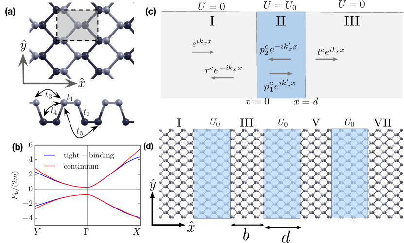
The band-structure of monolayer phosphorene, is well known from ab-initio calculations ph-bs1-dft ; ph-bs2-tb , and it has been used to construct effective low energy Hamiltonian using several approaches such as method ph-bs3-kp , the tight-binding approach ph-bs2-tb ; ph-bs2-tb-2 ; ph-bs3-tb ; ph-bs4-tb ; Doh , and the methods of invariants ph-bs-inv1 . All of these methods yield qualitatively similar band structure. Thus for this paper we use the two band Hamiltonian which is obtained from the four band tight-binding Hamiltonian on a discrete lattice, making use of the symmetry ph-bs3-tb and expanding around the point. The origin of such symmetry can be understood in the following manner. The unit cell of phosphorene, shown in Fig. 1(a), contains four phosphorus atoms, such that the upper and the lower layers each contain two of these atoms. This leads to the point group invariance which constitutes invariance under a shift along the plane of the layer combined with exchange of the layer indices. It is therefore sufficient to consider a reduced unit cell of two atoms either in the upper or in the lower layer since the transfer energy of atoms in these layers are identical.
Our starting point is the effective two-band tight-binding model based on Refs. [ph-bs2-tb, ; ph-bs3-tb, ]. This tight-binding model is given by
| (1) |
where the summation runs over the lattice sites, is the hopping matrix element between and sites, and is the annihilation operator of an electrons at site . The corresponding two-band Hamiltonian can be written in momentum space as ph-bs3-tb
| (2) | |||||
where for are the different transfer matrix elements indicated in Fig. 1(a) with eV, eV, eV, eV and eV, are the Pauli matrices in the band basis, is the two component fermion field with being the annihilation operators corresponding to electrons of the two phosphorene atoms from the unit cell, denotes the identity matrix, and we have scaled wavevectors by the corresponding lattice lengths and . The energy spectrum of this Hamiltonian is given by
| (3) |
where the sign in the subscript indicates conduction (valence) band. A plot of these bands as a function of (for ) and (for ) is shown in Fig. 1(b). The corresponding eigenvectors are given by
| (4) |
where and denotes the signum function.
The Hamiltonian may be simplified in the low-energy low-momentum or continuum limit. Using the identities and , one can obtain the continuum version of Eq. (II): , to be
| (5) |
where is the chemical potential, and , with eV. The other parameters in Eq. (5), can be expressed in terms of in a straightforward manner and are givenph-bs3-tb by eV, eV, eV, and eV. Here we note that which allows one to have an approximately linear dispersion in for small . The eigenvalues and eigenfunctions of are given by
| (6) | |||||
and . From Fig. 1(b), we find that the energy bands of the continuum model match with those of the lattice model. We note that in the continuum limit, since , the Hamiltonian is linear (Dirac like) in but parabolic (Schrödinger like) in ; consequently, the nature of the quasiparticle transport and the effect of a potential barrier depends crucially on the its orientation in the plane. We shall discuss this phenomenon in detail in the next section.
III Transport across a single barrier: NBN junction
In this section, we present an analysis of transport across a single barrier. We first present the general formalism for both the lattice model (Eq. (II)) and its continuum approximation (Eq. (5)) in Sec. III.1. The numerical results of the analysis of the formalism developed in Sec. III.1 is presented in Sec. III.2.
III.1 Formalism
In this section, we study ballistic transport in phosphorene monolayer in the presence of a single barrier of strength and width as shown in Fig. 1(c). We will primarily be focussed on transport in the direction, which is likely to have signatures of Dirac quasiparticles.
Let us first discuss the formalism for calculating transmission and conductance along using the two band lattice Hamiltonian of Eq. (II). The wave function for the particles with transverse momenta and energy (which we choose to lie in the conduction band), where is the chemical potential and is the applied bias voltage, moving along direction can be obtained by diagonalization of Eq. (II). The corresponding eigenfunctions can be read off from Eq. (4); for an electron moving along (right (+) and left (-) moving electrons) with momenta , it is given by with
| (9) |
where and is obtained from the solution of
| (10) |
We first note that the sign here in the superscript indicates right(left) moving electrons in contrast to those in the subscript in Sec. II which indicated conduction and valence band energies. Since for transport we shall focus only on electrons in the conduction band in region I, we omit the subscript indicating conduction or valence band for brevity. We also note that Eq. (10) admits two solution for corresponding to any given energy and transverse momentum . One of these solutions is real and represents a propagating wave while the other is imaginary and represents an evanescent wave. While the expectation of the current operator and hence the conductance receives contribution from the propagating wave, the formalism that we use requires that the evanescent wave solutions are treated at an equal footing. In what follows, we denote the solutions, obtained by numerical solution of Eq. (10), as and with . In terms of these wavevectors, one can write the wavefunction in region I (which extends in the region as seen in Fig. 1(c)) as
| (18) | |||||
where , , and is obtained using Eq. (4). In Eq. (18) we have kept only the decaying evanescent modes, and and denotes reflection coefficients corresponding to the propagating and the evanescent modes respectively.
The wavefunction in region II (as shown in Fig. 1(c)) consists of left and right propagating modes as well as evanescent waves which decays and grows within . Here depending on the magnitude of the applied barrier potential and , the longitudinal wavevector may be obtained from either the valence or the conduction band energy expressions (Eq. 3). This is in contrast to the situation in regions I and III where they are necessarily obtained using energy expressions for the conduction band. The longitudinal wavevector for these modes are obtained from the solution of
| (19) |
and we denote these wavevectors as and . In terms of these, one can write the wavefunction in region II as
| (29) | |||||
where , , , and . In Eq. (LABEL:wav2), and are coefficients corresponding to the left and the right propagating mode, and and are the coefficients corresponding to decaying and growing evanescent mode. Note that since region II extends within a finite span of , the solution with the growing evanescent mode is admissible in this region.
Finally, we consider the wavefunction in region III which extends for . In this region, one finds
| (35) |
where , and are the transmission amplitude corresponding to the propagating and the evanescent mode. Note that in this region, similar to region I, only the decaying evanescent mode is admissible.
To obtain the reflection and transmission coefficients, we use the standard procedure of imposing the continuity condition for the wavefunction as well as the current at and . This leads to the conditions
| (37) |
where the velocity operator can be obtained using Eq. (II) and is given by
| (38) | |||||
with the substitution . Substituting Eqs. (18)-(LABEL:wav3) in Eq. (37), we can then obtain the following eight equations,
| (39) | |||
where and the quantities and are defined as
| (40) |
Here can assume values depending on values of : or , takes values of or depending on or , and we have suppressed the and energy dependence of and for clarity. Note that the presence of the evanescent waves (complex solutions for ) is essential for unique solution of Eq. (39); without them, we would have an overdetermined set of equations.
Equation (39) is solved numerically to obtain the reflection and the transmission coefficients and . The transmission probability can be computed in terms of these as . Note that which corresponds to the transmission amplitude of the evanescent mode decays exponentially in region III away from the barrier and hence it does not contribute to the transmission for , where is the system size and the lead is placed at . To compute the conductance in the presence of a single barrier we first note that the current operator along is given by and thus the current flowing in regions I and III are given by
| (41) |
The conductance of the system can then be computed as
| (42) |
where , and denotes the maximum transverse momenta for which Eq. (6) admits a real solution for and the limits of integration are decided by the fact that the dispersion in Eq. (3) is symmetric in .
Having described the formalism to calculate the transmission and conductance for the two band lattice Hamiltonian, we now focus our attention on the low energy and small momentum limit, for which the system is described by . In what follows we shall neglect the term in the expression of ; this is justified by the fact that for low momenta and so thats the dependence of may be neglected. The motivation for solving the problem within this approximation is two-fold. First, as we shall see, the conductance and transmission coefficients computed within this approximation matches those from the exact lattice model at low applied voltages and second, this approximation yields an analytic expression for the transmission coefficient which allow further insight into the transport properties of the system.
For electrons described by Eq. (5) with , let us consider a wave incident on the barrier with energy and transverse wavevector . The wavefunction of the electron can be computed using Eqs. (5)-(6) as , where , and is given by
| (43) |
The reflected wavefunction in this case is given by . Thus the wave function in region I (see Fig. 1(c)) can be written as
| (44) |
We note that the continuum approximation does not support the evanescent modes found in the lattice formulation. This feature is consistent with the fact that for the effective Dirac-like Hamiltonian with linear dispersion that we found within this approximation, we only need continuity of the wavefunctions at the barrier edges ( and ); the continuity of the derivative of the wavefunction is no longer necessary since we are dealing with linear differential operators along . This situation is in contrast to Schrödinger electrons for which both the wavefunction and its derivative needs to be continuous across the barrier transref1 ; transref2 .
In the barrier region, the wavefunction can be expressed as
| (50) | |||||
where , and is given by
| (51) |
Finally, in region III, the transmitted electron wavefunction is given by
| (54) |
The reflection and the transmission coefficients can be determined using standard procedure of demanding wavefunction continuity at the interfaces at and : and . This yields
| (55) | |||
A solution of Eq. (III.1) leads to the transmission and reflection amplitudes within the continuum approximation,
| (56) |
where and . The transmission probability is then given by
| (57) |
The conductance may then be obtained using
| (58) |
Note that Eq. (58) is a simplified version of Eq. (42), for the case when the incoming and the outgoing regions across the barrier are identical. We shall analyze the results obtained from the formalism developed in this section for both the lattice model and its continuum approximation in Sec. III.2.
Before ending this section, we analyze Eq. (57) in the thin barrier limit where and with a fixed ratio , and . In this limit, Eq. (57) may be further simplified to obtain
| (59) |
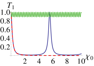
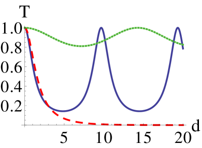
Equation (59) can be analyzed to obtain several characteristics of the transmission coefficient . We first note that as (which means ) and , which reproduces Klein paradox result for massless Dirac fermions seen in graphene. Second for , , and consequently as a function of the effective barrier strength oscillates with a frequency as or is varied; thus knowing and , one can estimate the mass of single-layer phosphorene by measuring the frequency of such oscillation. Third, for as is tuned such that , where
| (60) |
becomes imaginary and hence changes from being oscillatory to a decaying function of . For , we find that
| (61) |
Such a qualitative change in , which is generally not seen in other massless Dirac materials, may serve as an accurate measurement of the mass gap in phosphorene. It is to be noted that while indicates that the applied voltage is larger than the barrier height which is expected to lead to non-decaying behavior of (and hence ) with , the oscillatory behavior of for is a property of Dirac nature of the phosphorene electrons. The difference of such transport from that in graphene follows from the decaying behavior of for ; such a behavior is absent for transport in graphene and topological insulators where and are oscillatory functions of for any . We find that this property is not a consequence of the thin barrier limit can also be seen from Eqs. (57) and (51). Clearly the decaying behavior arises only when the wavevector in the potential region, is imaginary. Fourth, we note that the contribution to the transmission modes comes from transverse momenta modes for which away from the barrier. This requires the condition , where we have set the chemical potential so that corresponds to the bottom of the conduction band. Thus by tuning the applied voltage one may reach a regime where the conductance
| (62) |
receives its contribution only from the quasi particles with near normal incidence. This leads to collimated transport; furthermore since the dependence of in this regime is negligible, the oscillation frequency of with the barrier width would mimic that of . This enables us to realize a setup where Klein paradox could be realized via measurement of ; we note that it is impossible to reach this regime in gapless Dirac systems such as graphene. We shall study the feasibility of this proposition in details in the next section. Finally, we note that in contrast to graphene, the presence of a finite mass gap allows us to tune transmission through the barrier. This can be seen by inspecting Eq. (51); we find that there are no propagating modes inside the barrier, for . The key point is that the value of can tuned to zero by choosing which allows one to tune, particularly for large , transmission through the barrier by tuning .
III.2 Results
In this subsection, we shall chart out the results corresponding to the theory of transport of monolayer phosphorene electrons through a single barrier along the direction developed in Sec. III.1. We shall first analyze the results for the continuum model (Eq. (II)) and then compare its prediction with those obtained from the lattice model (Eq. (5)).
To this end, we first plot the normal transmission as a function of the barrier width for several representative values of (barrier height) for fixed (incoming energy) as shown in Fig. 2. We note that for (or alternately ), displays oscillatory behavior with increasing which is similar to that of massless Dirac-like electrons as seen in graphene Klein_nature and in contrast to that of conventional Schrödinger electrons with parabolic dispersion for which the transmission probability decreases monotonically with . However, in contrast to graphene, shows a decaying behavior as a function of for [or alternately for ; (Eq. (60))]. As is further decreased below (or ), becomes an oscillatory function of with frequency given by (green dashed plot in the left panel of Fig. 2). A similar behavior is seen for (Eq. 57) as shown in the right panel of Fig. 2. We note that this leads to tunability of transmission which is a result of both the band structure of phosphorene and the presence of the mass gap ; such behavior is therefore absent in graphene.
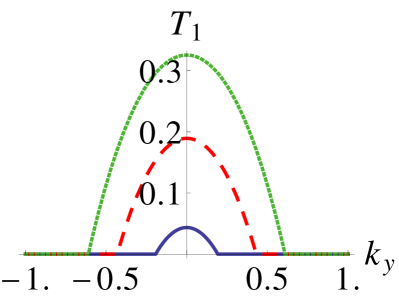
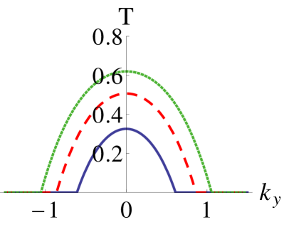
Next, we plot as a function of for a fixed , , and for several representative values of as shown in the left panel of Fig. 3. As we discussed in the last section, the transport becomes increasingly collimated as the applied voltage is tuned towards the bottom of the conduction band (which in our notation corresponds to ) since lesser number of modes satisfies Eq. (43) for real values of . This feature, which holds beyond thin barrier limit as shown from the plot of (Eq. 57) in the right panel of Fig. 3, can be shown to be related to the relative flatness of phosphorene bands near the band bottom along the -direction in contrast to that in the -direction; this naturally leads to collimated behavior. Thus, at sufficiently low , dominates the conductance as shown in the left panel of Fig. 4. At low , the oscillatory behavior of as a function of , which is a signature of Klein paradox for gapped Dirac systems Klein_nature , may therefore be observed via measurement of tunneling conductance . We note that such a measurement would be impossible in graphene since one needs to be very close to the Dirac point to observe this phenomenon where the density of state is extremely small. Such an equivalence between and (Eq. 57) is lost for larger as shown in the right panel of Fig. 4.
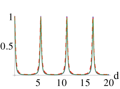
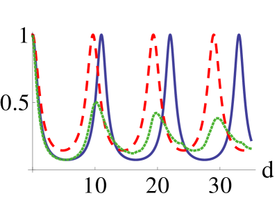
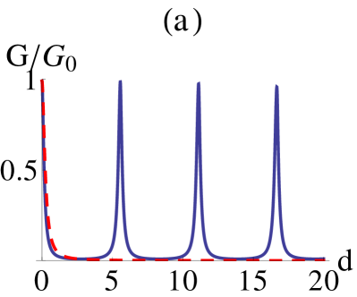
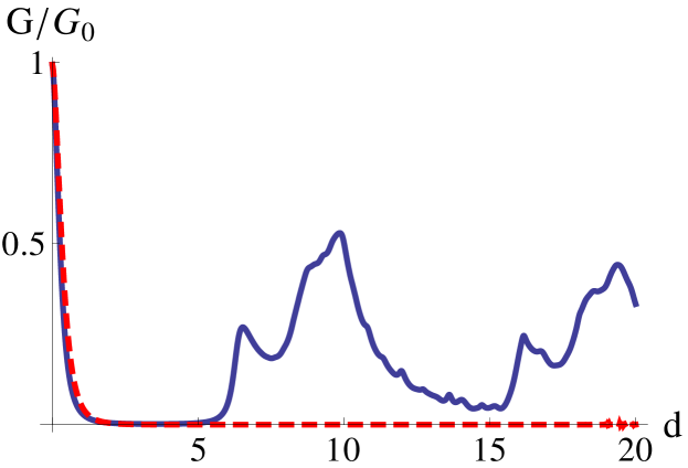
Next, we plot the dimensionless conductance as a function of the barrier width in Fig. 5(a). We find that (top left panel) for small , , which mimics the behavior of , shows oscillatory behavior for ; the period of these oscillations are determined by . For smaller , decays with barrier strength; thus one can effectively tune the conductance of phosphorene by tuning the strength of potential barriers along , provided that the applied voltage stays small. For larger , the behavior of deviates from that of since a large number of modes contribute to the transmission; in this regime (Eq. 58) never reaches its maximal value of unity. This feature is shown in Fig. 5(b); however, we note that still remains an oscillatory or decaying function of depending on the value of . The bottom panel of Fig. 5 displays the behavior of as a function of the applied voltage (left panel) for fixed barrier potential and barrier width and as a function of for fixed and (right panel). For the former plot, in Fig. 5(c), is initially an increasing function of followed by a decaying behavior for while for , it stays close to zero for all . This can be understood from the fact that is an increasing function of . If , as (and thus ) increases and crosses , the behavior of changes from oscillatory to decaying as a function of . This is reflected by an initial increase in as a function of followed by a decaying behavior for . However, if , is always small and remains close to zero for any ; this happens for as shown in Fig. 5(c) (red dashed line). For the latter plot, in Fig. 5(d), we find that decreases as a function of for a fixed for ; however, as is increased to values larger than , becomes an oscillatory function of . This behavior can be easily understood from Eq. (57) noting that and therefore is an oscillatory or decaying function of depending on whether is real of imaginary. Since becomes imaginary for , becomes a decaying function of within this range. For , oscillates with ; thus we find that changes from being oscillatory to decaying to oscillatory function of with increasing .
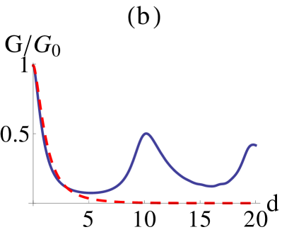
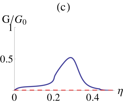
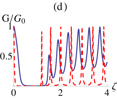
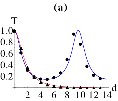
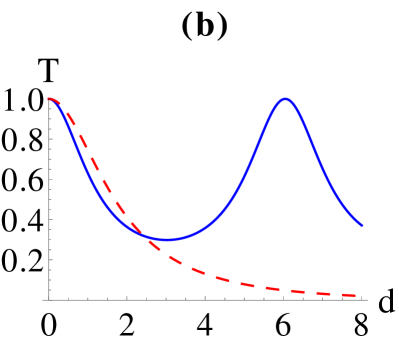
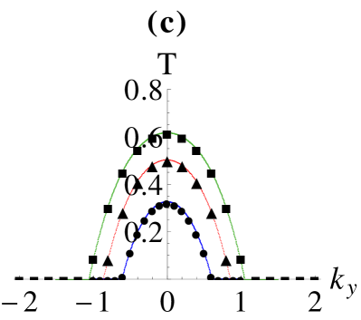
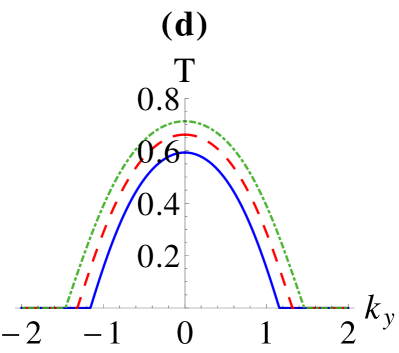
Next, we compare the continuum results obtained with those obtained from the lattice Hamiltonian (Eq. (II)) using Eqs. (39) and (42). A plot of the normal transmission as a function of obtained from the lattice model is compared to those obtained from the continuum model in Fig. 6(a); we find that the plots agree quite well to the results of the continuum model for small . For larger , where the continuum model is expected to fail, the results of the lattice model, shown in Fig. 6(b), shows the expected oscillatory (and decaying) behavior of with for . Thus we demonstrate that the change from oscillatory to decaying behavior of transmission with found in the continuum model holds at larger applied voltages where the lattice model provides an accurate description of the transport. The plot of as a function of the transverse momentum , shown in Fig. 6(c), reproduces the expected collimated nature of the transmission; moreover, it agrees quite well with the results obtained form the continuum model. This highlights the fact that as long as is small, the results of the lattice and the continuum models agree with each other; this provides the justification of our continuum analysis which provides a better analytic insight for the obtained results. In Fig. 6(d), we show the nature of dependence of for larger applied voltages, , for which the continuum model is not expected to be accurate.
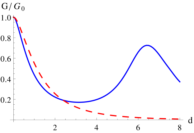
Finally, we note that the oscillatory/decaying behavior of as a function of can also be found in , as calculated from the lattice model, for . This is shown in Fig. 7; we find that displays oscillatory (decaying) behavior as a function of for (). This demonstrates that the switch from oscillatory to decaying behavior, evident from the continuum model valid for small applied voltages, also persists for a larger ranges of applied voltages where the continuum model is not expected to be accurate; this property is therefore more general, and not a consequence of the continuum approximation used earlier in this section. This property stems from the longitudinal wavevector in the barrier switching from real to imaginary which occurs for both the lattice and the continuum model.
Having studied the transport across a barrier oriented along the (armchair) direction, we now compare the transmission for a single barrier along (zigzag) direction with height and width . The details of computing the transmission is analogous to the procedure outlined in Sec. III.1 for the lattice model with the difference that now plays the role of transverse momentum. The result of this analysis is shown in Fig. 8. We find that in contrast to the transmission along , displays decaying behavior as a function of for all as expected for transport mediated by Schrödinger quasiparticles with a parabolic dispersion. This difference originates from the anisotropic band structure of phosphorene and highlights the importance of the orientation of the barrier which controls the qualitative nature of transport in this material.
IV Multiple NBN junctions
In this section, we shall extend the formalism developed in Sec. III.1 to treat the case of multiple potential barriers along . The proposed experimental setup is sketched in Fig. 1(d). We shall consider the case where all the barriers have a height and width ; the distance between two successive barriers is denoted by . In what follows, we are going to use the continuum approximation discussed in Sec. II so that the system Hamiltonian is given by Eq. (5).
To calculate the transmission across multiple barriers, we use the transfer matrix formalism which has been developed for gapless Dirac electrons on the surface of a topological insulator in Ref. [smondal1, ]. The first step in developing this formalism constitutes obtaining an expression for the wavefunction in the region (i.e. region between and barriers), where is an integer. Recall that the barrier regions are labeled by even integers in Fig. 1(d). The quasiparticle wave function in different regions are given by , and is given by smondal1
| (63) | |||||
Here the coefficients are given by and the matrices and are given by
| (64) |
and is obtained from by replacing with along with .
Next, we employ the boundary conditions at the junctions by imposing continuity of the wavefunctions across the barrier. This leads to, after some algebra, the expressions for the reflection () and transmission () coefficients across the barriers. The reflection and the transmission coefficients can be expressed in terms of the elements of the transfer matrix as
| (65) |
where (for a system with n barriers) is defined via the relation . It can be evaluated to be
| (66) | |||||
where and the elements of the matrix are explicitly given by
| (69) | |||||
| (70) |
and and are defined in Eq. (43) and Eq. (51), respectively. The transmission coefficient and the conductance across the barrier can be obtained as and .
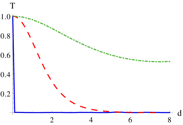
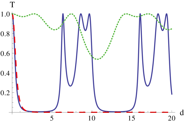
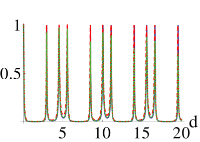
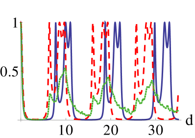
To explore the impact of multiple barriers, we first plot the normal transmission for low applied voltage as a function of for barriers in Fig. 9. We find that similar to the behavior of for the single barrier case, for multiple barriers, is either a decaying or an oscillatory function of depending on the value of . The only quantitative difference that we find are as follows. First, the structure of the oscillations for or becomes more complicated due to the presence of multiple barriers and second the decay of , for becomes much sharper. Next, we compare the behavior of conductance with that of for several representative values of in Fig. 10. We note that as in the case of single barrier, mimics for small (left panel of Fig. 10); for larger values of , and shows different behavior. This indicates collimated transport for small across multiple barriers, which is also expected from our results in Sec. III.2. Finally, we plot the conductance as a function of for and two representative values of in Fig. 11. We find that for , shows a sharp decay as a function of while it shows oscillatory behavior for .
The nature of the oscillations of transmission or conductance can be understood analytically by considering the simplest case of multiple barriers corresponding to . In this case, some straightforward algebra, starting from Eqs. (64), (66), and (70), yields an analytic expression of as
| (71) | |||||
where is the transmission through a single barrier. From Eq. (71), it is easy to see that for (i.e for , where is an integer) and also for leading to two distinct peaks of the transmission. The number of such peaks increase with ; thus the oscillation pattern becomes more complicated with increasing . We also note that the behavior of as a function of is controlled by ; hence the oscillatory or decaying nature of the transmission and conductance, across multiple barriers, is also controlled by whether becomes real of imaginary for a given , and .
V Discussion
In this work, we have studied transport through a single as well as multiple barriers in phosphorene along the armchair edge (-direction) and have shown that such transport have features which are qualitatively distinct from their counterparts for both conventional Schrödinger materials and gapless Dirac systems such as graphene and topological insulator surfaces. We have also shown that due to the anisotropic band structure in phosphorene, such unconventional properties are expected only for barriers along ; for barriers along , the transport displays standard Schrödinger behavior.
The key unconventional features that our study unravel are as follows. First, we show that the band structure of phosphorene allows near normal transmission to dominate the conductance as the applied voltage is tuned to near the bottom of the conduction band. Consequently one obtains progressively collimated transport as approaches the band bottom. Second, in the limit where the applied voltage is close to the conduction band bottom, the behavior of is identical to that of . It is well-known that the oscillation of normal transmission with the barrier width/height indicates signature of Klein paradox in graphene. However in realistic experimental situation, one always measures ; thus the analogous behavior of and makes phosphorene an ideal candidate for observing Klein paradox in Dirac materials via conductance measurement. Both of these features stem from the relatively flat band of phosphorene along the zigzag edge ( or ) as opposed to the armchair edge ( or ) – see Fig. 1(b). Third, we find that in contrast to gapless Dirac systems, both the normal transmission and the conductance in single layer phosphorene displays a switch to monotonically decaying function of the barrier width (from being an oscillatory one) for a range of the applied voltage (where and ), when the wavevector in the barrier region becomes imaginary. Such a behavior also manifests itself in the dependence of on and and can thus be easily observed in standard experiments. The origin of this behavior stems from both the gapped Dirac structure and specific band structure of phosphorene; it has not been observed in other known Dirac materials. We have also shown that such a switch does not occur for barriers along ; in that case, the behavior of behaves as that due to conventional Schrödinger electrons (always decaying with increasing barrier width). This dichotomy arises due to unconventional band structure of phosphorene. Finally, our analysis of the multiple graphene junctions shows that the unconventional behavior of mentioned above, persists for multiple barriers along ; the oscillations of or in the regime becomes more complex and develops additional peaks. The reason for this has been analytically explained for .
Experimental verification of our work would require constructing potential barrier/barriers of height and width atop single layer phosphorene whose chemical potential is set to the bottom of the conduction band by application of external bias. This has already been done for graphene mandar1 and analogous procedures may be used here. We propose conductance measurement of such a system as a function of the applied bias voltage ; our theory predicts that would mimic the behavior shown in Fig. 5(c) and (d) as a function of the applied bias voltage and barrier height . Further the oscillatory behavior of as a function of (which can be varied by varying or ) for small and with as shown in Figs. 5(a) and 6(a) would display signature of Klein paradox for gapped Dirac systems. In this context we note that unlike graphene, the band structure of multi-layer phosphorene remains qualitatively similar to that of single layer, though with different parameters. Thus the transport properties of a NBN junction in multi-layer phosphorene is also expected to be similar to the one discussed in this work Barun .
In conclusion, we have studied the transport properties of single layer phosphorene in the presence of single and multiple barriers along ; our results show unconventional properties of such transport which are different from those of both conventional electron gas and gapless Dirac material observed in graphene. We also find that the band structure of phosphorene allows for tuning into a regime where the transport is naturally collimated and the conductance is dominated by contribution of normal transmission across the barrier; this in turn establishes phosphorene as a likely experimental platform for observing Klein paradox. We have discussed experiments which are likely to unravel these unconventional features.
Acknowledgement
AA acknowledges funding support from the DST INSPIRE Faculty Award.
References
- (1) A. H. Castro Neto, F. Guinea, N. M. R. Peres, K. S. Novoselov, and A. K. Geim, Rev. Mod. Phys. 81, 109 (2009); C. W. J. Beenakker, Rev. Mod. Phys. 80, 1337 (2008); S. Das Sarma, S. Adam, E. H. Hwang, and E. Rossi, Rev. Mod. Phys. 83, 407 (2011).
- (2) M. Z. Hasan and C. L. Kane, Rev. Mod. Phys. 82, 3045 (2010); X.-L. Qi and S.-C. Zhang, Rev. Mod. Phys. 83, 1057 (2011).
- (3) D. N. Basov, M. M. Fogler, A. Lanzara, F. Wang, and Y. Zhang, Rev. Mod. Phys. 86, 959 (2014).
- (4) K. Sengupta and G. Baskaran, Phys. Rev. B 77, 045417 (2008); M. Hentschel and F. Guinea, Phys. Rev. B 76, 115407 (2007); T. O. Wehling, A. V. Balatsky, M. I. Katsnelson, A. I. Lichtenstein, and A. Rosch, Phys. Rev. B 81, 115427 (2010); J.-H. Chen, L. Li, W. G. Cullen, E. D. Williams, and M. S. Fuhrer, Nature Phys. 7, 535 (2011); B. Uchoa, T. G. Rappoport, and A. H. Castro Neto, Phys. Rev. Lett. 106, 016801 (2011); K. Saha, I. Paul and K. Sengupta, Phys. Rev. B81, 165446 (2010).
- (5) C. W. J. Beenakker, Phys. Rev. Lett. 97, 067007 (2006); S. Bhattacharjee and K. Sengupta, Phys. Rev. Lett. 97, 217001 (2006); S. Bhattacharjee, M. Maiti, and K. Sengupta, Phys. Rev. B 76, 184514 (2007).
- (6) M. Titov and C. W. J. Beenakker, Phys. Rev. B 74, 041401(R) (2006); M. Maiti and K. Sengupta, Phys. Rev. B 76, 054513 (2007).
- (7) A. Calogeracos and N. Dombey, Contemp. Phys. 40, 313 (1999).
- (8) M. I. Katsnelson, K. S. Novoselov and A. K. Geim, Nature Physics 2, 620 (2006).
- (9) T. R. Robinson, Am. J. Phys. 80, 141 (2012).
- (10) H. O. H. Churchill, and P. J. Herrero, Nat. Nanotech. 9, 330 (2014).
- (11) X. Linga, H. Wangb, S. Huanga, F. Xiac, and M. S. Dresselhaus, PNAS 112, 4523 (2015).
- (12) L. Li, Y. Yu, G. J. Ye, Q. Ge, X. Ou, H. Wu, D. Feng, X. H. Chen, and Y. Zhang, Nat. Nanotech. 9, 372 (2014).
- (13) H. Liu, A. T. Neal, Z. Zhu, Z. Luo, X. Xu, D. Tománek, and P. D. Ye, ACS Nano 8, 4033 (2014).
- (14) S. P. Koenig, R. A. Doganov, H. Schmidt, A. H. Castro Neto, and B. Özyilmaz, Appl. Phys. Lett. 104, 103106 (2014).
- (15) J. Qiao, X. Kong, Z. X. Hu, F. Yang and W. Ji, Nat. Comm. 5, 4475 (2014).
- (16) T.-H. Liua and C.-C. Chang, Nanoscale 7, 10648-10654 (2015).
- (17) Y. Aierken, D. Caklr, C. Sevik, and F. M. Peeters, Phys. Rev. B 92, 081408(R) (2015).
- (18) A. S. Rodin, A. Carvalho, A. H. Neto, Phys. Rev. Lett. 112, 176801 (2014).
- (19) A. N. Rudenko and M. I. Katsnelson, Phys. Rev. B 89, 201408(R) (2014).
- (20) A. N. Rudenko, Shengjun Yuan, and M. I. Katsnelson, Phys. Rev. B92, 085419 (2015).
- (21) M. Ezawa, New J. Phys. 16 115004 (2014).
- (22) J. M. Pereira Jr., and M. I. Katsnelson, Phys. Rev. B 92, 075437 (2015).
- (23) H. Doh, H. J. Choi, arXiv:1606.04264.
- (24) P. Li, and I. Appelbaum, Phys. Rev. B 90, 115439 (2014).
- (25) C.-H. Park, Y.-W. Son, Li Yang, M. L. Cohen and S. G. Louie, Nano Lett. 8, 2920 (2008).
- (26) S. K. Choi, C.-H. Park, and S. G. Louie Phys. Rev. Lett. 113, 026802 (2014).
- (27) Jonas R. F. Lima, JAP 117, 084303 (2015).
- (28) S. Mondal, D. Sen, K. Sengupta, and R. Shankar, Phys. Rev. Lett. 104 046403 (2010); ibid, Phys. Rev. B82, 045120(2010).
- (29) S. Dubey, V. Singh, A. K. Bhat, P. Parikh, S. Grover, R. Sensarma, V. Tripathi, K. Sengupta, and M. M. Deshmukh, Nano Lett. 13, 3990 (2013).
- (30) B. Ghosh, B. Singh, R. Prasad, and A. Agarwal, arXiv:1609.03339.