Wide bandgap semiconductor from a hidden 2D incommensurate graphene phase
Abstract
Producing a usable semiconducting form of graphene has plagued the development of graphene electronics for nearly two decades. Now that new preparation methods have become available, graphene’s intrinsic properties can be measured and the search for semiconducting graphene has begun to produce results. This is the case of the first graphene “buffer” layer grown on SiC(0001) presented in this work. We show, contrary to assumptions of the last forty years, that the buffer graphene layer is not commensurate with SiC. The new modulated structure we’ve found resolves a long standing contradiction where ab initio calculations expect a metallic buffer, while experimentally it is found to be a semiconductor. Model calculations using the new incommensurate structure show that the semiconducting -band character of the buffer comes from partially hybridized graphene incommensurate boundaries surrounding unperturbed graphene islands.
Producing a technologically relevant semiconducting form of graphene has been a critical stumbling block towards graphene electronics that ultimately led research to shift to other less favorable 2D materials. The first graphene layer grown on the SiC(0001) surface, known as the “buffer” layer, was considered to be an early candidate for graphene electronics because it was thought to be functionalized by bonding to the SiC surface. Angle resolved photoemission spectroscopy (ARPES) experiments on UHV grown samples found no graphene -bands above the SiC valence band maximum indicating that the buffer was a wide gap semiconductor.Emtsev et al. (2007, 2008) However, significant surface states in the gap made device fabrication problematic. Theoretically, the nature of a semiconducting buffer remains unclear. Early calculations were based on graphene artificially strained to commensurately fit on smaller, computationally less demanding unit cells rather than the full cell observed in low energy electron diffraction (LEED) (subsequently referred to as the ).Bommel et al. (1975); Forbeaux et al. (1998) These calculations found the buffer to be an insulator with a metallic state from Si dangling bonds in the SiC interface layer.Varchon et al. (2007); Mattausch and Pankratov (2007) Calculations on the commensurate graphene-SiC system challenged the insulating buffer picture.Kim et al. (2008) While not explicitly stated, the band structure presented by Kim et al.,Kim et al. (2008) showed that a modified network of -bonds produced several bands dispersing through the Fermi level, i.e, the buffer layer was metallic. In other words, graphene functionalized by the bulk terminated reconstructed SiC surface was not sufficient to open a bandgap.
Interest in buffer graphene was recently renewed when it was discovered that buffer was a true semiconductor.Nevius et al. (2015) This form of the buffer can only be produced in a very narrow growth temperature range. ARPES measurements revealed that a gap opened in the buffer graphene -bands with a promising effective mass and no observable surface states associated with previous buffer films. It is now clear that no theoretical works, past or present, predict the observed band structure. These facts, coupled with the large and computationally difficult unit cell, means that detailed structural information of the buffer-SiC interface is essential to understand the buffer’s electronic properties.
In this work, we resolve the contradiction between the theoretical and experimental buffer band structure. We do this by making the first high resolution surface x-ray diffraction (SXRD) measurements of the graphene-SiC(0001) structure and coupling the results to a simple theoretical model to calculate the buffer graphene band structure. The sample’s coherent domain size is nearly double that of previous worksCharrier et al. (2002); Hass et al. (2006) allowing us to perform precise measurements of the in-plane surface structure. We demonstrate, contrary to the assumptions of the last four decades, that both the graphene buffer lattice and the so-called “reconstruction” diffraction peaks are incommensurate with bulk SiC. This observation leads to a new way to view the buffer graphene/SiC interface. Rather than the conventional view of a reconstructed interface, we show that the correct picture is an incommensurate graphene lattice engaging in a mutual structural modulation with the bulk SiC, where the modulation is composed of reciprocal lattice vectors of graphene and SiC. The fundamental period of the modulation is found to be where .
We show that the distortion leads to a periodic hexagonal density gradient at the SiC-graphene interface that alters the graphene-SiC bonding symmetry. Specifically, the incommensurate structure consists of weakly noninteracting graphene islands connected to a hexagonal network of incommensurate domain wall-like regions consisting of bonded and un-bonded graphene atoms similar to those seen by scanning tunneling microscopy (STM).Riedl et al. (2007) Tight binding calculations based on this wall-like structure ultimately lead to a bandgap in the buffer’s -bands that is consistent with experimentally measured bands.
Incommensurate crystals (IC) have well ordered periodic distortions that cannot be related by integer multiples to their underlaying lattice. X-ray diffraction has been used to study IC structures for over forty yearsvan Landuyt et al. (1974) and remain the ideal technique to study IC systems, becuase unlike real space probes like STM, x-ray diffraction can precisely measure both absolute and relative small deviations from commensurate lattices.
To demonstrate how the buffer graphene (referred to as ) lattice constant and electronic structure are a direct result of the incommensurate (IC) structure, we first quantify the IC distortion. In the traditional buffer layer picture, the commensurate reconstruction gives rise to order diffraction rods at the and positions around the SiC rod [see the insert in Fig. 1(a)]. Experimentally, however, we find the satellite rods symmetrically shifted away from the commensurate positions towards the bulk rod [see Fig. 1(a)]. This is the classical result for an incommensurate system.van Landuyt et al. (1974)

The contracted satellite peaks are a direct result of the commensurate in-plane unit cell positions, , being modulated by a function . The new modulated positions, , are incommensurate with and given by,Overhauser (1971); Cummins (1990); Perez-Mato et al. (1986)
| (1) |
Here we have Fourier expanded using a set of amplitudes, (size ), corresponding to the set of modulation wavevectors . This distortion produces satellite rods in reciprocal space at positions given by;van Landuyt et al. (1974)
| (2) |
where is an integer, ’s are any linear combination of the incommensurate wavevectors , and is a reciprocal lattice vectors of the periodic lattice [see Methods for notation]. Experimentally the incommensurate rods along in Fig. 1(a) are whose magnitude is , where .
What is unique about the 2D buffer system is that the buffer and the SiC layer between the buffer and the bulk are mutually modulated. We know this because the spacing between the buffer graphene rod and the SiC rod is also (i.e., ). This coincidence occurs when the buffer distortion, , can be written as a Fourier expansion in terms of the SiC reciprocal lattice vectors , while the SiC interface distortion, , can be Fourier expanded in terms of the graphene reciprocal lattice vectors . This leads to the condition that the satellite rods are given by:
| (3) |
The mutual modulation provides two new and crucial insights into the physics of the graphene-SiC interaction. First, it accurately describes the measured graphene lattice constant, . In the IC system we present, the correct buffer lattice constant can be determined from the measured using Eq. 3 (). Figure 1(b) compares the calculated with the measured graphene buffer rod. The agreement is exceptional. Note that the IC buffer graphene rod is shifted to lower (larger lattice constant) compared to the expected position based on the commensurate cell (vertical dashed line). We point out that the buffer’s lattice constant was previously measured to be incommensurate with SiC(0001) by Schumann et al.Schumann et al. (2014) However, to reconcile their measured IC lattice constant with a commensurate cell Schumann et al. attempted (incorrectly) to use a vertically buckled graphene sheet locked into the reconstruction.Sup This model is completely inconsistent with the incommensurate satellite peaks we observe, which they did not measure.
The second insight of the mutual modulation is that it implies a significant interlayer bonding between the graphene and the SiC interface. The interlayer bonding must be sufficiently strong for the SiC interface to alter the graphene in-plane bonds, or conversely that the graphene in-plane bonds can structurally alter the SiC interface. As we now show, the interaction and modulated geometry explain why the buffer is semiconducting instead of metallic.
Calculating the scattered intensity from the IC lattice in Eq. 1 is straightforward.Sup However, because the satellite intensities are expected to decay rapidly with ,Overhauser (1971) a meaningful comparison of the experimental data requires that we restrict the size of the set to . This choice is the minimum number of wavevectors necessary to reproduce the symmetry of the satellite intensities. The three ’s are along equivlent graphene principle axes as shown in Fig. 2(a).

By further assuming that is isotropic and parallel to we can estimate the modulation amplitude for both the SiC and buffer IC layers. Figure 2(a) shows the comparison of the measured to the modeled satellite intensities around the SiC rod. The modulation amplitude of the SiC interface layer is . A similar estimate for the layer, using the intensities of the rod and its satellites, gives a much smaller, but non-zero buffer graphene in-plane modulation; .
The incommensurate distortion can be visualized by plotting the relative density of the SiC interface layer. The color map in Fig. 2(b) shows that the SiC interface consists of a super-hexagonal network with a period . The network boundaries have a higher density than bulk terminated SiC. Note that while the density modulation is periodic, the positions of the atoms given by Eq. 1 in both the SiC interface and the buffer graphene are not periodic. The network is very similar to STM images of the buffer layer.Riedl et al. (2007); Goler et al. (2013)
The exact structure of the interface and the driving force for the IC transition remains to be determined. It is unlikely that a simple sine wave distortion used to fit the data is a complete picture. An energetically more favorable structure would be a network of high density IC domain walls. The data does not address what drives the distortion. However, recent work by Emery et al.Emery et al. (2013) on UHV grown multilayer graphene films, may provide a clue. They show that the interface layer below the buffer has a lower silicon and a higher carbon concentration than bulk SiC. Silicon vacancies could give rise to different carbon bonding geometries (e.g. C-vacancy or C-C bonds with character) that could produce strains sufficient to drive the IC modulation in the SiC bilayer.
Regardless of the exact structure, the discovery of an incommensurately modulated interface allows us to revisit and explain the origin of the buffer layer’s electronic structure. Previous ab initio calculations of the buffer layer assumed a commensurate bulk-terminated SiC interface with a unit cell.Kim et al. (2008) They found that 79% of the interface Si atoms bind to 25% of the graphene C atoms [see Fig. 3(a) and Supplemental MaterialSup ]. The bonding pattern is divided into two types: a nearly commensurate (NC) region and partially bonded carbon chains. In the NC region most of the carbon is bonded to silicon surface atoms, the remaining carbon in this region forms isolated benzene-like rings [see Fig. 3(a)]. The chains are an incomplete hexagonal network of carbon not bonded to the SiC. This network creates boundaries around the NC regions that are responsible for the bands near [see Fig. 3(d)].Kim et al. (2008)
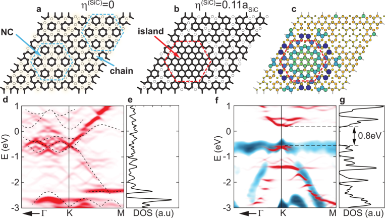
To study the electronic structure of the incommensurate system, we developed a tight binding model based on ab initio calculationsKim et al. (2008). Tight binding methods are often employed to study IC systems because of the large number of atoms involved. These IC calculations involve a “unit cell” arising from either a truncated lattice or by using a nearly commensurate lattice.Bak (1982); Voit et al. (2000); Sokoloff (1985); Ahmadieh and Rafizadeh (1973); Trambly de Laissardière et al. (2010). Although the Brillouin zone collapses in IC systems, delocalized dispersive states are still predicted for certain interaction configurationsSokoloff (1985, 1981). Indeed APRES measurements of IC systems still show “bands” .Voit et al. (2000)
The predicted metallic band structure can be recreated in a simplified tight binding (TB) calculation of the buffer graphene -bonds. In this model, a Si interface atom bonds to the nearest C atom in the buffer graphene if the in-plane C-Si distance is within a maximum radius, ( is determined from the ab initio calculations). The buffer -orbitals of the bonded carbon atoms are assigned an onsite potential consistent with the ab initio calculations and tight binding parameter estimates.Sup The excellent agreement between the ab initio and TB band structure is shown in Fig. 3(d). While both calculations are in agreement, they clearly do not predict the ARPES experimental semiconducting bands plotted in Fig. 3(f).
Within this TB ansatz (with a similar and on-site potential), we have explored the effect of a incommensurately modulated SiC lattice on the buffer’s band structure. In order to compare our calculations with measured ARPES bands, we begin with a commensurate unit cell. Significant changes occur in the C-Si bonding configuration when the bulk terminated surface is modulated according to Eq. 1.Sup Figure 3(b) shows the bonding structure using the experimentally measured . The modulation decreases the number of Si bonds to the buffer graphene layer by nearly 40% compared to the commensurate case in Fig. 3(a). Half of the NC regions in the commensurate structure converts into large regions of unperturbed graphene “islands” corresponding to half the low density regions in Fig. 2(b). The graphene between the islands, aligned with the high density boundaries in Fig. 2(b), have a much higher number of bonds to the interface Si as might be expected. The interface density modulation acts as a domain wall in the buffer graphene layer that breaks the bonding symmetry and opens a band gap. The formation of islands and the opening of a band gap occur for both larger “incommensurate” unit cells and over a large range of ’s () that includes the experimentally determined value of . The gap increases as a function of becoming nearly constant for .Sup
The calculated semiconducting bands [see Fig. 3(f)] look remarkably similar to the measured ARPES bands for (the experimental value). The predicted gap is eV as shown in density of states (DOS) in Fig. 3(g). The charge density from the three highest occupied bands in Fig. 3(f) show weak localization at the edges of the island [see Fig. 3(c)] and give rise to a charge density remarkably similar to STM measurements.Riedl et al. (2007)
When a monolayer of graphene (MG) forms above the buffer, there are changes in the buffer’s structure and electronic properties. We refer to the buffer with MG on top as to distinguish it from the bare buffer layer . While it is known that the buffer layer contracts when the monolayer forms [see Fig. 1(b)],Schumann et al. (2014) the reason for the change remains conjecture. SXRD shows that the buffer’s strain is due to a change in the modulation wavelength. Once the MG forms, the satellite rod positions and the lattice constant contract to a film nearly commensurate with the bulk SiC (i.e, ) [see Fig. 1(a)]. The MG lattice constant contracts relative to the making the MG incommensurate with both the and the SiC. The lattice constants for buffer and MG systems are summarized in Table 1.
Note that the MG lattice constant is within the range of values reported for theoretically isolated graphene, 2.453(4)Å.Weinert et al. (1982); Şahin et al. (2009); Wang (2010) This is consistent with models of weakly coupled layered materials (including graphite) where stronger interlayer interaction cause larger in-plane expansion.Barrera et al. (2005) The MG is contracted relative to graphite both because it interacts with a single layer and because the incommensuration between the two layers reduces the number of inter-layer bonds compared to Bernal stacking. This effect is analogous to the in-plane contraction observed in non-Bernal stacked graphene layers on C-face SiC [see Table 1].Hass et al. (2008)
The measured lattice constants show that graphene’s intrinsic strain has been historically misinterpreted using Raman 2D peak positions. It has been clearly demonstrated that the Raman 2D peak of tensile strained graphene red shifts to lower wave numbers.Zabel et al. (2012) Since isolated graphene must be compressively strained relative to graphite [see Table 1], the 2D peak of true free standing graphene must be blue shifted relative to graphite as is the case for the MG 2D peak.Ni et al. (2008); Rohrl et al. (2008); Speck et al. (2011); Fromm et al. (2013) The problem is that exfoliated graphene has its 2D peak shifted in the wrong direction (it is red shifted compared to graphite),Ni et al. (2008); Rohrl et al. (2008); Speck et al. (2011); Fromm et al. (2013) which contradicts its historical reference as “free standing” graphene. Clearly the position of the 2D Raman peak in “free standing” graphene is due to some other cause that has yet to be explained.
There are two other significant changes when the MG forms. First, the system becomes more disordered (30% decrease in long range order) evidenced by the broader satellite rods in Fig. 1(b). The also develops a large RMS strain, . RMS strain presents itself as a -dependent broadening (). As Fig. 1(c) shows, the has the largest slope (largest ) in a plot of vs [ data is summarized in Table 1]. The MG has a smaller RMS strain, presumably due to the weak coupling to the layer that allows strain relaxation.
Finally we address the buffer layer’s stability. It is assumed that the strong buffer-SiC interaction meant that the buffer’s band structure did not change significantly once the MG formed. Now that we have shown that there is a structural change in the buffer layer when the MG forms, it is prudent to revisit how or if the electronic structure is different from the layer. Figure 4(a) shows the ARPES spectra from the layer. The -bands are broad () consistent with the IC wavevector . In order to compare the bands with the , we have plotted a derivative spectra of the buffer and MG bands in Fig. 4(b) and (c). This compensates for both the broadening and the photoelectron attenuations through the MG.
Figure 4(c) shows that the semiconducting -bands are still present with the MG above. Although the bands intensity is weak, it is consistent with a complete buffer layer after correcting for attenuation. There is, however a change in the bands compared to the bands. The -bands are pushed to lower binding energy by eV compared to the bands and the band near appears to have less dispersion than the case. While there is a small energy gap between the layer bands and , the experimental error could also support the layer being metallic. We note that (the uncertainty is due to the increased disorder in the ). The low value of is consistent with a buffer layer structure closer to the commensurate structure that would give rise to either a very small gap or metallic bands.
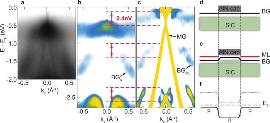
The band changes in the layer suggests a pnp junction device architecture by spatially controlling where MG is formed [see Fig. 4(d), (e), and (f)]. By first growing a continuous buffer layer, a capping layer (AlN or SiN) mask is locally deposited to inhibit further graphene growth.Rubio-Roy et al. (2010); Puybaret et al. (2015) The sample is then heated to grow MG outside of the masked area. This leaves a pnp junction as shown in Fig. 4 where the capping layer remains as a gate insulator.
Our x-ray measurements shows that the conventional assumption of a graphene film on SiC(0001) being commensurate with reconstruction is wrong. We find instead that first graphene “buffer” layer and a SiC interface layer have a mutual incommensurate density modulation. The modulation wavevector, gives rise to diffraction rods near (but not at) the positions explaining the misinterpretation of low resolution LEED data. The discovery answers a number of persistent and important questions about electronic and transport properties of both the buffer and the monolayer that grows above it. Using a simple model based on the experimental parameters from the incommensurate modulation, we show that the tight binding derived band structure is remarkably similar to the experimentally measured semiconducting bands. Our finding explain why ab initio calculations, based on a commensurate buffer-SiC system,Kim et al. (2008) predicts metallic -bands instead of the experimentally determined semiconductor bands.Emtsev et al. (2007); Nevius et al. (2015)
We also find that when a monolayer graphene layer grows on top of the buffer, it is incommensurate with the buffer. This incommensuration gives insight into why the monolayer graphene has a mobility an order of magnitude smaller compared to C-face graphene.Berger et al. (2006); Speck et al. (2010); Jobst et al. (2010) We suggest that because the monolayer is not periodic with the buffer below, a network of quasi-random monolayer-buffer interlayer coupling sites develop. These sites will increase random scattering in the film and thus lower the monolayer mobility. We also show that the buffer structure and corresponding band structure change when a monolayer grows above it. The band changes implies that a pnp junction can be created by locally growing a monolayer on an otherwise continuous buffer layer film. This effect suggests a new method for band gap engineering in graphene systems and potentially new architectures for graphene switching devices.
Author Contributions
E.H.C. supervised the project, designed and carried out the experiment, analyzed data and wrote the manuscript. M.C prepared samples, performed SXRD and ARPES experiments, analyzed data, performed TB calculations, and helped write the manuscript. F.W. performed SXRD experiments and analyzed data. M.S.N. prepared samples and edited the manuscript. K.J. helped analyze SXRD data. A. Ce., M.N.N., A.T-I, and A.T. performed ARPES experiments. Y.G., A.V. and A.Co helped perform SXRD experiments and critical reads of the manuscript. P.F.M. performed SXRD experiments, developed critical analysis of the SXRD results and critical reviews of the manuscript.
Experimental
The substrates used in these studies were n-doped CMP polished on-axis 4H-SiC(0001). The graphene was grown in a confinement controlled silicon sublimation furnace.de Heer et al. (2011) In the CCS method, graphene growth is a function of temperature, time, and crucible geometry that sets the silicon vapor pressure. With the current crucible design, a single semiconducting buffer graphene layer grows at a temperature of 1400for 30 min while a MLG film will grow above a buffer layer at 1560in 20 min. An important note is that once the MLG grows, a new buffer layer forms below the MLG layer. As we demonstrate, the buffer graphene with and without a MLG layer above it will be structurally different. The and MLG samples were characterized by Raman spectroscopy and LEED and give results similar to Fromm et al.Fromm et al. (2013) and Emtsev et al.Emtsev et al. (2008).
SXRD measurements were conducted at room temperature under UHV at the SIXS beamline at SOLEIL Synchrotron using a photon energy of keV. The angle of incidence was fixed at (near the critical angle) to optimize the scattered intensity. The momentum transfers, , are written in terms of the bulk hexagonal SiC lattice parameters: where and . represents a point in reciprocal space using SiC reciprocal lattice units (r.l.u.). Polarization and geometric correctionsVlieg (1997) were performed to compare integrated intensities. Prior to X-ray exposure, the samples were heated to 500in UHV to remove surface contaminants.
ARPES measurements were made at the Cassiopée beamline at the SOLEIL synchrotron. Measurements on both samples were performed at 90 K. The Fermi energy, , was determined from the k-integrated intensity cutoff of the molybdenum sample holder to within 20 meV for each sample. eV.
acknowledgement
This research was supported by the National Science Foundation under Grant No. DMR-1401193. P.F. Miceli also acknowledges support from the NSF under grant No DGE-1069091. Additional support came from the Partner University Fund from the French Embassy. The authors thank W. de Heer for use of the Keck Lab facilities, and A. Zangwill and M. Mourigal for many helpful discussions. We also wish to thank M. Kindermann and S. Spitz for help in the TB calculations. Finally, we with to thank the staff and technical support given for this project by the Synchrotron Soleil.
Supplemental Information
-
•
Supplemental Material: Diffraction intensity derivation, tight binding model and the incommensurate buffer graphene lattice constant
References
- Emtsev et al. (2007) K. V. Emtsev, T. Seyller, F. Speck, L. Ley, P. Stojanov, J. D. Riley, and R. C. G. Leckey, Mat. Sci. Forum 556-557, 525 (2007).
- Emtsev et al. (2008) K. V. Emtsev, F. Speck, T. Seyller, L. Ley, and J. D. Riley, Phys. Rev. B 77, 155303 (2008).
- Bommel et al. (1975) A. J. V. Bommel, J. E. Crombeen, and A. V. Tooren, Surface Science 48, 463 (1975).
- Forbeaux et al. (1998) I. Forbeaux, J.-M. Themlin, and J.-M. Debever, Phys. Rev. B 58, 16396 (1998).
- Varchon et al. (2007) F. Varchon, R. Feng, J. Hass, X. Li, B. N. Nguyen, C. Naud, P. Mallet, J.-Y. Veuillen, C. Berger, E. H. Conrad, and L. Magaud, Phys. Rev. Lett. 99, 126805 (2007).
- Mattausch and Pankratov (2007) A. Mattausch and O. Pankratov, Phys. Rev. Lett. 99, 76802 (2007).
- Kim et al. (2008) S. Kim, J. Ihm, H. J. Choi, and Y.-W. Son, Phys. Rev. Lett. 100, 176802 (2008).
- Nevius et al. (2015) M. S. Nevius, M. Conrad, F. Wang, A. Celis, M. N. Nair, A. Taleb-Ibrahimi, A. Tejeda, and E. H. Conrad, Phys. Rev. Lett. 115, 136802 (2015).
- Charrier et al. (2002) A. Charrier, A. Coati, T. Argunova, F. Thibaudau, Y. Garreau, R. Pinchaux, I. Forbeaux, J.-M. Debever, M. Sauvage-Simkin, and J.-M. Themlin, J. of Appl. Phys. 92, 5 (2002).
- Hass et al. (2006) J. Hass, R. Feng, T. Li, X. Li, Z. Zong, W. A. de Heer, P. N. First, E. H. Conrad, C. A. Jeffrey, and C. Berger, Appl. Phys. Lett. 89, 3 (2006).
- Riedl et al. (2007) C. Riedl, U. Starke, J. Bernhardt, M. Franke, and K. Heinz, Phys. Rev. B 76, 245406 (2007).
- van Landuyt et al. (1974) J. van Landuyt, G. van Tendeloo, and S. Amelinckx, Phys. Stat. Solidi (a) 26, K9 (1974).
- Vlieg (1997) E. Vlieg, Journal of Applied Crystallography 30, 532 (1997).
- Overhauser (1971) A. W. Overhauser, Phys. Rev. B 3, 3173 (1971).
- Cummins (1990) H. Z. Cummins, Physics Reports 185, 211 (1990).
- Perez-Mato et al. (1986) J. M. Perez-Mato, G. Madariaga, and M. J. Tello, Journal of Physics C: Solid State Physics 19, 2613 (1986).
- Schumann et al. (2014) T. Schumann, M. Dubslaff, M. H. Oliveira, M. Hanke, J. M. J. Lopes, and H. Riechert, Phys. Rev. B 90, 41403 (2014).
- (18) “See supplementary information,” .
- Goler et al. (2013) S. Goler, C. Coletti, V. Piazza, P. Pingue, F. Colangelo, V. Pellegrini, K. V. Emtsev, S. Forti, U. Starke, F. Beltram, and S. Heun, Carbon 51, 249 (2013).
- Emery et al. (2013) J. D. Emery, B. Detlefs, H. J. Karmel, L. O. Nyakiti, D. K. Gaskill, M. C. Hersam, J. Zegenhagen, and M. J. Bedzyk, Phys. Rev. Lett. 111, 215501 (2013).
- Vanević et al. (2009) M. Vanević, V. M. Stojanović, and M. Kindermann, Phys. Rev. B 80, 45410 (2009).
- Deretzis et al. (2014) I. Deretzis, G. Calogero, G. G. N. Angilella, and A. L. Magna, EPL (Europhysics Letters) 107, 27006 (2014).
- Bak (1982) P. Bak, Reports on Progress in Physics 45, 587 (1982).
- Voit et al. (2000) J. Voit, L. Perfetti, F. Zwick, H. Berger, G. Margaritondo, G. Grüner, H. Höchst, and M. Grioni, Science 290, 501 (2000).
- Sokoloff (1985) J. B. Sokoloff, Physics Reports 126, 189 (1985).
- Ahmadieh and Rafizadeh (1973) A. A. Ahmadieh and H. A. Rafizadeh, Phys. Rev. B 7, 4527 (1973).
- Trambly de Laissardière et al. (2010) G. Trambly de Laissardière, D. Mayou, and L. Magaud, Nano Letters 10, 804 (2010).
- Sokoloff (1981) J. B. Sokoloff, Phys. Rev. B 23, 6422 (1981).
- Hass et al. (2008) J. Hass, F. Varchon, J. E. Millán-Otoya, M. Sprinkle, N. Sharma, W. A. de Heer, C. Berger, P. N. First, L. Magaud, and E. H. Conrad, Phys. Rev. Lett. 100, 125504 (2008).
- Weinert et al. (1982) M. Weinert, E. Wimmer, and A. J. Freeman, Phys. Rev. B 26, 4571 (1982).
- Şahin et al. (2009) H. Şahin, S. Cahangirov, M. Topsakal, E. Bekaroglu, E. Akturk, R. T. Senger, and S. Ciraci, Phys. Rev. B 80, 155453 (2009).
- Wang (2010) S. Wang, J. Phys. Soc. of Japan 79, 64602 (2010).
- Nelson and Riley (1945) J. B. Nelson and D. P. Riley, Proceed. Phys. Soc. 57, 477 (1945).
- Baskin and Meyer (1955) Y. Baskin and L. Meyer, Phys. Rev. 100, 544 (1955).
- Bosak et al. (2007) A. Bosak, M. Krisch, M. Mohr, J. Maultzsch, and C. Thomsen, Phys. Rev. B 75, 153408 (2007).
- Barrera et al. (2005) G. D. Barrera, J. A. O. Bruno, T. H. K. Barron, and N. L. Allan, J. Phys: Cond. Mat. 17, R217 (2005).
- Zabel et al. (2012) J. Zabel, R. R. Nair, A. Ott, T. Georgiou, A. K. Geim, K. S. Novoselov, and C. Casiraghi, Nano Lett. 12, 617 (2012).
- Ni et al. (2008) Z. H. Ni, W. Chen, X. F. Fan, J. L. Kuo, T. Yu, A. T. S. Wee, and Z. X. Shen, Phys. Rev. B 77, 115416 (2008).
- Rohrl et al. (2008) J. Rohrl, M. Hundhausen, K. V. Emtsev, T. Seyller, R. Graupner, and L. Ley, Appl. Phys. Lett. 92, (2008).
- Speck et al. (2011) F. Speck, J. Jobst, F. Fromm, M. Ostler, D. Waldmann, M. Hundhausen, H. B. Weber, and T. Seyller, Appl. Phys. Lett. 99, (2011).
- Fromm et al. (2013) F. Fromm, P. Wehrfritz, M. Hundhausen, and T. Seyller, New J. of Phys. 15, 113006 (2013).
- Rubio-Roy et al. (2010) M. Rubio-Roy, F. Zaman, Y. Hu, C. Berger, M. W. Moseley, J. D. Meindl, and W. A. de Heer, Appl. Phys. Lett. 96 (2010).
- Puybaret et al. (2015) R. Puybaret, J. Hankinson, J. Palmer, C. Bouvier, A. Ougazzaden, P. L. Voss, C. Berger, and W. A. de Heer, Journal of Physics D: Applied Physics 48, 152001 (2015).
- Berger et al. (2006) C. Berger, Z. Song, X. Li, X. Wu, N. Brown, C. Naud, D. Mayou, T. Li, J. Hass, A. N. Marchenkov, E. H. Conrad, P. N. First, and W. A. de Heer, Science 312, 1191 (2006).
- Speck et al. (2010) F. Speck, M. Ostler, J. Röhrl, J. Jobst, D. Waldmann, M. Hundhausen, L. Ley, H. B. Weber, and T. Seyller, Mat. Sci. Forum 645-648, 629 (2010).
- Jobst et al. (2010) J. Jobst, D. Waldmann, F. Speck, R. Hirner, D. K. Maude, T. Seyller, and H. B. Weber, Phys. Rev. B 81, 195434 (2010).
- de Heer et al. (2011) W. A. de Heer, C. Berger, M. Ruan, M. Sprinkle, X. Li, Y. Hu, B. Zhang, J. Hankinson, and E. Conrad, Proc. Nat. Acad. of Sci. 108, 16900 (2011).