Ultra-low material pixel layers for the Mu3e experiment
Abstract
The upcoming Mu3e experiment will search for the charged lepton flavour violating decay of a muon at rest into three electrons. The maximal energy of the electrons is , hence a low material budget is a key performance requirement for the tracking detector. In this paper we summarize our approach to meet the requirement of about of a radiation length per pixel detector layer. This includes the choice of thinned active monolithic pixel sensors in HV-CMOS technology, ultra-thin flexible printed circuits, and helium gas cooling.
1 The Mu3e experiment
The Mu3e experiment [1] aims to search for the charged lepton flavor violating decay with a sensitivity to a branching ratio of ( C.L.) four orders of magnitude smaller than the current branching ratio limit of set by the SINDRUM experiment [2]. To achieve this goal within a reasonable time, more than muon decays per second have to be observed. An excellent momentum resolution of is required to distinguish between the signal decay and the dominant source of background, the decay [3]. Tracking detectors based on silicon pixel sensors are most suitable to meet the requirements on rate and resolution. As multiple scattering limits the momentum resolution, the whole detector has to be very thin. The material budget is limited to of a radiation length () per layer. Hybrid silicon pixel detectors offer high rate capabilities, however, the material budget is intrinsically too high as sensor and readout ASIC are two independent components. The high voltage monolithic active pixel sensor [4] (HV-MAPS) combines high speed and low material budget ( if thinned down to ) and is therefore chosen as technology for the experiment. A schematic of the planned barrel shaped tracking detector together with the scintilliating fibre and tile detectors used for precise time measurements is shown in figure 1. In this paper, the timing detectors will not be further discussed.

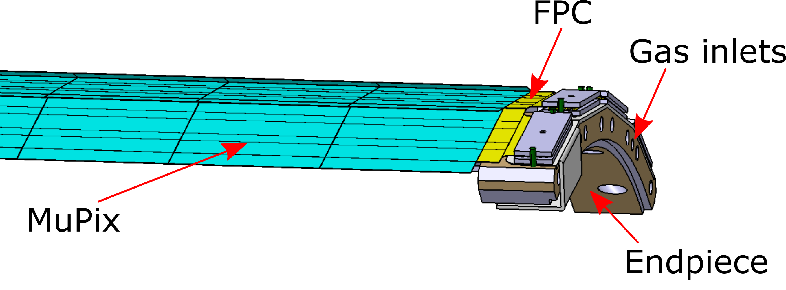
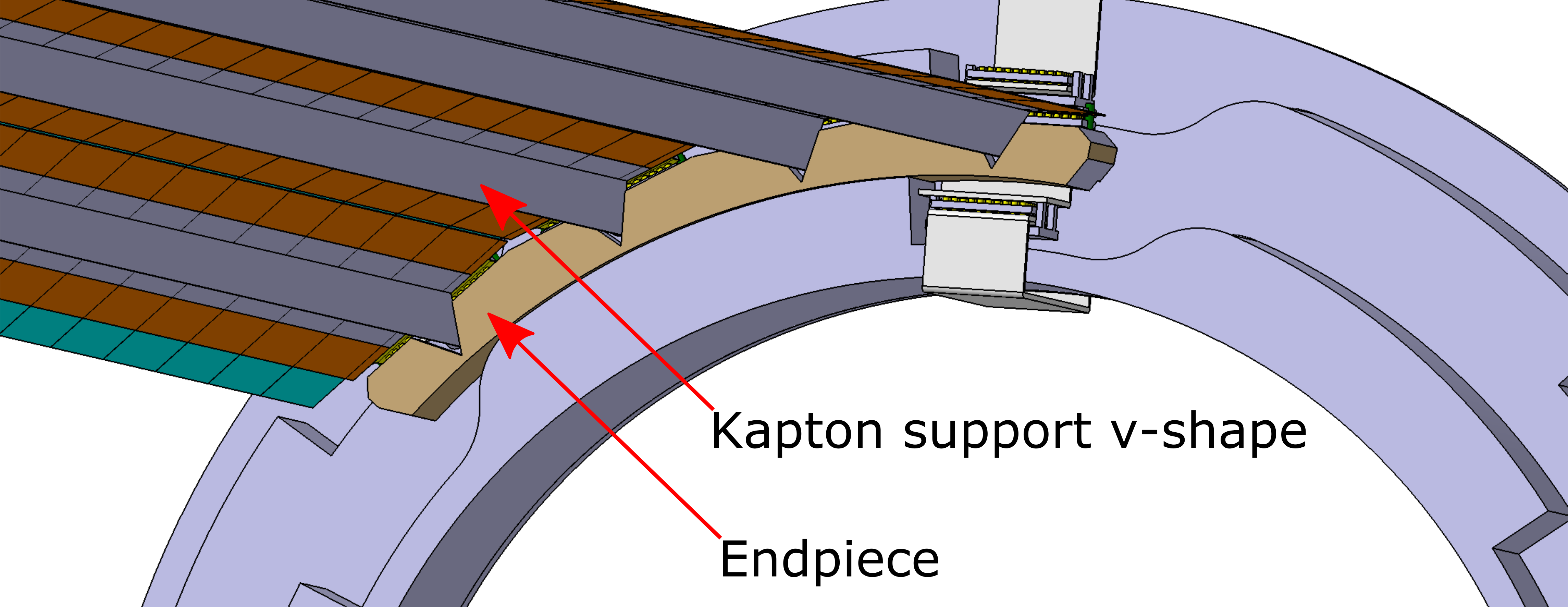
To meet the strict material budget requirement, the material of the interconnects, the mechanics and the cooling system inside the active detector volume has to be minimized. Therefore, thin aluminium flexible printed circuits (FPC) (), a mechanical support made from Kapton® foil (), and gaseous helium cooling are foreseen. The estimated peak material budget is about per tracking layer, taking up to of glue into account. A drawing of a Mu3e pixel module is shown in figure 2(a). A bottom view, where the v-shaped support structures can be seen, is depicted in figure 2(b). These v-shapes increase the mechanical stability and allow for additional helium gas flow close to the sensors.
The FPC technology currently under consideration and feasibility studies of an FPC prototype are presented in section 2. In section 3, the cooling concept for the Mu3e pixel detector is discussed.


2 Flexible printed circuits
The FPC provides all necessary connections for the pixel sensors. This includes the supplies (power, ground, and bias voltage) and signals (clock, reset, slow control and up to three fast data transmission lines). For the inner layers ( sensors, long), each sensor has three LVDS links at an output data rate of . For the outer layers ( sensors, long), only one data link per sensor is required due to the lower hit occupancy. The detector layers are electrically split in half with connectors at both ends. In order to minimize the material budget, aluminium is the preferred conductor material, saving a factor of four in material compared to copper for the same conductivity.
2.1 Technology
We currently explore two options for the FPCs. The first technology, called HiCoFlex [5] (by HighTec, Switzerland) uses very thin copper layers (few ) and allows for structure sizes down to a few . Our second option is an FPC manufactured by LED Technologies of Ukraine (LTU) [6]. Foils with of aluminium on of Kapton® are the raw material for the electrical layers. The FPC has two electrical layers separated by a dielectric spacing of made of Kapton® and glue required to match the differential impedance to . The minimum structure size is . The total FPC has an estimated thickness of , corresponding to a peak material budget of about . Bonding to sensors or PCBs as well as layer-to-layer vias are realized using the Single point Tape Automated Bonding (SpTAB) technique [7]. The advantage of this bonding method is that neither additional high Z materials nor fragile bonding wires are necessary.
2.2 Feasibility studies
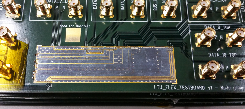
We performed feasibility studies with an FPC by LTU [8]. To this end we designed an FPC with test structures which was produced and bonded to a test PCB, see figure 3. Five identical prototypes were tested. The actual thickness of the FPCs was measured with a thickness gauge to be on average over the whole FPC, ranging from . The individual glue layers are estimated to have a thickness of , approaching the desired quite well. For a better control of the variations, the development of a special gluing jig is foreseen.
The resistance of dedicated low resistance power lines was measured using four-wire sensing. The results, between and depending on the trace length, are compatible with a conductor thickness of , significantly lower than . As the oxide layers of aluminium are typically only a few ten nanometers thin [9], they do not account for this reduction. Hence, we assume that aluminium is most likely lost during production in the etching process.

We tested the quality of high speed differential data transmission lines by using a bit error rate test. A PRBS7 pattern was generated and checked using an Altera Stratix V FPGA. At the experiment’s target data rate of we did not observe any errors in ten tested data traces over several hours, resulting in an upper limit on the bit error rate at the evel. Up to no bit errors were observed on a similar timescale, showing that the bandwidth margin is large.
The impedance of the differential transmission lines was analyzed using a time domain reflectometer. The traces were designed to match a differential impedance of using a trace width of and a gap of . We found that the impedance of most of the data traces is off by more than from the target. On the bottom layer, the distance between FPC and the first copper layer on the board was not taken properly into account in the design resulting in an impedance between . On the top layer, the impedance is measured to be higher than (around ) as the Kapton® foil, foreseen to be used for mechanical support in the experiment, was included in the design but not glued to the FPC for the measurements. Between the five different FPCs no significant variations are observed. The observed deviations are within expectations and are due to limitations of the experimental setup. For the final FPC the parameters will be adjusted to match the requirements.
3 Helium gas cooling for Mu3e
With a maximum power consumption of by the pixel sensors, the Mu3e silicon pixel detector will produce up to of heat, which has to be dissipated. The task of the Mu3e cooling system is to cool the sensors below and keep the material budget as low as possible. As gaseous helium has reasonable cooling capabilities and a large radiation length, important to avoid large multiple scattering, it is the coolant of choice. A schematic of the cooling concept indicating the different types of helium flow in the experiment is shown in figure 4.


Using a full CAD detector model, we performed computational fluid dynamics studies of the helium cooling [10]. Figure 5 shows the outcome of a simulation at the targeted sensor power consumption per area of . With the flow parameters given in figure 5, cooling of the detector below seems feasible. For higher power consumption, the flow velocities have to be increased.

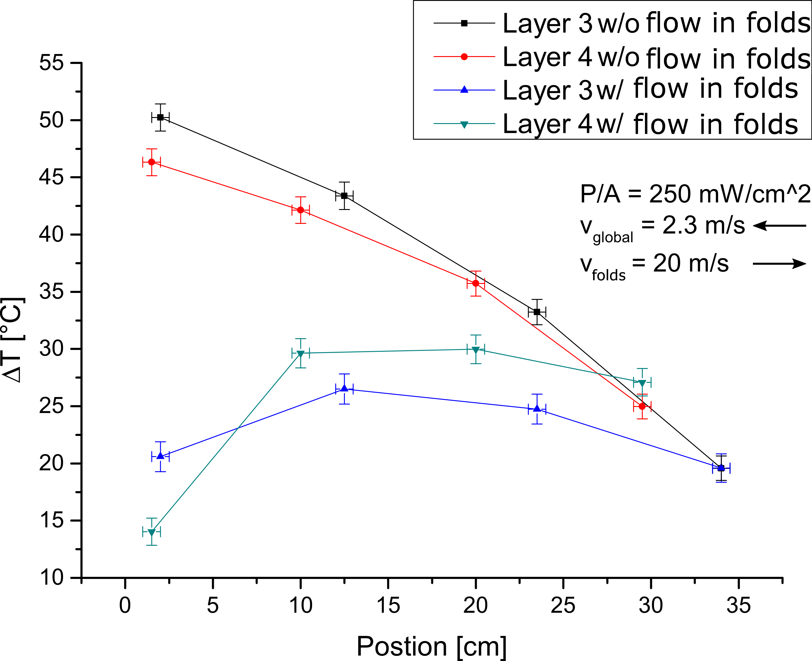
We performed cooling and mechanical studies in the laboratory with a large scale detector mockup using heatable, in-house manufactured, aluminized-Kapton® strips glued to thin glass plates. Figure 6 shows the measured temperature at different positions along a mockup module while it is heated with a power per area of [11]. The global helium flow enters to the right of the plot, thus the temperature increases towards position without helium flowing in the v-shaped folds. Using the v-shaped flow channels, the maximum temperature is decreased by more than and the temperature gradient along the module is significantly reduced. As the flow velocities, especially for the flow in the folds, are quite high, we tested the mechanical stability of the mockup with a Michelson interferometer. We found that it is mechanically very sturdy. Vibrations induced by cooling velocities up to were found to be below which is manageable for the final experiment [12].
4 Summary
For the Mu3e experiment, it is crucial that the material budget of the tracking detector does not exceed of a radiation length per layer. In our current design we estimate a peak material budget of about per layer, exceeding this limit slightly. But in order to achieve proper impedance matching on the FPC, there is not much material left that can be easily reduced. We achieved a first technological proof of concept for the FPC using an aluminium FPC prototype by LTU. We transferred data at our target data rate of successfully without any bit errors achieving a limit on the bit error rate on the level. The measured conductor thickness of allows to improve future FPC designs for the pixel modules. Simulation studies and laboratory tests show that a maximum temperature of the Mu3e detector below can be achieved using helium gas cooling.
Acknowledgments
The authors would like to express their gratitude to the team of LTU for the good cooperation. S. Dittmeier acknowledges support by the International Max Planck Research School for Precision Tests of Fundamental Symmetries. A. Herkert acknowledges support by the HighRR research training group [GRK 2058]. N. Berger acknowledges funding by the PRISMA cluster of excellence, Mainz, Germany, and wishes to thank Deutsche Forschungsgemeinschaft for support through the Emmy Noether program.
References
- [1] Blondel, A. et al., Research Proposal for an Experiment to Search for the Decay , arxiv:1301.6113.
-
[2]
Bellgardt, U. et al. and the SINDRUM Collaboration, Search for the Decay ,
Nucl.Phys. B299 (1988) 1. - [3] Djilkibaev, R.M. and Konoplich, R.V., Rare Muon Decay , Phys.Rev. D79 (2009) 073004.
- [4] Perić, I., A novel monolithic pixelated particle detector implemented in high-voltage CMOS technology, Nucl.Instrum.Meth. A582 (2007) 876.
- [5] HighTec MC AG, HiCoFlex - an ultra-thin, highly flexible Multilayer in 3rd International Workshop on Technology & Production - Processes for Flexible Electronic Systems, (2004).
- [6] LED Technologies of Ukraine, Kharkiv, Ukraine, Scientific Research, http://ltu.ua/en/scientific_research/detector_system/ (2016).
- [7] Abelev, B. et al and The ALICE Collaboration, Technical Design Report for the Upgrade of the ALICE Inner Tracking System, J. Phys. G: Nucl. Part. Phys. 41 (2014) 087002.
- [8] Noehte, L.O.S., Flexprint design and characterisation for the Mu3e experiment, B.Sc. thesis in preparation, University of Heidelberg (2016).
- [9] Jeurgens, L.P.H. et al., Structure and morphology of aluminium-oxide films formed by thermal oxidation of aluminium, Thin Solid Films 418 (2002) 89-101.
- [10] Ng, Y.W., Finite Element Analysis of the Cooling System for the Mu3e Experiment, M.Sc. thesis, University of Applied Science Jena and University of Heidelberg (2015).
- [11] Herkert, A., Gaseous Helium Cooling of a Thin Silicon Pixel Detector for the Mu3e Experiment, M.Sc. thesis, University of Heidelberg (2015).
- [12] Henkelmann, L., Optical Measurement of Vibration and Deformation of the Mu3e Silicon Pixel Tracker, B.Sc. thesis, University of Heidelberg (2015).