Cryogenic Characterization of FBK
HD Near-UV Sensitive SiPMs
Abstract
We report on the characterization of near-ultraviolet high density silicon photomultiplier (SiPM) developed at Fondazione Bruno Kessler (FBK) at cryogenic temperature. A dedicated setup was built to measure the primary dark noise and correlated noise of the SiPMs between 40 and 300 K. Moreover, an analysis program and data acquisition system were developed to allow the precise characterization of these parameters, some of which can vary up to 7 orders of magnitude between room temperature and 40 K. We demonstrate that it is possible to operate the FBK near-ultraviolet high density SiPMs at temperatures lower than 100 K with a dark rate below 0.01 cps/mm2 and total correlated noise probability below 35% at an over-voltage of 6 V. These results are relevant for the development of future cryogenic particle detectors using SiPMs as photosensors.
Index Terms:
Afterpulsing, avalanche photodiode, crosstalk, cryogenics, dark noise, silicon photomultiplier (SiPM).I Introduction
The use of silicon photomultipliers (SiPMs) at cryogenic temperatures is a new line of development with increasing interest from a wide range of scientific fields. SiPM operation at cryogenic temperatures offers an interesting option for future particle detectors, where the detection efficiency of scintillation light is of primary importance.
Building on its strong line of SiPM development [1], FBK recently introduced a new generation of near-ultraviolet high density (NUV-HD) SiPMs. The performance of NUV-HD SiPMs detailed in [2], makes them a promising candidate for use in future, multi-ton dark-matter detectors. One such detector is DarkSide-20k, a tonne dual phase argon time projection chamber that will require about of near-UV sensitive photodetectors operating at with very low noise. In this paper, we present measurements of the cryogenic performance of NUV-HD SiPMs including the dark count rate (DCR) and the correlated noise.
We characterized two variants of the NUV-HD SiPMs, the NUV-HD standard-field (NUV-HD-SF) and the NUV-HD low-field (NUV-HD-LF), which differ by the field strength in the avalanche region [3]. All the NUV-HD SiPMs tested were with a cell pitch of .
To perform these measurements, we developed a cryogenic test setup equipped with a flexible data acquisition system and an ad-hoc analysis tool, capable of characterizing SiPMs and SiPM assemblies in the temperature range from .
Section II is devoted to the cryogenic experimental setup, Sections III and IV show the data acquisition system and the analysis tool. In Section V, we detail the results obtained for the NUV-HD SiPMs.
II Cryogenic Setup
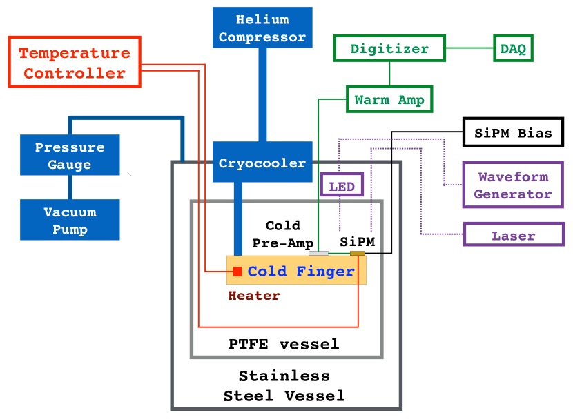
The cryogenic setup is contained in a stainless steel vacuum chamber made of a cylindrical tube closed by two DN 320 ISO-K flanges. Inside the vacuum chamber sits a thin PTFE (Polytetrafluoroethylene) cylinder shielded by a layer of superinsulator that serves as a thermal shield. The cryostat is equipped with a set of vacuum bulkhead feedthroughs. Several coaxial SMA connections are used for the SiPM signal. A set of hermetic, high density connectors are used for temperature readout, heater power, pre-amplifier power and SiPM bias. A hermetic optical fiber feedthrough is installed so that the device under test can be illuminated by an external laser source; a blue LED is installed in the cryostat and can also be used to illuminate the SiPM. To minimize light leaks, which could spoil the dark rate measurements, a small dark box was built to contain the SiPM, as described later in this section. Furthermore, opaque fabric is wrapped around the cryostat to further reduce the light entering the chamber. An overview sketch of the system is shown in Fig. 1.
During operations, the chamber reaches a vacuum level of about thanks to a Pfeiffer ACP15 multi-stage roots evacuation pump. A Cryomech PT90 pulse tube cryocooler, capable of delivering of cooling capacity at , is mounted on the top of the flange. The cold head of the cryocooler is equipped with a cold finger, which holds the SiPM assembly under test. This arrangement allows for fast thermal cycling: the cold finger can be thermalized from room temperature to in about minutes. The cold finger also hosts a platinum surface mount RTD soldered to a printed circuit board (PCB) and connected via low thermal conductance phosphor bronze wires to a Lakeshore 335 temperature controller, which regulates the temperature by driving a set of high power metal film resistors mounted on the cold finger. This system has proven to reach a temperature stability of about and an accuracy of about in the range of interest from . A Lakeshore 218 meter measures the temperature of other platinum RTD sensors installed in the cryostat.
To minimize unwanted thermal gradients, SiPMs are mounted on -thick aluminum PCBs that use insulated metallic substrate (IMS) technology with the silver-loaded conductive epoxy MasterBond EP21TDCS-LO. The mounted SiPM is firmly connected to the cold finger by a screw, with a thin layer of cryogenic grease ensuring a good thermal contact between the copper and the aluminum board. A cryogenic pre-amplifier specifically designed for this application is connected to the SiPM and is in thermal equilibrium with the cold finger.
III Readout Chain and Data Acquisition System
The readout chain is composed of:
-
•
a SiPM bias source;
-
•
a cryogenic pre-amplifier directly connected to the device under test and the bias supply;
-
•
a low noise warm amplifier that receives the signal from the pre-amplifier;
-
•
and a high speed digitizer.
A Keithley 2450 SourceMeter is used to provide the bias voltage to the SiPM. This unit can directly measure the current-voltage () curves of the SiPM useful to measure both the breakdown voltage and the value of the quenching resistor.
The cryogenic pre-amplifier is a high speed, low noise operational amplifier configured as a trans-impedance amplifier (TIA) with a feedback resistor of resulting in a gain of . This configuration allows a reasonable sensitivity despite the very large SiPM input capacitance of . The pre-amplifier has a resistor between the SiPM and the TIA to reduce the noise gain of the amplifier at high frequencies and to better match the signal from the SiPM with the amplifier, thus avoiding undershoots [4]. The design and the implementation of the cryogenic pre-amplifier will be discussed in a future publication.
The warm amplifier consists of a single stage non-inverting amplifier with input noise equivalent of , significantly smaller than the output noise from the cryogenic pre-amplifier. The device is configured for a gain of with a rise time of .
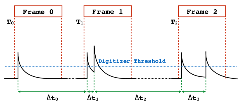
The amplified signal is fed into a CAEN V1751 digitizer configured for interleaved acquisition and operating in auto-trigger mode. Each time the digitizer signal crosses a fixed threshold the waveform is recorded for a fixed time duration (i.e. frame). Each saved frame is set to contain a sufficient number of points before the trigger time position to enable an estimation of the baseline level. A custom C++ program handles the configuration and the readout of the digitizer. Data are saved in a custom file format, with each frame in the file including the digitized waveform and a header that contains accurate timing information – see Fig. 2.
Two time stamps, a fine and a coarse counter, are saved for each frame. The first is obtained directly by the digitizer and represents the starting time of each frame counting from the beginning of the measurement. It has a resolution of and an overflow time of roughly . In order to recover the time information when the acquisition time exceeds the overflow, which can easily be the case with the low event rate expected at cryogenic temperature, an additional coarse counter is extracted by the operating system of the computer with a lower precision (on the order of ).
The trigger threshold value is set by the user depending on the device under test, the noise level and the signal gain. It is typically set to be half of the value of the amplitude of a single cell response. The length of the acquisition gate depends on the pulse rate from the SiPM. At cryogenic temperatures, the low rate enables the use of a short, gate, with each frame typically recording a single SiPM pulse. Near room temperature, the gate is set to , resulting in many pulses being recorded in the same frame. In this case, time differences between consecutive pulses are evaluated by analyzing the waveform only.
IV The Data Analysis Software
The data analysis software was developed at FBK following the procedure described in [5]. It reads the data stored in the data frames and performs a detailed analysis of the SiPMs response, with special emphasis on the time correlation of pulses. The analysis capabilities are strongly enhanced by the addition of the time tagging of frames previously described in Sec. III, which is mandated by the several order of magnitude variation in SiPM dark pulse rates as a function of temperature. The time tagging of frames allows the time difference between consecutive pulses to be calculated from the nanosecond scale, using pulses within the same frame, to thousands of seconds, using different frames, with the only practical limit set by the time available for measurement. This allows a seamless determination of the temperature-dependent SiPM pulse rate, a detailed study of their correlation, and the extraction of the secondary noise probabilities.
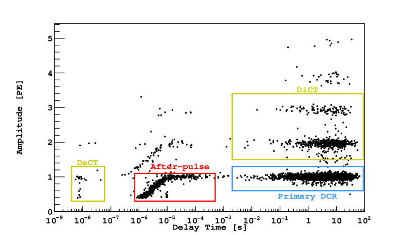
For data collected near room temperature, the frame time tag is not helpful, as each frame may already contain several hundreds of events and the dead time required by the digitizer to store the data becomes comparable with the inverse of the dark rate. Except for this difference in the utilization of data, the analysis is uniform for all dataset: each event is tagged with an ordered pair of values, i.e. the time distance from the previous pulse and the amplitude. A typical scatter plot with ordered pairs recorded for a run at and in absence of light stimulation is shown in Fig. 3. The plot allows the identification of the different kinds of pulses that compose the noise response of the SiPM.
-
DCR:
The main group of events is due to primary, Poisson-distributed, dark counts that make up the DCR. The amplitude is centered at around (Photo-Electron), and the distribution in time is exponential with a decay time corresponding to the inverse of the DCR.
-
DiCT:
Direct CrossTalk (DiCT) events occur a very short time after the preceding pulse, given by the travel time needed for the crosstalk photon to reach a neighboring cell and trigger an independent avalanche. The time required is on the picosecond time scale, nearly impossible to be resolved with the readout electronics. As a result, DiCT pulses are superimposed on the DCR pulses and have a similar time distribution but are characterized by greater amplitudes corresponding to the detection of or more .
-
DeCT:
The less populated groups with characteristic delay times of few to tens of nanoseconds are due to Delayed CrossTalk (DeCT). These events are caused by crosstalk photons absorbed in the non-depleted region of a neighboring cell. The carriers diffuse for a short time before reaching the high-field region and finally triggering an avalanche. The resulting pulse has the single cell amplitude but is delayed with respect to the previous by the characteristic diffusion time, typically on the order of few to tens of nanoseconds. Such delayed pulses can further trigger DiCT pulses, yielding events with the same time distribution but higher amplitudes.
-
AP:
Finally, the group of events with intermediate delay times and amplitude of or lower are identified as AfterPulsing (AP). Afterpulsing occurs when, during an avalanche, an electron is trapped by some impurity in the silicon lattice and is then released after a characteristic time, generating a second avalanche. Since the afterpulsing event and its primary avalanche occur in the same cell, the time distribution is determined by both the traps time constants and the recharge time constant of the microcell. When the time distance is lower than the full micro-cell recharge, the resulting pulse has a reduced amplitude. As with the other types of events, they can trigger DiCT pulses, explaining the higher amplitude groups with the same time distribution.
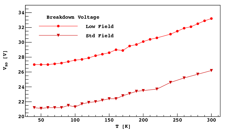
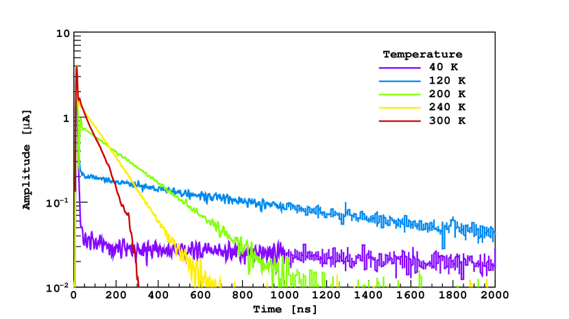
That analysis software saves the following parameters: primary DCR, correlated noise probabilities (DiCT, DeCT and AP), and single cell signal features (amplitude, recovery time, and charge delivered in a fixed time gate). Also stored is the waveform amplitude resulting from the application of the differential leading edge discriminator (DLED) algorithm, as defined in [6], which is useful for evaluating the breakdown voltage since the resulting peak amplitude is linear with the applied over-voltage. Measuring the DLED amplitude as a function of over-voltage typically allows for a more precise determination of (Fig. 4) than what can be derived from the curve. This method allows a precise determination of the over-voltage as a function of temperature. In order to compare the SiPM DCR as a function of temperature, it is important that each point is taken at the same over-voltage. Therefore, any plot of DCR vs. over-voltage is re-corrected in the analysis stage by performing a linear interpolation of the data to extract the correct DCR at the exact value of over-voltage as determined with this procedure. The same consideration applies for all the other SiPM features.
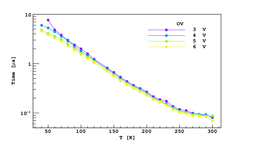
The SCRis defined as the signal generated at the output of the amplifier when a single microcell of the SiPM fires. All the single photon avalanche diodes (SPADs) contained in the SiPMs under test are passively quenched with a polysilicon resistor, whose quenching resistance is denoted with . The impedance of this material depends strongly on temperature, increasing with decreasing temperature, and affects various signal features. The typical SiPM pulse is made up of two components, a fast one, whose time constant is of the order of few nanoseconds, and a slow component, whose time constant can extend to several microseconds and corresponds to the SPAD recharge time. The electric model proposed in [7] is well suited to describe the SiPM behaviour. The slow time constant is expected to be proportional to the quenching resistance, as in , where is the parasitic capacitance of the polysilicon resistor. With decreasing temperature, the increase in translates to higher values of . This effect is clearly seen in Fig. 5.
V Experimental Results
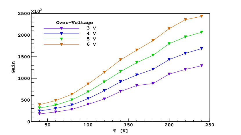
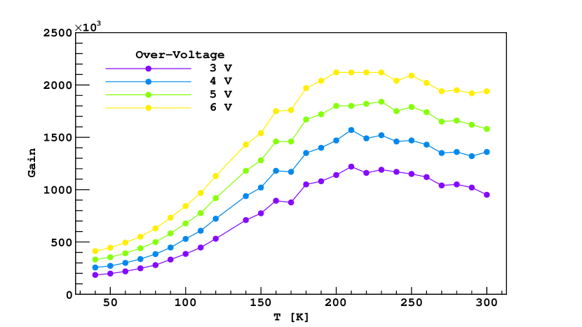
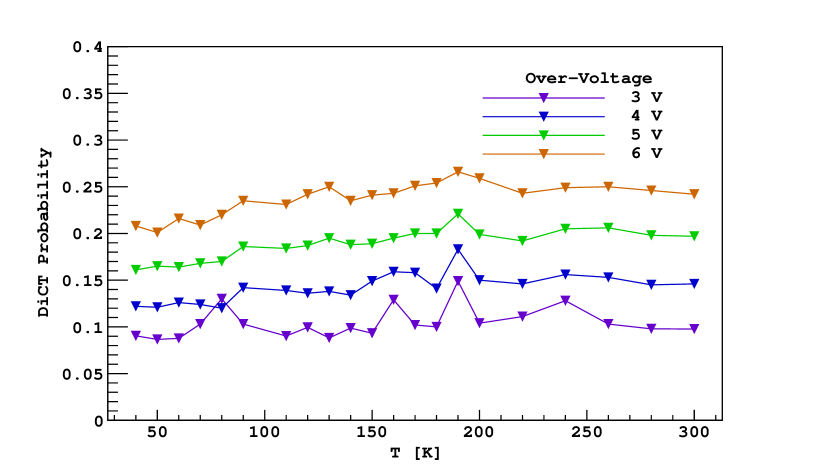
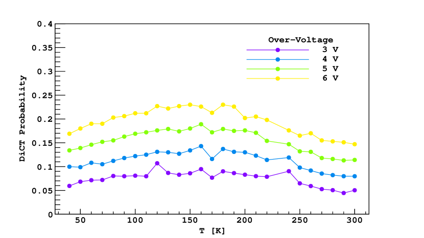
The analysis program described in Sec. IV fits the recharge (recovery) time for the individual SPAD waveform as a function of over-voltage and temperature. The result is shown in Fig. 5: NUV-HD-SF and NUV-HD-LF SiPMs exhibit the same exponential trend, with a slight difference in overall results.
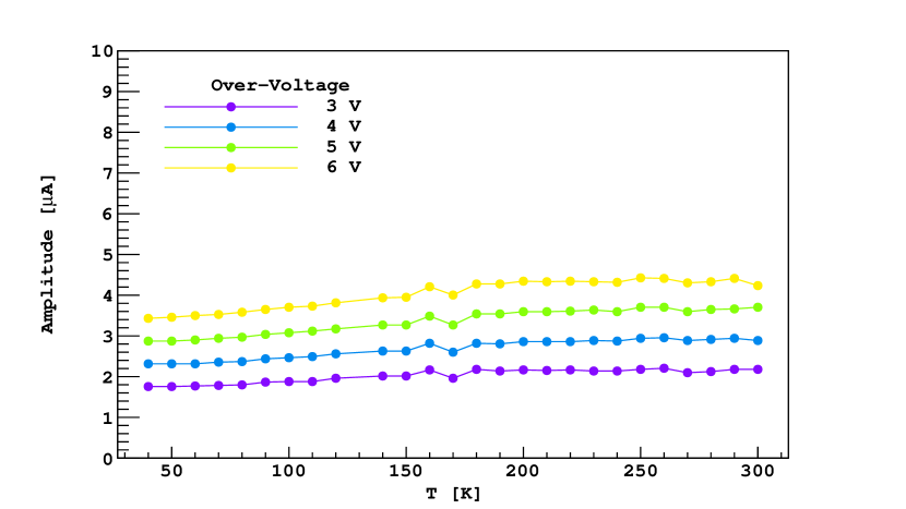
The peak amplitude of the SCR is mainly determined by the fast peak. Its amplitude increases linearly with over-voltage and only very slowly with temperature (see Fig. 6).
For each pulse, the overall charge released (or gain) is measured by comparing the result of the integration of the signal in two fixed and equal gates, one containing the pulse and one the baseline. By measuring the distance between the peaks of the resulting distributions and considering the amplification factors of the front-end electronics, it is possible to calculate the number of carriers generated in the SPAD. Again, the two variants of the NUV-HD technology show similar results, see Fig. 8. The variation with temperature is due to the fact that with decreasing temperature and longer pulses, an increasingly larger fraction of the total pulse sits out of the integration gate. Near room temperature, when the signal duration becomes shorter than the integration time, the gain is expected to saturate to a plateau. The residual dependence on temperature observed is due to the variation with temperature of the depletion width of each SPAD for a given over-voltage. This happens because the breakdown voltage changes with temperature as well. Therefore, we also observe a variation of the SPAD junction capacitance and thus of its gain.
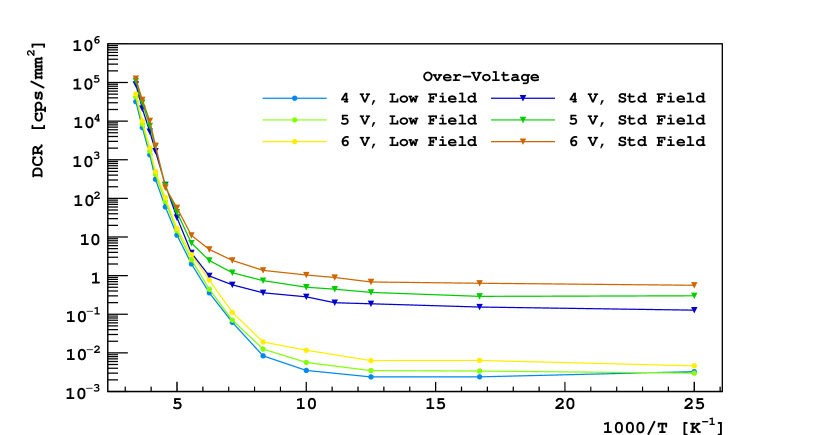
The NUV-HD-LF SiPMs are optimized to achieve a significant noise reduction at low temperature and exhibit a DCR that is one to two orders of magnitude lower than the NUV-HD-SF at the same over-voltage, see Fig. 7. An Arrhenius plot of the DCR over the entire temperature range of interest clearly seperates the two different mechanisms responsible for the dark rate generation. Thermal generation dominates at high temperatures [8, 9], while at low temperature the main contribution originates from tunneling [10]. Due to the lower electric field value, the magnitude of the latter component is highly suppressed in NUV-HD-LF SiPMs.
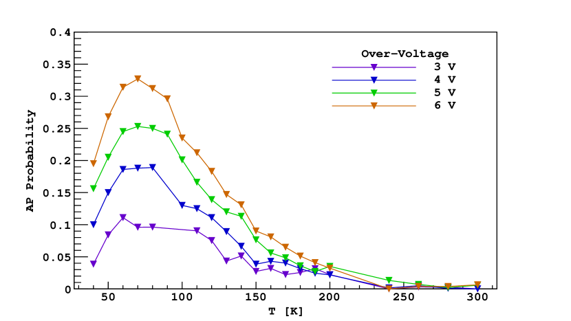
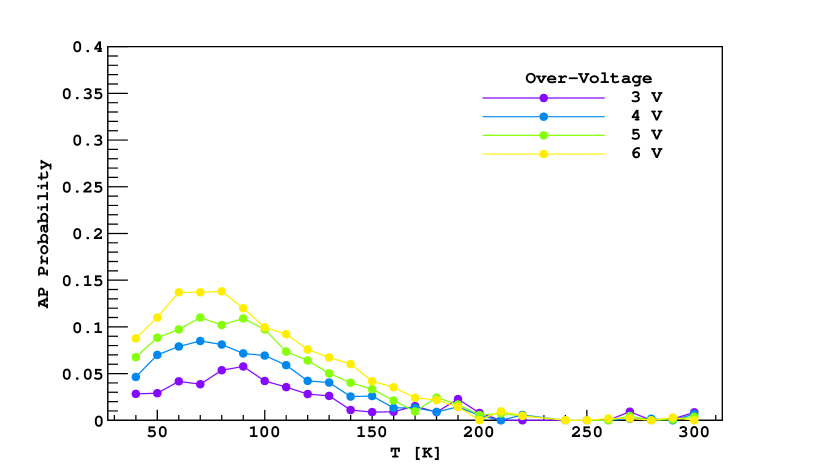
The NUV-HD-LF SiPMs present lower correlated noise than the NUV-HD-SF SiPMs at the same OV, see Fig. 9, 10. This is explained with the overall lower gain and avalanche triggering probability in the NUV-HD-LF devices. The DiCT exhibits only a weak dependence on the temperature, while it is linear in over-voltage, see Fig. 9. The difference between the two technologies AP probability cannot be ascribed only to the lower gain of the devices but probably also to a suppression of some field effects contributing to this noise component. The AP probability reaches a maximum in the temperature range from and then decreases to zero in the high temperature region. This peculiar dependence can be explained by the interplay of two different phenomena having opposite effects on the noise probability. At low temperatures, the trapping time constants increase, enhancing the probability of a carrier to be released when the cell is at least partially recharged, producing an AP event. On the other hand, the quenching resistance grows exponentially (see Fig. 5), thus suppressing the avalanche triggering probability during the recharge. The DeCT probability is very low in both technologies, having a maximum value of , and it is not shown.
VI Conclusions
We developed a cryogenic setup equipped with a robust data acquisition system that is suitable for a broad variety of tests on SiPMs as a function of temperature in the interval from . This system is complemented by a comprehensive analysis software based on a set of tools used at FBK and optimized to work in a wide range of count rates. The NUV-HD-LF SiPMs performance at cryogenic temperature is impressive, with a DCR as low as . Further design work for the optimization of the value of the quenching resistor as well as for the further reduction of the field in the avalanche region (and consequently of the DCR) is ongoing at FBK. Measurements of the PDE of the NUV-HD are ongoing as well as a full cryogenic characterization of the FBK RGB-HD family of SiPMs.
References
- [1] C. Piemonte, “A new Silicon Photomultiplier structure for blue light detection,” Nucl. Inst. Meth. A, vol. 568, no. 1, pp. 224–232, Nov. 2006.
- [2] C. Piemonte, F. Acerbi, A. Ferri, A. Gola, G. Paternoster, V. Regazzoni, G. Zappala, and N. Zorzi, “Performance of NUV-HD Silicon Photomultiplier Technology,” IEEE Trans. Elec. Dev., vol. 63, no. 3, pp. 1111–1116, 2016.
- [3] A. Ferri, F. Acerbi, A. Gola, G. Paternoster, C. Piemonte, and N. Zorzi, “Performance of FBK low-afterpulse NUV silicon photomultipliers for PET application,” JINST, vol. 11, no. 03, pp. P03 023–P03 023, Mar. 2016.
- [4] A. Gola, C. Piemonte, and A. Tarolli, “Analog Circuit for Timing Measurements With Large Area SiPMs Coupled to LYSO Crystals,” IEEE Trans. Nucl. Sci., vol. 60, no. 2, pp. 1296–1302, 2013.
- [5] C. Piemonte, A. Ferri, A. Gola, A. Picciotto, T. Pro, N. Serra, A. Tarolli, and N. Zorzi, “Development of an automatic procedure for the characterization of silicon photomultipliers,” IEEE Conf. Pub., pp. 428–432, 2012.
- [6] A. Gola, C. Piemonte, and A. Tarolli, “The DLED Algorithm for Timing Measurements on Large Area SiPMs Coupled to Scintillators,” IEEE Trans. Nucl. Sci., vol. 59, no. 2, pp. 358–365, Apr. 2012.
- [7] F. Corsi, A. Dragone, C. Marzocca, A. Del Guerra, P. Delizia, N. Dinu, C. Piemonte, M. Boscardin, and G. F. Dalla Betta, “Modelling a silicon photomultiplier (SiPM) as a signal source for optimum front-end design,” Nucl. Inst. Meth. A, vol. 572, no. 1, pp. 416–418, Mar. 2007.
- [8] R. N. Hall, “Electron-Hole Recombination in Germanium,” Phys. Rev., vol. 87, no. 2, pp. 387–387, Jul. 1952.
- [9] W. Shockley and W. T. Read, “Statistics of the Recombinations of Holes and Electrons,” Phys. Rev., vol. 87, no. 5, pp. 835–842, Sep. 1952.
- [10] M. Ghioni, A. Gulinatti, I. Rech, P. Maccagnani, and S. Cova, “Large-area low-jitter silicon single photon avalanche diodes,” Proc. SPIE, vol. 6900, pp. 69 001D–69 001D–13, Jan. 2008.