Capacitively coupled pickup in MCP-based photodetectors using a conductive metallic anode
Abstract
We have designed and tested a robust 20 20 cm2 thin metal film internal anode capacitively coupled to an external array of signal pads or micro-strips for use in fast microchannel plate photodetectors. The internal anode, in this case a 10nm-thick NiCr film deposited on a 96% pure Al2O3 3mm-thick ceramic plate and connected to HV ground, provides the return path for the electron cascade charge. The multi-channel pickup array consists of a printed-circuit card or glass plate with metal signal pickups on one side and the signal ground plane on the other. The pickup can be put in close proximity to the bottom outer surface of the sealed photodetector, with no electrical connections through the photodetector hermetic vacuum package other than a single ground connection to the internal anode. Two pickup patterns were tested using a small commercial MCP-PMT as the signal source: 1) parallel 50 25-cm-long micro-strips with an analog bandwidth of 1.5 GHz, and 2) a 20 20 cm2 array of 2-dimensional square ‘pads’ with sides of 1.27 cm or 2.54 cm. The rise-time of the fast input pulse is maintained for both pickup patterns. For the pad pattern, we observe 80% of the directly coupled amplitude. For the strip pattern we measure 34% of the directly coupled amplitude on the central strip of a broadened signal. The physical decoupling of the photodetector from the pickup pattern allows easy customization for different applications while maintaining high analog bandwidth.
keywords:
Fast timing, Microchannel-plate photomultipliers (MCP-PMT), Large Area Picosecond Photodetectors (LAPPD), Anode, Capacitive coupling1 Introduction
Microchannel-plate photomultipliers (MCP-PMT) are specialized vacuum photodetectors typically consisting of a photocathode, an amplification section consisting of several planes of glass micropores, and a segmented anode from which the amplified pulses are detected [1]. A hermetic package provides internal vacuum, mechanical support, and electrical connections. The photocathode is typically on the inside face of the top window; the anode electrodes are integrated into the bottom plate of the package.
Unlike conventional photomultipliers that focus the photoelectrons from the photocathode onto a discrete chain of smaller dynodes, the microchannel-plate photomultiplier is planar with a uniform transverse structure. The photocathode is proximity-focused onto the amplification section, which in turn is proximity-focused onto the anode plane. This geometry in principle enables excellent spatial resolution with a minimum scale size of a pore diameter, and excellent time resolution, set by jitter in the primary photoelectron time of ‘first strike’ and jitter in the first few interactions in the amplification electron cascade [2]. Large (20 20 cm2 ) MCPs made from a glass substrate with resistive and secondary-emitting layers formed with Atomic Layer Deposition have demonstrated gains greater than 107, time resolutions measured in 10’s of picoseconds, and spatial resolutions on the order of 700 microns [2, 3].
The spatial and temporal resolutions are determined by the conversion of the electron cascade pulse at the anode plane into a measurable signal, and also by the transport of that signal through the package wall to the digitizing electronics. Spatial resolutions of a few microns can be obtained with anodes consisting of delay lines [3, 4], time resolutions of a few 10’s of picoseconds are measured using radio-frequency (RF) micro-strip delay lines [2, 5, 6]. Two-dimensional arrays of pads allow a compromise, maintaining good resolution in both space and time [7, 8], but with many external connections if the array is to have small pixels.
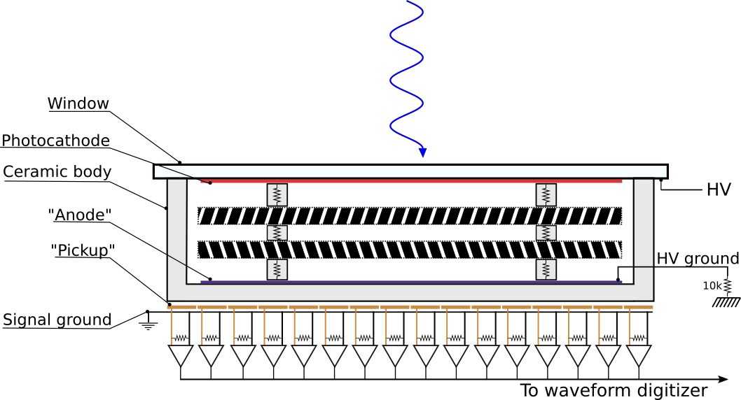
In a capacitively coupled configuration, shown in Fig. 1, the charge shower from the MCP amplification section induces a current in a metallic anode deposited on the bottom plate of the detector package. The signal pickup consists of an array of conductors and a signal ground. The pickup electrodes capacitively couple to currents on the internal anode, producing a signal relative to the signal ground.
Traditionally, the anode readout pattern is sealed in the vacuum packaging of the photodetector, and cannot be modified after fabrication. In contrast, the capacitively coupled readout pattern is separate from the detector, mounted outside of the MCP-PMT vacuum packaging. The signal pickup can then be optimized for different applications with different requirements on time resolution, spatial resolution, and channel occupancy. The photodetector module and capacitive pickup board can be manufactured independently.
Capacitively coupled MCP-PMT anodes have been successfully demonstrated using resistive thick films or semi-conductors [9, 10, 11, 12, 13], and MCP-PMTs using them are commercially available [11, 16]. Here we demonstrate that a thin metal layer can also transmit the high-frequency components of the fast pulses from an MCP-PMT to an external array of electrodes.
The development and testing of the metal-film capacitively coupled anode has been done in the context of the commercial development of 20 20 cm2 MCP-PMTs [17] following the R&D of the LAPPD Collaboration [18]. Metal film deposition is widely available commercially, and making a uniform metal anode on the interior of an LAPPDTM module has proved to be much easier than silk-screening and firing a resistive film. In addition, since metal film deposition is often already part of the process of photodetector packaging, the deposition of an anode metal film can be easily integrated into the manufacturing.
2 Anode and Signal Pickup Implementation
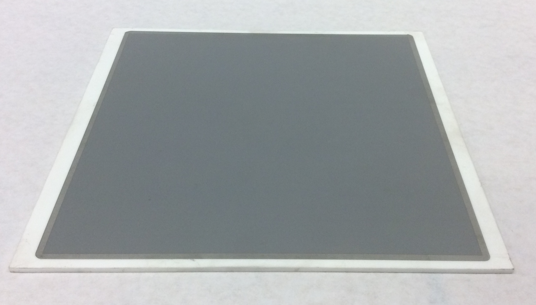
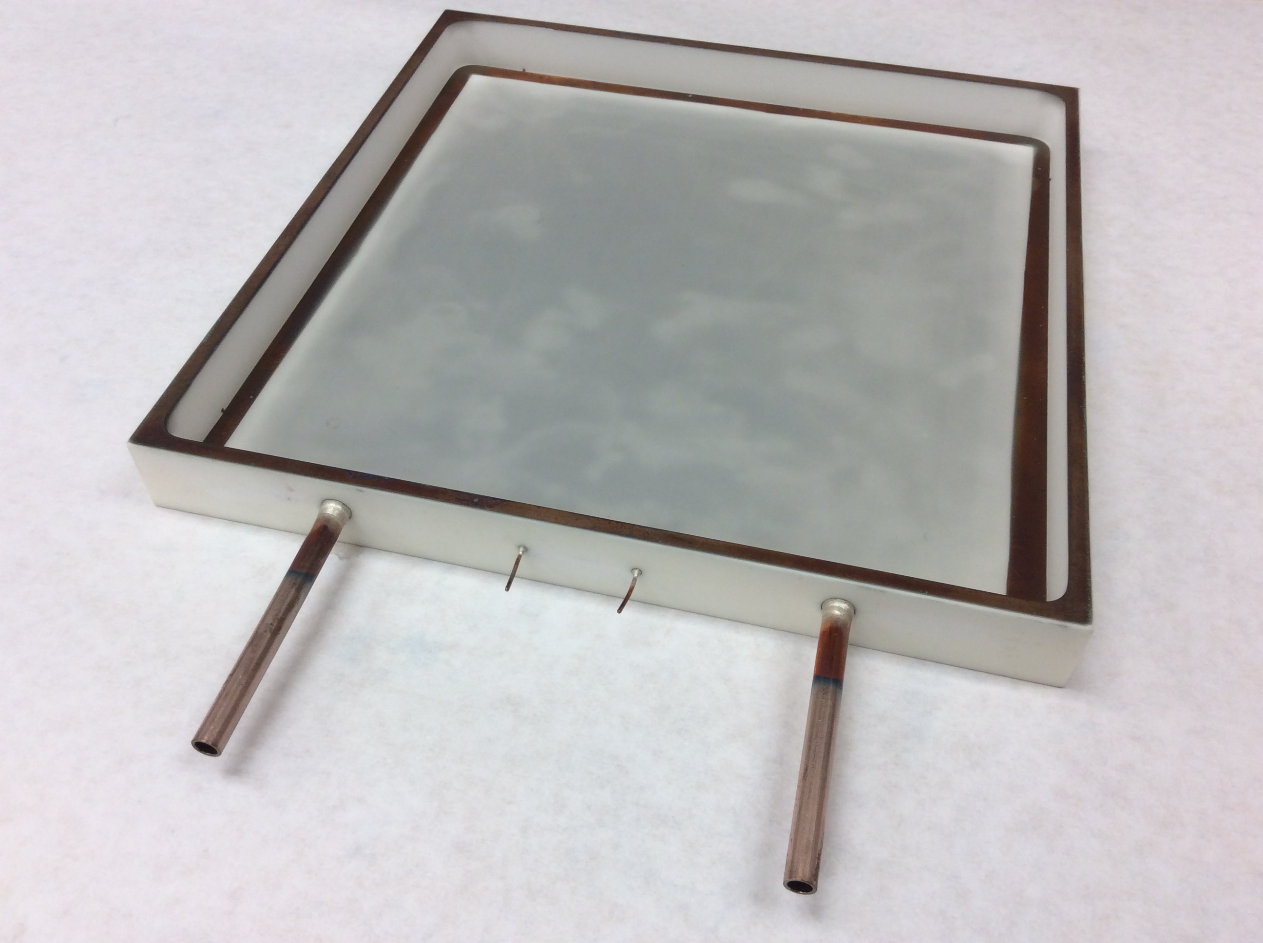
Testing has been done on a ceramic substrate that replicates the bottom plate of a ceramic MCP-PMT package, shown in Fig. 2. The 20 20 cm2 NiCr metal anode is the same for the test substrate and for the MCP-PMT package [19], and is described in Section 2.1. The two pickup geometries, one of two-dimensional pads and the other of micro-strips, are described in Section 2.2.
2.1 Ceramic/NiCr Anode Plane and Photodetector Package
The test anode was constructed by evaporating a 10-nm-Nichrome (NiCr) [20] film onto a 3-mm-thick alumina-ceramic substrate [21]. In an operational MCP-PMT the ceramic substrate acts as the bottom layer of the hermetic package, with the anode on the inner surface. The NiCr film of the anode has a sheet resistance of per square.
2.2 Signal Pickup Arrays
The geometric layout of readout conductors determines the temporal and spatial resolutions of the photodetector. Typical anode patterns include transmission-line micro-strips [6], two-layer crossed delay lines [4, 9], and pad arrays [8].
Tests were performed using two separate signal pickups, one consisting of 50 micro-strips, and the other an array of 2-dimensional pads. The strip pickup, shown in the left-hand panel of Figure 3, consists of silver strips fired onto a glass substrate [6]. This pickup has an analog bandwidth of 1.5 GHz and good signal characteristics up to a length of 90-cm [2, 6].
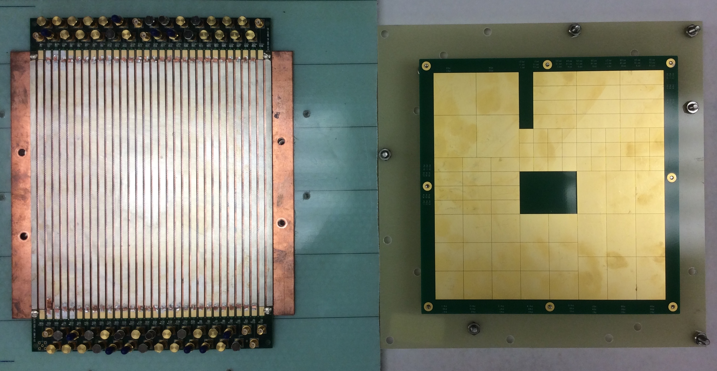
The capacitive coupling configuration enables using a pixelated 2-dimensional array of pads without brazed pins penetrating the ceramic package. A test pickup card, shown in the right-hand panel of Figure 3, consists of a custom printed circuit board with three sizes of square copper pads: 1.27 cm 1.27 cm, 2.54 cm 2.54 cm, and 3.81 cm 3.81 cm. The back side of the board supplies signal ground through which each pad connects to an SMA connector.
3 Laser Test Stand
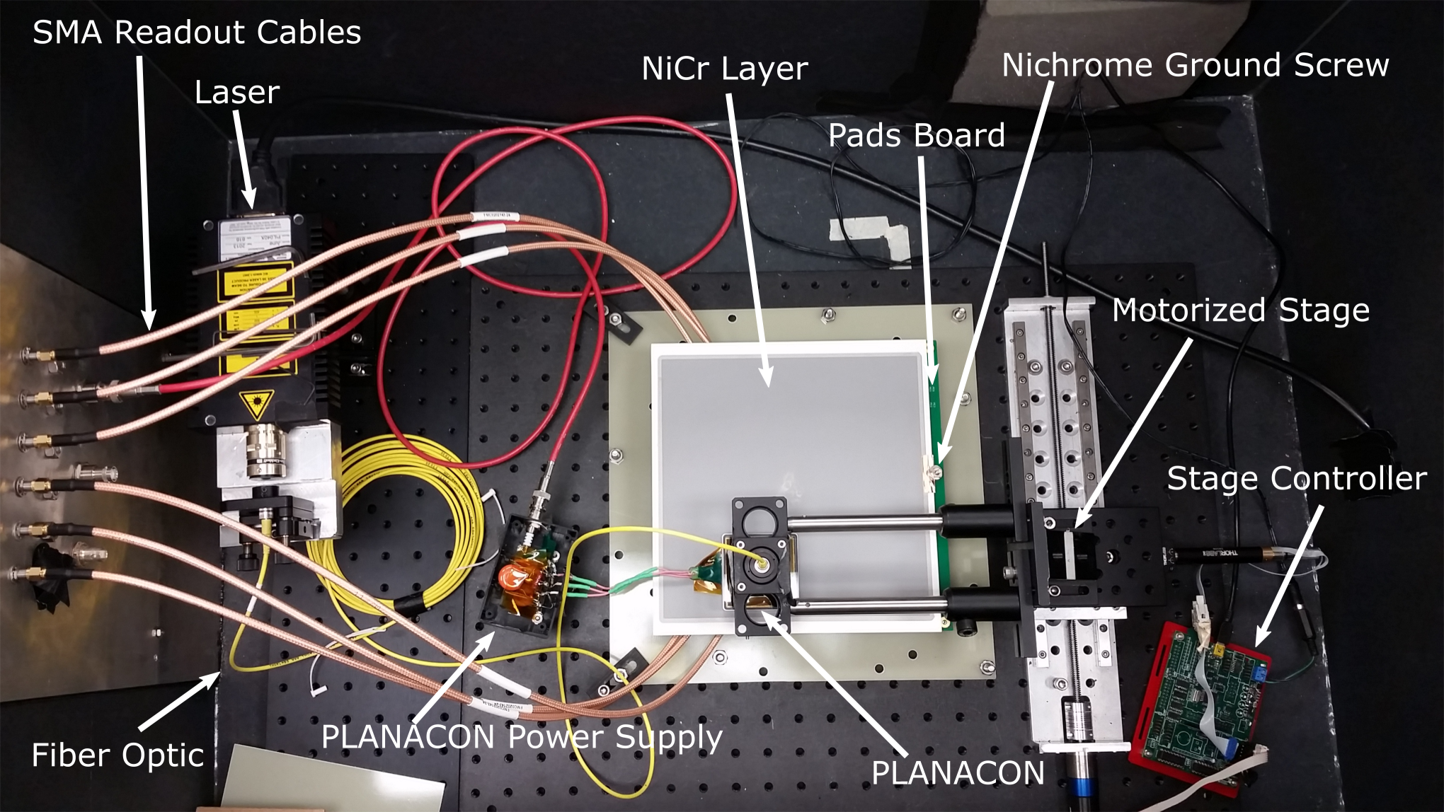
Anodes were tested in both a ‘direct’ configuration, in which one or more individual conducting strips or pads of the signal pickup were electrically connected to the signal source, and the capacitive configuration, in which the signal source was connected to the NiCr film anode and capacitively coupled to the pickup. The signal source consists of a commercial Planacon MCP-PMT [8], illuminated by a 405 nm Pilas laser [22] fed through a fiber optic. The fiber is attached to a remotely-controlled translation stage to the window, as shown in Figure 4. The translation stage is equipped with remote control PID motor drivers that allow for position scans with a fiber position uncertainty of 1 mm [23]. The Planacon is coupled to the 10-nm-thick NiCr anode film evaporated on a 3-mm-thick ceramic substrate with uncured silver epoxy.
3.1 Source of MCP generated pulses
Previous tests of large-area microstrip performance have been performed using MCP-PMT pulses generated by a Ti-Saph laser in a pumped vacuum test facility [2, 24], or on a stand-alone anode in air with a fast pulse generator and a spectrum analyzer [6]. Here, for convenience and compatibility with the dark box, a commercial Planacon MCP-PMT [8] is used as the source of MCP pulses.
3.2 Electrical Connections
High voltage is distributed to the Planacon photocathode, the top, and the bottom of the 2-MCP amplification stage via an external 50 M resistive divider [25], with a return from the anode to HV ground through 2k. The Planacon was typically operated at a voltage of 1700 V.
The Planacon internal anode consists of an internal array of 32 32 metal pads that penetrate the vacuum packaging. An area of 13 cm2 of the bottom of the Planacon was connected to the readout board using a consistent volume of uncured silver epoxy [26]. The epoxy provides a resistive path to ground for the collected charge, and a capacitive high-frequency connection to the signal readout. The resistance of the paste connection was small compared to the resistance of the HV divider string so that the anode-DC offset was measured to be negligible.
For the direct-coupling tests, the silver paste connects the Planacon anode pads to the signal pickup board. The signals are transmitted to the front-end electronics via 50 cables.
For the capacitive coupling tests, the Planacon anode pads are instead connected via silver paste to the NiCr film on the top surface of the ceramic substrate. The pickup board is located directly under the ceramic substrate, as shown in Figure 1. The signal connection to the front-end electronics is the same as for the direct coupling case.
The effective impedance across which the signal current generates a voltage depends on the geometry of the pickup. The strip-line pickup has each end of the strips terminated with 50, and there is substantial cross-talk between the strips [6]. The effect of the 10-nm-Nicr anode is to spread the signal laterally among strips (see Section 4.2.1); the effective impedance to signal ground is thus substantially lower than 50.
3.3 Readout Electronics and Data Acquisition
The readout electronics system was based on the PSEC4 fast waveform digitization Application Specific Integrated Circuit (ASIC), a custom, 6-channel waveform digitizer that samples at 10-15 GSamples/sec [27]. The PSEC4 is available as a stand-alone single-chip system with FPGA local control, read out by a laptop computer via USB. A calibrated PSEC4 waveform digitizer has an analog bandwidth of 1.5 GHz and a typical RMS noise level of 700 V [27]. The tests in this paper, done on an uncalibrated chip in a noisy environment, have a measured noise level of 2.2 mV, to be compared with the 50 - 300mV of the typical Planacon signals.
4 Results
4.1 Rise-Time and Amplitude Comparison
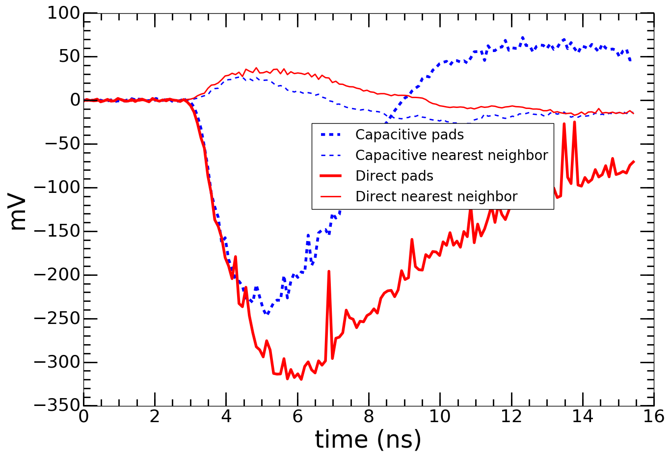
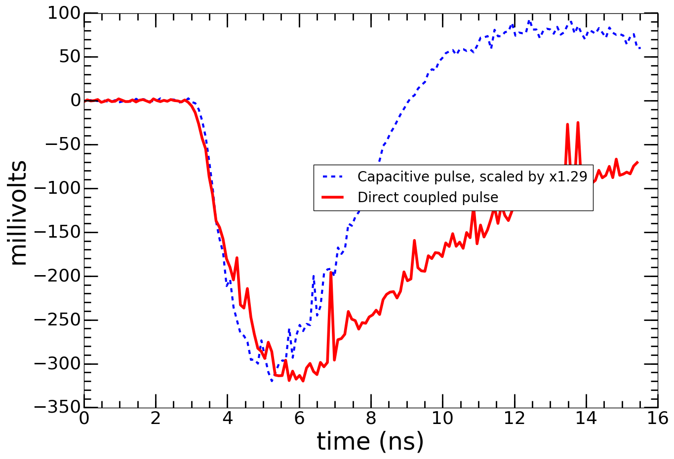
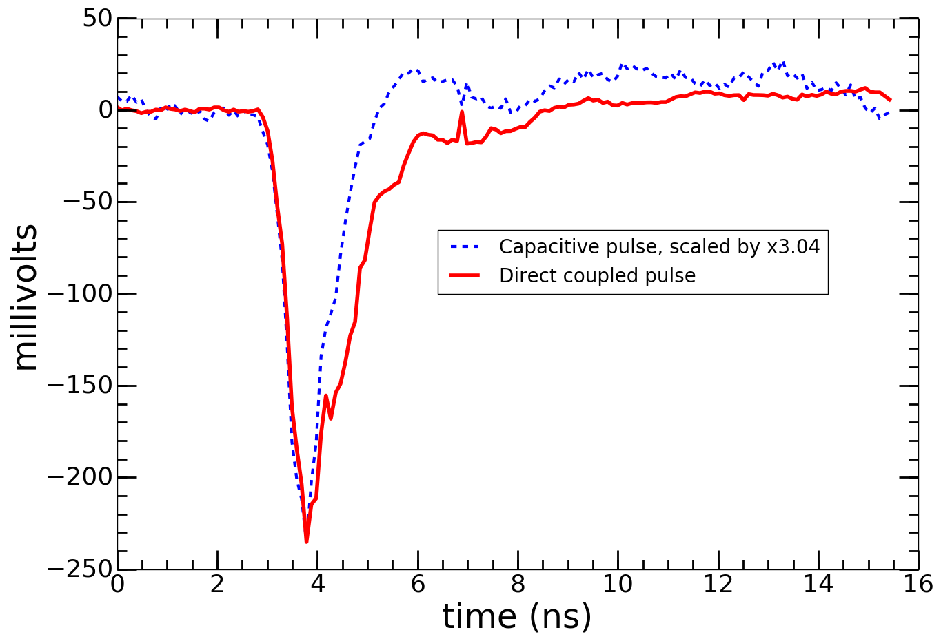
Figure 5 shows typical individual pulses recorded by the test system. The panels in the upper row show a direct pulse (red solid line) and a capacitively coupled pulse (blue, dashed line) for the 2.54 cm 2.54 cm pad configuration. The right-hand panel shows the capacitively coupled pulses normalized to the largest direct pulse. Approximately 80% of the direct amplitude is picked up by one pad in the capacitive geometry, with no degradation in risetime.
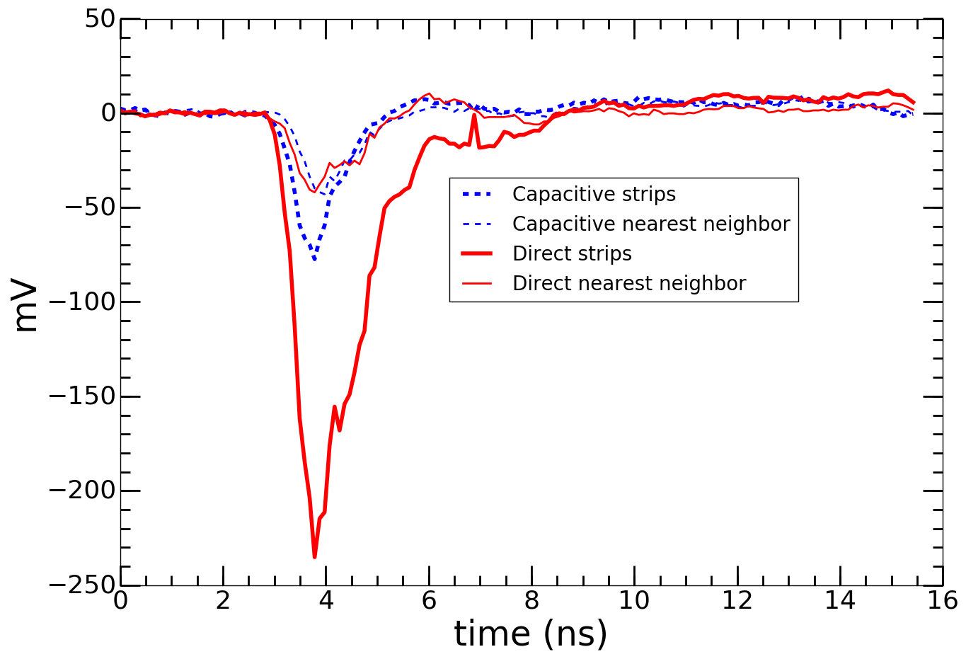
The two panels in the lower row show the same comparison for the micro-strip pickup configuration. In the capacitive case, shown in the left-hand panel, 34% of the direct amplitude is measured on the strip directly under the laser, and substantial portions of the amplitude are recorded on neighboring strips. The right-hand panel shows the direct and capacitive pulses normalized by amplitude; the rise times and pulse widths are essentially identical. The comparison between the top and bottom rows shows the inherently higher bandwidth of the RF micro-strips versus the two-dimensional geometry of the pads.
4.2 Cross-Talk and Position resolution
The physical placement of the ceramic substrate between the NiCr anode and the pickup electrodes spreads the signal, and thus changes the spatial resolution and coupling between neighboring pickup electrodes. Each electrode is separately digitized so in principle no signal is lost as long as each signal is large compared to the single-channel noise. The ‘cross-talk’ between neighboring electrodes allows for spatial resolution better than the strip pitch. However, cross-talk can present problems for pattern recognition in high-occupancy applications [28].
4.2.1 Micro-strip pickup
The micro-strip signal pickup used here is identical in construction to that of Ref. [6], in which the anode was excited directly by LAPPD MCPs. Crosstalk between neighboring micro-strips was used to measure a spatial resolution of 700 m by interpolation [6].
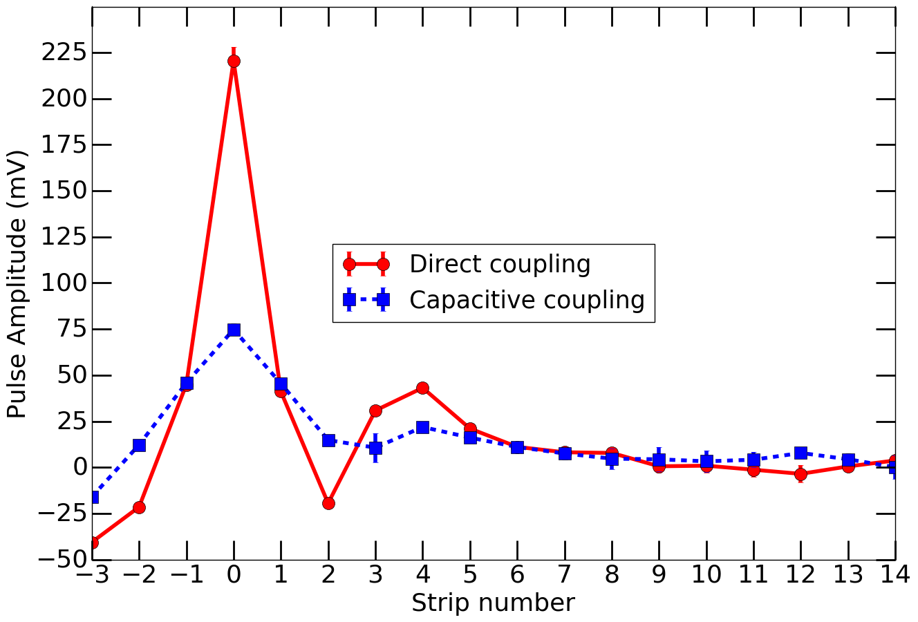
A comparison of the distributions in pulse amplitude on each strip for the directly coupled (red solid line) and capacitively coupled (blue dashed line) configurations is shown in Figure 6. Relative to the directly coupled configuration, the signal is spread to neighboring strips, and the amplitude on the central strip-line is 66% smaller. We attribute this effect to the intervening extended NiCr film, distributing the current laterally, and forming a lower impedance coupling to the pickup strips below.
4.2.2 Pad-array pickup
The optimal size of the pads in the signal pickup is application-specific, and depends on the desired spatial resolution and expected occupancy. For example, a large neutrino detector deep underground will be characterized by low rate and typically low occupancy, with a resolution that depends on size and analysis technique [29]. In contrast, a detector at a high-energy hadron collider will typically have very high occupancy, and a resolution that depends on the specific use, such as time-of-flight for charged particles [30] or calorimetry [31]. The ease of changing the pad size allows accommodation of varying rate or resolution requirements even in a single application, for example changing the pad size as a function of rapidity at a collider detector.
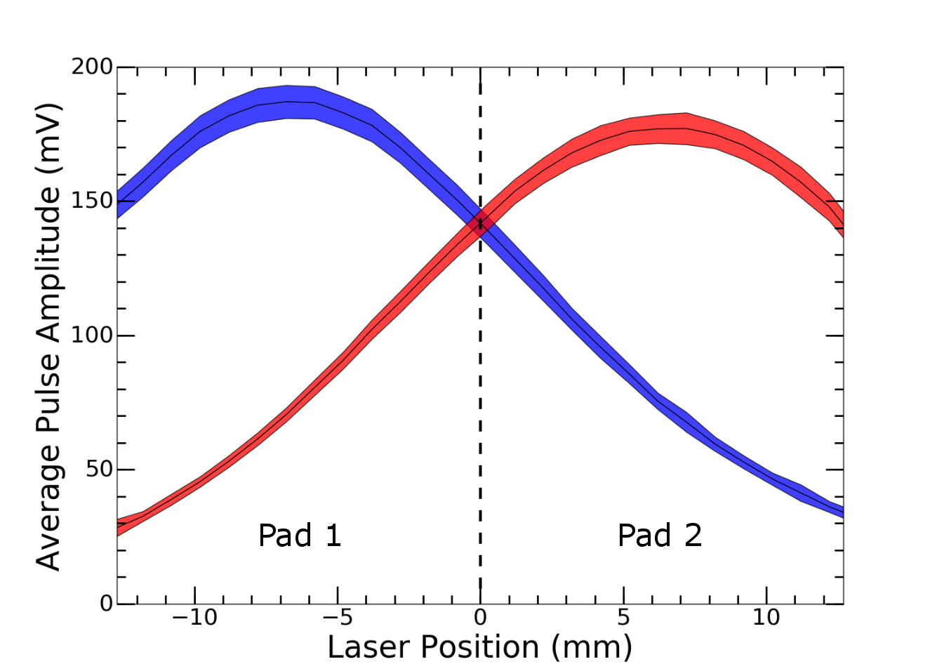
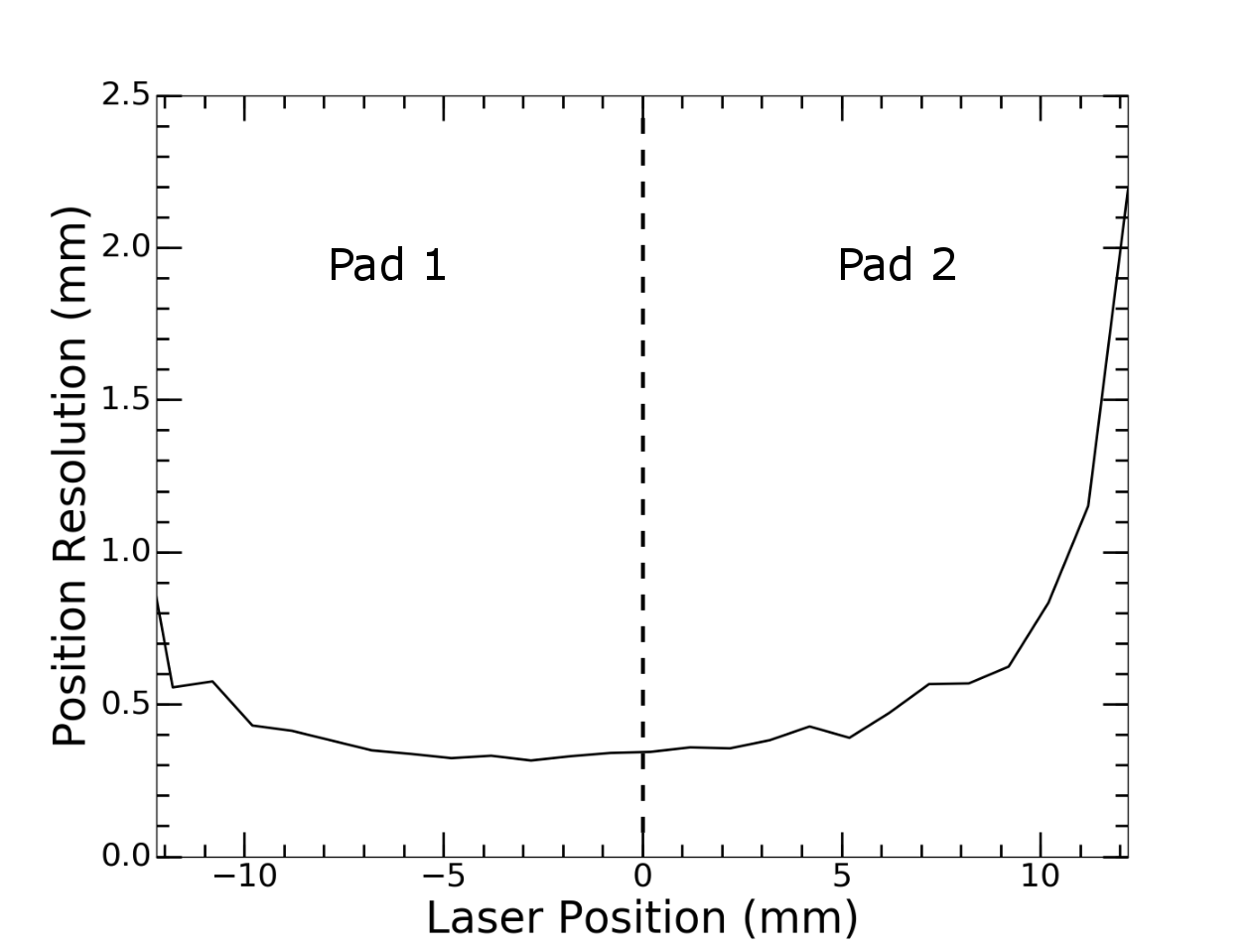
The test pad signal pickup board was constructed with pads of different sizes, motivated by the range needed for high-luminosity collider applications. The results on position resolution are measured by scanning the laser fiber position over a 30 mm range along an array of 1.27 cm pads.
The left-hand panel of Figure 7 shows the signal amplitude on two 1.27 cm pads as a function of laser position as the laser is scanned across their interface. The right-hand panel shows the position resolution calculated from the fraction , where is the amplitude on the first pad, and is the amplitude on the second pad. The resolution is slowly-varying as long as the laser signal is shared between the two pads, sharply rising when only one pad contains the signal, and has a minimum of 315 m when the laser is centered on the interface.
5 Conclusions
We have tested a 20 20 cm2 thin-metal-film internal anode capacitively coupled to an array of signal pads or micro-strips for use in fast microchannel-plate photomultipliers . The pads or micro-strips constituting the signal pickup are located on a plane that can be put in close proximity to the bottom outer surface of the sealed photodetector, with no electrical connections through the photodetector hermetic vacuum package other than a single ground connection to the internal anode.
The tests were performed with a Planacon MCP-PMT excited by a Pilas laser as the signal source. For the capacitively coupled configuration, the Planacon was coupled electrically to the test anode plane, which consisted of a 10-nm-thick NiCr film deposited on a 96-percent-pure Al2O3 3-mm-thick ceramic plate. The test anode was connected to HV ground through 2k. On the lower side of the ceramic plate, signals were picked up by a plane with signal electrodes on the top surface and a continuous signal ground on the bottom surface. Two signal-pickup readout patterns were tested: 1) parallel 50 25-cm-long micro-strips with an analog bandwidth of 1.5 GHz, and 2) a 20 20 cm2 array of 2-dimensional square pads with sides of 1.27 cm or 2.54 cm. Signals were digitized with a PSEC4 10 GSa/s waveform sampling system.
The results were compared with those obtained with the Planacon directly coupled to the signal pickup planes. The capacitive coupling has no effect on the measured rise-time of the pulse for both the pad and micro-strip pickup geometries, preserving the analog bandwidth for timing resolution. For capacitively coupled pads of 2.54 cm 2.54 cm , we observe 80% of the directly coupled amplitude. For the micro-strip pattern, we measure 34% of the directly coupled signal on the strip with the largest signal, still large enough for precision spatial measurements. We attribute the loss on the excited strip to a lower impedance to signal ground due to crosstalk with multiple micro-strips, each terminated at both ends in 50.
Cross-talk between neighboring electrodes on the signal pickup card allows spatial resolution more precise than the size of the individual electrodes. Scanning with a translation stage, we find that on 1.27 cm 1.27 cm pads, position resolution is nearly constant over a region in which there is signal sharing between 2 neighboring pads, with an optimal resolution of 315 m.
6 Acknowledgments
The activities at the University of Chicago were supported by the Department of Energy under DE-SC-0008172 and the National Science Foundation under grant PHY-1066014. We owe many thanks to E. Oberla for help with the PSEC4-based electronics readout. We thank F. Tang (UC Electronics Design Group) for designing the pad signal pickup card; C. Craven, M. Foley, M. J. Minot (Incom, Inc) and B. Shi (Thin Film Deposition Lab, Argonne APS) for the deposition of thin metal films on the ceramic anode planes; J. DeFazio (Photonis, Inc) for support of the Planacon photodetector; and R. Northrop (UC Engineering Center) and M. Heintz (UC EDG) for essential mechanical engineering and computational support.
References
References
- [1] J.L. Wiza, Micro-channel Plate Detectors. Nuclear Instruments and Methods 162, 1979, pp 587-601
- [2] B.W. Adams, A. Elagin, H. Frisch, R. Obaid, E. Oberla, A. Vostrikov, R. Wagner, J. Wang, M. Wetstein; Timing Characteristics of Large Area Picosecond Photodetectors; Nucl. Inst. Meth. Phys. Res. A. , Vol. 795, pp 1-11 (Sept. 2015);
- [3] O.H.W. Siegmund, J.B. McPhate, J.V. Vallerga, A.S. Tremsin, H. Frisch, J. Elam, A. Mane, and R. Wagner; Large Area Event Counting Detectors with High Spatial and Temporal Resolution, JINST 9 C04002, pp. 1748-0221; April 2014
- [4] O. H. W. Siegmund, M. A. Gummin, J. M. Stock, D. R. Marsh, R. Raffanti, J. S. Hull; High-resolution monolithic delay-line readout techniques for two-dimensional microchannel plate detectors; Proc. SPIE 2006, EUV, X-Ray, and Gamma-Ray Instrumentation for Astronomy IV, 176 (Nov. 1993)
- [5] F. Tang, C. Ertley, J.-F. Genat, J. Anderson, K. Byrum, G. Drake, E. May, and G. Sellberg Transmission-Line Readout with Good Time and Space Resolutions for Planacon MCP-PMTs, in Topical Workshop on Electronics for Particle Physics, CERN, pp. 579-583, 2008
- [6] H. Grabas, R. Obaid, E. Oberla, H. Frisch J.-F. Genat, R. Northrop, F. Tang, D. McGinnis, B. Adams, and M. Wetstein RF Strip-line Anodes for Psec Large-area MCP-based Photodetectors, Nucl. Instr. Meth. A71, pp124-131, May 2013
- [7] K. Inami, N. Kishimoto, Y. Enari, M. Nagamine, and T. Ohshima; A 5-ps Tof-counter with an MCP-PMT; Nucl. Instr. Meth. A560, p.303, 2006
-
[8]
Photonis, PlanaconTM; see the Planacon link at
http://www.photonis.com/en/product/. - [9] O. Jagutzki, J. Barnstedt U. Spillmann, L. Spielberger, V. Mergel, K. Ullmann-Pfleger, M. Grewing, and H. W. Schmidt-Boecking; Fast-position and time-sensitive readout of image intensifiers for single-photon detection, Proc. SPIE 3764, p61 (1999)
- [10] O. Jagutzki, A. Czasch, and S. Schössler; Performance of a compact position-sensitive photon counting detector with image charge coupling to an air-side anode, Proc. SPIE 8727, 87270T-87270T-12 (2013)
- [11] J. S. Lapington, J. R. Howorth and J. S. Milnes, J. S.; A reconfigurable image tube using an external electronic image readout, Proc. SPIE 5881, 588109 (2014)
- [12] O. Jagutzki, A. Cerezo, A. Czasch, R. Dorner, M. Hattas, Min Huang, V. Mergel, U. Spillmann, K. Ullmann-Pfleger, T. Weber, H. Schmidt-Bocking, G. D. W. Smith; Multiple hit readout of a microchannel plate detector with a three-layer delay-line anode; in IEEE Transactions on Nuclear Science, 49, 2477; 2002
- [13] J. S. Lapington, J. R. Howorth, and J. S. Milnes; Demountable readout technologies for optical image intensifiers, NIM A573, 243 (2007)
- [14] G. Battistoni, E. Iarocci, G. Nicoletti and L. Trasatti; Detection of induced pulses in proportional wire devices with resistive cathodes; Nucl. Instr. and Meth. 152, 2, 423 (1978)
- [15] A. Czasch, V. Dangendorf, M. Volker, J. Milnes, S. Schössler, R. Lauck, U. Spillmann, J. Howorth, and O. Jagutzki; Position and time sensitive photon counting detector with image charge delay-line readout, Proc. SPIE 6771, 67710W-67710W-12 (2007)
-
[16]
RoentDek Handels GmbH, Kelkheim, Germany;
see http://www.roentdek.com/detectors/. - [17] Incom Inc. Charlton Mass. See http://www.incomusa.com/
- [18] B. Adams et al.; A Brief Technical History of the Large-Area Picosecond Photodetector (LAPPD) Collaboration; Submitted to World Scientific Aug. 2016
- [19] Due to availability of ceramic plates in stock the test anode is 3-mm-thick; the base of the MCP-PMT is 5mm thick.
- [20] NiCrA; 80:20% Nickel:Chrome by weight.
- [21] Coorstek AD-96; Coorstek, Golden Co. 80403
- [22] Pilas EIG 1000D with 405 nm head; Advanced Laser Diode Systems, Berlin, Germany.
- [23] Dragonfly Devices; see www.dragonflydevices.com
- [24] B. Adams, M. Chollet, A. Elagin, A. Vostrikov, M. Wetstein, R. Obaid, and P. Webster A Test-facility for Large-Area Microchannel Plate Detector Assemblies using a Pulsed Sub-picosecond Laser Review of Scientific Instruments 84, 061301 (2013)
- [25] E. Oberla, Charged Particle Tracking in a Water Cherenkov Optical Time Projection Chamber, Ph.D Dissertation, University of Chicago, Aug. 2015
- [26] Transene Silver Bond 50 Epoxy Paste; Transene Co., Inc.; Danvers MA 01923
- [27] E. Oberla, J.-F. Genat, H. Grabas, H. Frisch, K. Nishimura, and G Varner A 15 GSa/s, 1.5 GHz Bandwidth Waveform Digitizing ASIC, Nucl. Instr. Meth. A735, 21 Jan., 2014, 452;
- [28] G. R. Jocher, M. J. Wetstein, B. W. Adams, K. Nishimura, S. M. Usman; Multiple-photon disambiguation on stripline-anode Micro-Channel Plates; Nuclear Inst. and Methods in Physics Research, A, Volume 822,p 25, (June 2016)
- [29] C. Aberle, A. Elagin, H.J. Frisch, M. Wetstein, L. Winslow. Measuring Directionality in Double-Beta Decay and Neutrino Interactions with Kiloton-Scale Scintillation Detectors; Journal of Instrumentation Volume 9 (June 2014) JINST 9 P06012 doi:10.1088/1748-0221/9/06/P06012 e-Print arXiv:1307.5813
- [30] T. Credo, H. Frisch, H. Sanders, R. Schroll, and F. Tang; Picosecond Time-of-Flight Measurement for Colliders Using Cherenkov Light Proceedings of the IEEE, Rome, Italy, Oct. 2004; Nuclear Science Symposium Conference Record, 2004 IEEE, Volume 1.
-
[31]
See, for example: A. Apresyan, , S. Los,
C. Pena, F. Presutti, A. Ronzhin, M. Spiropulu, S. Xie; Direct
tests of a pixelated microchannel plate as the active element of a
shower maximum detector; Nucl. Instr. and Meth A828, (1 August 2016);
S. N. White; R&D for a Dedicated Fast Timing Layer in the CMS Endcap Upgrade arXiv:1409.1165;