Electronic transport in disordered MoS2 nanoribbons
Abstract
We study the electronic structure and transport properties of zigzag and armchair monolayer molybdenum disulfide nanoribbons using an 11-band tight-binding model that accurately reproduces the material’s bulk band structure near the band gap. We study the electronic properties of pristine zigzag and armchair nanoribbons, paying particular attention to the edges states that appear within the MoS2 bulk gap. By analyzing both their orbital composition and their local density of states, we find that in zigzag-terminated nanoribbons these states can be localized at a single edge for certain energies independent of the nanoribbon width. We also study the effects of disorder in these systems using the recursive Green’s function technique. We show that for the zigzag nanoribbons, the conductance due to the edge states is strongly suppressed by short-range disorder such as vacancies. In contrast, the local density of states still shows edge localization. We also show that long-range disorder has a small effect on the transport properties of nanoribbons within the bulk gap energy window.
pacs:
72.10.-d,72.80.Ga,73.23.-b,73.63.-bI Introduction
The wide interest in graphene has triggered an intense investigation of the electronic and mechanical properties of other two-dimensional materials [1, 2, 3]. Among them, transition metal dichalcogenides (TMDs), and particularly molybdenum disulfide (MoS2), are of great appeal due to their finite band gap which could be explored for optoelectronic applications [1]. Understanding the reasons behind the poor mobility of the present-day state-of-the-art TMD samples is a subject of intense theoretical and experimental debate [4, 5, 6, 7, 8, 9, 10] and a challenge for future practical uses of these materials in devices.
Impressive advances in sample production have been reported. Molybdenum disulfide nanowires and nanoribbons with subnanometer width have been recently synthesized, with good quality edges, mostly zigzag terminated [11, 12, 13, 14, 15]. While great progress has been made on the experimental side, the theoretical understanding of the properties of these systems is still very limited. The theoretical literature consists mainly of density functional theory (DFT) studies [16, 17, 13, 18, 19, 20, 21, 22, 23, 24, 25, 26, 27] that address only the electronic structure of pristine and narrow TMD nanoribbons.
As in graphene, the presence of edges dramatically modifies the low-energy spectrum of TMDs. DFT studies of MoS2 find very distinct features in the band structure of nanoribbons as compared with the bulk: MoS2 nanoribbons can be metallic depending on the orientation of the edges. Zigzag nanoribbons typically show ferromagnetic and metallic behavior, irrespective of their width, thickness, and passivation [16, 17, 13, 18, 19]. By increasing the nanoribbon width, it was found that the metallic edge state bands are preserved, remaining as gap states (inside the bulk gap) but ferromagnetism is rapidly suppressed [16]. In contrast, Refs. [20] and [21] predict a semiconductor (- or -type) or half-metallic behavior depending on the nanoribbon zigzag edge saturation. Most studies [13, 18, 24, 22, 23, 16, 20] find that armchair nanoribbons are nonmagnetic and semiconducting. To the best of our knowledge, the only exception is Ref. [17], which reports metallic armchair nanoribbons with a magnetic moment depending on the passivation condition.
Although insightful, these results cannot be directly used to model realistic TMD nanoribbons. The computational cost of DFT does not allow one to address nanoribbons with realistic sizes or disorder, a ubiquitous feature in systems synthesized these days. To account for these limitations, one needs a computationally more efficient model that accurately describes the MoS2 low-energy bands and that is suitable for a disorder modeling at the atomistic scale. To study disorder effects in TMD nanoribbons, in this paper we consider a tight-binding model. Due to its single-particle nature, the tight-binding Hamiltonian does not describe the magnetic features of the nanoribbon edge states. On the other hand, we recall that the edge magnetization similar to TMDs has been extensively theoretically studied in pristine graphene nanoribbons [28, 29]. The effect remains elusive to experiments and has been observed only indirectly [30], possibly because edge disorder quenches magnetic properties [31].
One of the most used tight-binding implementations for MoS2 [27] uses only the orbitals of Mo. Hence, sulfur vacancies, one of the most important sources of disorder, cannot be described by this model. A recent paper [32] uses an 11-band model to study the electronic band structure of ribbons with about 30 nm of width. Reference [32] finds that nanoribbons with zigzag edges are metallic, with edge states that close the bulk gap energy region, while nanoribbons with armchair edges are semiconductors. This is in line with recent scanning tunneling microscopy (STM) spectroscopy results [33, 15] that report the occurrence of a metallic phase within the bulk gap at the (zigzag) edges of a MoS2 monolayer on graphite. Similar results have been also reported for MoS2 on epitaxial graphene [34]. These experimental observations suggest that the metallic edge modes are robust to disorder.
In this paper we use the tight-binding model put forward in Ref. [35] to systematically study the electronic properties of monolayer MoS2 nanoribbons. Our calculations reproduce qualitatively the band structure of narrow nanoribbons obtained by DFT. We show the necessity of considering the full Hamiltonian, with even and odd parities with respect to -axis reflection, for an accurate description of nanoribbon electronic states within the bulk gap energy window. By doing so, we observe the appearance of an odd-parity band close to the Fermi level for both kinds of edge terminations. In the zigzag case, we analyze the edge nature of states inside the bulk gap. Interestingly, we find that the metallic bands correspond to states localized at a single edge independent of nanoribbon width and disorder.
We also study the conductance and local density of states (LDOS) of both pristine and disordered MoS2 zigzag and pristine armchair nanoribbons using the recursive Green’s function method. We focus our attention on the effect of short and long-range disorder on the conductance of zigzag nanoribbons. The results are interpreted in terms of topological invariants and their robust protection against disorder. We find that even a modest concentration of vacancies close to the edges can cause a large transmission suppression, particularly within the bulk gap energy window. In contrast, long-range scattering does not have a significant effect on the conductance.
The paper is organized as follows. In Sec. II we present the theoretical model and the band-structure calculations for pristine MoS2 nanoribbons with zigzag and armchair edges. In Sec. III we discuss the electronic transport in clean and disordered nanoribbons with Fermi energy in the vicinity of the bulk gap. First, in Sec. III.1 we analyze the conductance of pristine zigzag and armchair nanoribbons, supplemented by a discussion of the LDOS of the zigzag case. Second, in Sec. III.2 we study the effect of both short- and long-range disorder in the transmission and the LDOS of zigzag nanoribbons. Finally, we draw some conclusions in Sec. IV.
II Band structure of pristine nanoribbons
In this section we present the band-structure calculations for MoS2 nanoribbons for both armchair and zigzag edges using the tight-binding model introduced in Ref. [35].
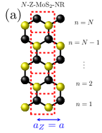
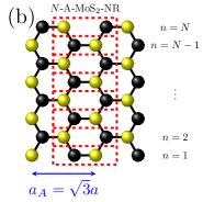
Figure 1 shows the different kinds of MoS2 nanoribbon unit cells considered in this paper and serves a guide for the notation. We consider zigzag (Z-MoS2-NR) and armchair MoS2 nanoribbons (A-MoS2-NR) with translational invariance along the “horizontal” direction and a finite width along its “vertical” direction. Figure 1 shows the ribbons from a top view, where two sulfur (S), one above and one below the plane containing the molybdenum (Mo) atoms, sit on top of each other. For notation convenience, we identify ribbons with different widths as -Z-MoS2-NR and -A-MoS2-NR, where the integer corresponds to the number of zigzag lines and the number of armchair dimers, respectively, indicated by the dashed rectangles [36]. Each Mo (S) atom contains five (three) orbitals corresponding, in the limit , to a bulk MoS2 unit cell with three atoms (one Mo and two S) with a total of orbitals [35]. Since both zigzag lines and armchair dimers have one Mo and two S atoms, the total number of orbitals in any ribbon is . We define the zigzag and armchair lattice parameters as and , respectively, where Å is the Mo-Mo distance.
As discussed in Ref. [35], the full model Hamiltonian for the MoS2 monolayer can be decoupled into odd and even symmetry parts with respect to the Mo plane ( symmetry). For a MoS2 monolayer, the orbital compositions of the valence band and the conduction band are mostly even [35, 32]. In Ref. [32], the authors take advantage of this fact and compute the band structure of MoS2 nanoribbons using only the even part of the Hamiltonian, asserting that odd parity bands are energetically far away from the bulk gap. Unfortunately that is not the case for MoS2 nanoribbons, as we show in the following.
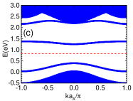
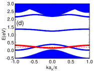
Due to finite-size effects, the band structure of MoS2 nanoribbons can be significantly different from that of bulk monolayers. The bands suffer reorganization and/or hybridization which can enhance the contribution of the odd symmetry bands in the bulk gap region. For this reason we implement the all-band model (ABM), consisting of even and odd symmetry bands, to compute the band structure of Z-MoS2-NR and A-MoS2-NR. Those are compared with the even-band model (EBM). We study ribbons characterized by widths comparable with experimentally produced samples [11, 12, 13, 14, 15].
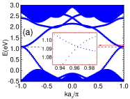
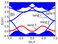
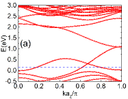
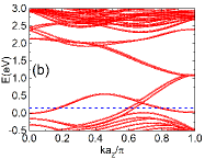
Typical results are shown in Fig. 2. As predicted earlier [32], clean zigzag ribbons are metallic. This applies for both the even- and the all-band models. In contrast, pristine armchair ribbons are semiconductor for the even-band model [32] and metallic when even and odd bands are considered (this work). In neither case do the edge state bands extend over the whole energy window corresponding to the bulk gap above the Fermi level. Consequently, armchair MoS2 nanoribbons with a small electron doping 111Taking spin degeneracy into account, this corresponds to two electrons in excess over the whole nanoribbon area. also become semiconductor in the all-bands model.
The comparison between the two models unravels the presence of an odd band around the energy of eV for both edge orientations, as highlighted in red in Figs. 2(b) and 2(d). We note that in the armchair case the bands in the energy interval eV of Figs. 2(c) and 2(d) are roughly doubly degenerate, while in the zigzag case [Figs. 2(a) and 2(b)] there is no degeneracy.
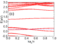
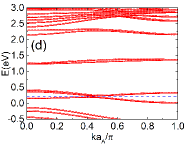
A quantitative comparison between tight-binding and DFT band structure calculations for nanoribbons is difficult, since most DFT studies assume edge passivation conditions which are not included in the tight-binding model. Moreover, DFT accounts for electron-electron interactions due to the non-homogeneous charge distribution at the vicinity of the nanoribbon edges. Nonetheless, the band structures we obtain show good qualitative and quantitative agreement with results from the DFT literature [13, 16, 24, 25, 26, 17, 22, 18, 27, 23, 20, 21]. The comparison with the band structure presented in Ref. [38] for zigzag nanoribbons where the authors find a band very similar to our “odd band” is particularly reassuring.
The band structures presented so far are not spin resolved. We include spin resolution following the prescription reported in Ref. [35]. We consider the all-band model with orbitals per bulk unit cell and introduce the spin-orbit coupling term . Here, is the intrinsic atomic spin-orbit strength for Mo or S, is the atomic orbital angular momentum operator, and is the electronic spin operator acting on all atoms of the system. We set the parameters meV and meV [35, 39], which reproduce the experimental spin splitting at the point of the bulk MoS2 valence band [40].
In Fig. 3 we show the band structure for zigzag and armchair MoS2 nanoribbons with and without the spin-orbit interaction in the energy window of interest. The spin-resolved bands of the 10-Z-MoS2-NR and the 10-A-MoS2-NR in Figs. 3(b) and Fig. 3(d), respectively, show that the main bands in the interval eV present very small spin splittings. (For some bands the effect is hard to notice within the resolution of the figures.) We use the full spin-orbit coupling Hamiltonian, including both spin-conserving and spin-flipping terms. We have verified that the spin-splitting effect on the band structure is due to the diagonal (spin-conserving) terms of the Hamiltonian, while off-diagonal (spin-flipping) terms give a negligible contribution. In the bulk region, for energies eV and eV, the spin splitting is more pronounced. We find that including spin-orbit coupling in our all-band model provides a spin splitting in the armchair band structure in Fig. 3(d) which is not found in Ref. [32].
The small energy splitting of the spin-resolved bands suggests that we can safely neglect the intra-atomic spin-orbit coupling and treat the system as spin degenerate when addressing transport properties.
Let us now focus our discussion on the orbital character of the metallic bands of zigzag nanoribbons in Fig. 2(b). Reference [32] established the edge nature of two of the even bands inside the gap (corresponding to bands 1 and 2 in Fig. 2) and the delocalized nature of the valence and conduction bands by plotting their wave functions across the ribbon width. In our model, bands and touch each other very close to the Brillouin zone (BZ) edge at , close to the bulk and points, having an energy difference of roughly meV at the BZ edge. Those features are nearly imperceptible in Fig. 2(b). In Ref. [32] the bands cross further away from the BZ edge, at , forming one-dimensional analogs of Dirac cones [41]. The latter are more pronounced than the ones we obtain, with an energy difference of roughly meV at the BZ edge. We stress that these effects are purely orbital and each band is spin degenerate.
We determine the edge nature of the bands from through in Fig. 2(b) by analyzing their wave functions along the Brillouin zone. By studying the squared wave functions of all atoms in the ribbon unit cell (not shown here), we determine whether a particular state is distributed mostly near the edges (edge state) or across the whole ribbon (bulk state). We find that all midgap states in Fig. 2(b) are localized at the nanoribbon edges. Band is located at the S-terminated edge while bands , and are located at the Mo-terminated edge. We also notice that one of the valence bands at around eV has the same edge nature as the bands , , and (it can be seen in Fig. 6, where a larger energy interval is shown), while other usual bulk bands have Gaussian-like envelopes as noted in Ref. [32].
The appearance of metallic bands in MoS2 ribbons can be interpreted in topological terms. The first classification of the topological properties of a system can be done according to its Chern number [42]. The latter distinguishes a simple insulator, with Chern number equal to zero, from a system with topologically protected edge states, equivalent to a quantum Hall state, where the Chern number is non zero. This classification fails in systems with time-reversal symmetry, since it leads to a zero Chern number even for systems with topologically protected edge states [43, 42]. In these cases, it is customary to use another topological invariant, the invariant, that can be either (strong topological insulator) or (trivial insulator or weak topological insulator) [42].
The zigzag MoS2 ribbon has , since the number of Kramers pairs at a single edge is always even [43, 42] [see Fig. 3(b)]. According to this classification, the system behaves like an ordinary metal, namely, any kind of disorder has a strong effect on the system electronic transport properties.
However, if one considers a single valley and a single spin, the system has a nontrivial topology. Both DFT [32] and tight-binding [32] calculations obtain a large value for the Berry curvature [42] near the and points of MoS2 (bulk) monolayers. The study of the topology around these points [32] shows a non zero Chern number with . Thus, the system has . In other words, instead of the spin texture of a two-dimensional topological insulator, MoS2 nanoribbon edge states exhibit a “valley texture”. This nontrivial bulk-edge correspondence results in the edge band state crossing shown in the inset of Fig. 2(a). The low-energy states of the zigzag MoS2 ribbon around the point, formed by the crossing of bands and (see Fig. 2), behave as a quantum valley Hall state [32]. Hence, in the absence of disorder sources that cause spin-flip transitions, the system is protected against intra valley scattering processes.
Another way of understanding the “local” nature of the protection is under the light of intervalley scattering events [44, 45, 46]. Away from the band crossing energy, states with opposite propagation direction belong to different valleys. Thus, it is only possible to enable backscattering (change the propagation direction) by introducing a disorder source that provides a large enough amount of momentum to scatter the electron state from one valley to the other. Hence, depending on the value of , backscattering can have a large cross section in the presence of short-range scatterers, while as a rule, it is negligible for long-range ones [44, 45, 46]. We study these processes extensively in the following sections.
Before proceeding to the analysis of the transport properties, a comment on different tight-binding parametrizations for MoS2 is in order. A recent study [19] argues that the origin of the metallic states in zigzag nanoribbons is due to polar discontinuities at the edges. That paper reports that DFT calculations give spin-polarized bands closing the bulk gap, while a Wannier tight-binding model leads to edge state bands with a band gap of about 0.3 eV, independent of the nanoribbon width. Based on these results, the authors [19] conclude that metallicity is driven by the electric fields caused by charge polarization at the system edges. In contrast, our tight-binding model (and also that of Ref. [32]) gives metallic edge state bands solely due to geometric effects, since we do not account for electronic interactions. We recall that the tight-binding model we use is not the same as the one of Ref. [19]. In our case, the tight-binding parameters were obtained from an accurate fit of the band energies and orbital compositions of MoS2 bulk DFT calculations [35]. In any event, despite the differences in spin polarization, both models indicate that the edge states remain metallic, closing the bulk gap, irrespective of the nanoribbon width. The understanding of the nature of the discrepancies is still unclear and beyond the scope of this paper, which is the study of disorder effects on the conductance of MoS2 nanoribbons using a state-of-the-art single-particle effective Hamiltonian.
III Transport in pristine and disordered nanoribbons
In this section we study the electronic transport in MoS2 nanoribbons. In the zigzag case, we discuss our findings in light of the closing of the gap by the metallic edge states. We consider the electronic transport in a system composed by a central part connected to two electron reservoirs maintained at different chemical potentials that act as source and drain terminals. The central part is a nanoribbon of width (see Fig. 1) and length , corresponding to the number of longitudinal unit cells (slices). We calculate the Landauer conductance, given in terms of the electronic transmission between the source (left reservoir ) and the drain (right reservoir ), using the Caroli formula [47, 48],
| (1) |
where () is the decay width function of left (right) contact, and () is the retarded (advanced) Green’s function describing the propagation from to (from to ).
We model the contacts as semi-infinite lattices, calculate the level width functions and using the decimation technique [49, 50], and using the recursive Green’s function method (RGF) [51]. This method allows for a numerically efficient computation of the electronic transport properties and spectral properties [50] such as the local density of states, namely
| (2) |
Here, labels the orbital inside the atom . It also allows for an amenable inclusion of several disorder mechanisms at the microscopic level [50].
In the following we present our numerical calculations of the electronic transmission and LDOS for pristine nanoribbons and for zigzag nanoribbons with defects.
III.1 Pristine zigzag and armchair nanoribbons
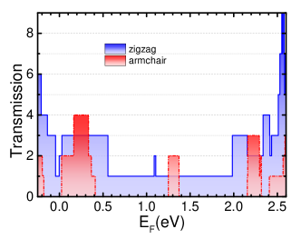
In Fig. 4, we present the transmission for pristine MoS2 nanoribbons. The results correspond to nanoribbons of widths comparable to the ones considered in the band-structure DFT literature [13, 16, 24, 25, 26, 17, 22, 18, 27, 23, 20]. We note that these nanoribbons have smaller widths than the ones considered in the band-structure study of the previous section. Nonetheless, we have checked that their metallic edge states remain almost invariant with increasing width. Thus, the chosen ribbon width allows for faster computation of the electronic transport quantities and still gives insight on the behavior of the edge modes of the wider ribbons.
Figure 4 shows the pristine ribbon transmission as a function of the Fermi energy . The transmission is quantized and consistent with the number of available energy bands as a function of . As expected, the zigzag edges give origin to metallic edge states (or transmission channels) that make the conductance nonzero over the whole energy interval corresponding to the bulk gap. In contrast, the energy band for nanoribbons with armchair edges splits the transport gap into two smaller ones.
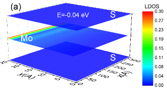
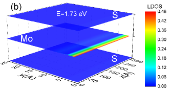
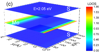
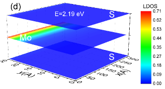
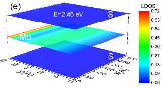
Figure 5 shows the LDOS of the zigzag MoS2 nanoribbon. In the considered geometry, the edge located at is terminated by S atoms while the opposite edge at Å is terminated by Mo atoms, as indicated by the labels in Fig. 5. We find that the orbital composition of all metallic bands is dominated by orbitals located at the Mo layer with a very small LDOS at the S layers. The states are localized at a single nanoribbon’s edge, which we denote according to its termination (either S or Mo). We choose five representative energies on the main plateaus of Fig. 4 corresponding to metallic edge states. The edge states belonging to band in Fig. 5(c) eV are located at the S-terminated edge. The other bands , , and have states mainly distributed at the Mo-terminated edge [see Fig. 5(b) eV and 5(d) eV]. Interestingly, Fig. 5(c) shows a LDOS distributed at both nanoribbon edges, since both bands and contribute to the LDOS at energy eV. Figures 5(a) and 5(e) show the LDOS for eV and eV, respectively. These energies are outside the “bulk energy gap” window, but the corresponding states are still influenced by metallic bands. Due to this fact, the states are mostly localized at the Mo-terminated edge, but a bulk character is manifest.
III.2 Zigzag nanoribbon with defects
Motivated by the topological nature of the metallic bands, we study the robustness of these states around the valleys and against short- and long-range disorder.
Several kinds of defects in MoS2 have been addressed in the literature, such as vacancies, adatoms, substitutional doping, structural and topological defects, folding, wrinkling, and rippling [52]. Among the zero-dimensional defects, the most common are single S vacancies [52]. In this study we also consider double S vacancies and Mo vacancies without reconstruction. As for long-range defects, the most studied ones in MoS2 are ripples [53, 54, 55]. These deform the bonds and modify the interatomic distance of the nanoribbon structure. As a consequence, in a realistic model, the on-site and the hopping parameters of the tight-binding model need to be modified. In addition, electronic charges trapped in the substrate also unavoidably provide a source of local potential disorder. In this paper we address the simple case of local potential scattering for the long-range potential disorder case.
III.2.1 Short-range scattering
Let us study how robust are the edge states in Z-MoS2-NR against short-range disorder, such as vacancies which are ubiquitous in MoS2 [52]. Single and double sulfur (top and bottom) vacancies are the ones with the lowest energy formation [52]. We also consider single Mo vacancies as a model case.
We start with the simplest case of a single short-range defect. We model the defect as a single vacancy by adding a large on-site potential at the lattice atom of interest. We have numerically verified that the large on-site vacancy model is fully equivalent to cutting all the hopping connections between the orbitals of the vacancy atom and the other atoms in the lattice 222We find that this condition is fulfilled for on-site energies of the order of eV..


We perform a systematic study of the effect of a single vacancy on covering all possible vacancy configurations in the nanoribbon unit cell (transverse slice). We consider geometries where the vacancy is equidistant from source and drain contacts to avoid effects due to the coupling to the leads. Here we consider ribbons of width N=. We calculated the conductance for much wider ribbons (N=) for a few cases and obtained very similar results in the gap region, ruling out finite-size effects.
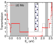
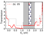
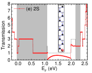
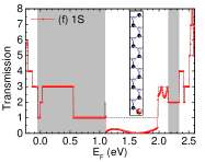
We describe the main findings in Fig. 6. The figure illustrates the effect only for vacancies placed at the nearest edge atomic positions, since we find that the reduction in the transmission becomes progressively smaller as the vacancy is moved away from the nanoribbon edges. We show the transmission for six different vacancy configurations, namely, single S vacancies (top and bottom vacancies are equivalent due to symmetry), double S vacancies (top and bottom planes), and single Mo vacancies near each edge. We recall that eV corresponds to the bulk gap. The gray areas mark the energy intervals of perfect transmission. The corresponding edge states are robust against the presence of vacancies. This can be understood as follows: a vacancy on the Mo-terminated edge, as shown in Figs. 6(a), 6(b), and 6(c), suppresses the transmission of the bands , , and while band remains unaffected with perfect transmission. On the other hand, vacancies on the S-terminated edge strongly suppress the transmission of band and do not affect bands , , and , as seen in Figs. 6(d), 6(e), and 6(f). These results indicate that the propagation of band occurs mainly through the S-terminated edge, while bands , and propagate through the Mo-terminated edge. Note that for eV both bands and are accessible [see Fig. 5(c)] and hence any vacancy configuration near the nanoribbon edges strongly suppresses the transmission. Curiously, Fig. 6 indicates that S di vacancies have a smaller effect on the conductance than S mono vacancies.
In summary, we find that the electronic transport results in the presence of a single vacancy are consistent with the LDOS of the pristine 10-Z-MoS2-NR presented in Fig. 5. Vacancies near the nanoribbon edges dramatically suppress the conductance. Thus, short-range disorder breaks the valley topological protection of the metallic states in zigzag MoS2 nanoribbons. Short-range defects, such as vacancies, enable intervalley scattering processes and hence, backscattering. This reasoning supports the picture that the system behaves like a trivial metal. Are the observations consistent with the robustness of edge states recently experimentally reported in Refs. [33] and [15]? This is the question we address next.
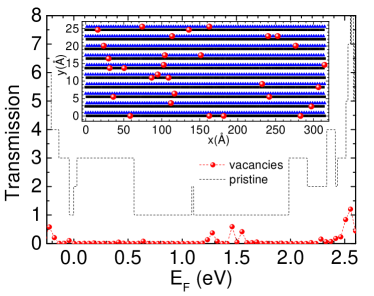
Let us now analyze the electronic transport in a more realistic case by placing random vacancies in the central region. Figure 7 shows the electronic transmission of a disorder realization for a total vacancy concentration (Mo and double S) of for 10-Z-MoS2-NR. As expected, a finite vacancy concentration is extremely detrimental to the electronic transport in the bulk gap energy region. This is a manifestation of Anderson localization in a one-dimensional disordered metal.
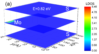
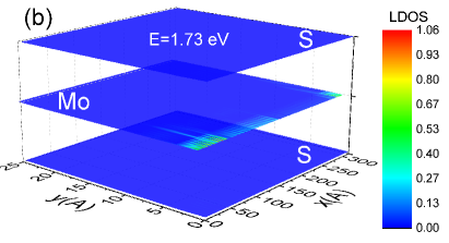
Figure 8 shows the LDOS for the same disorder configuration mentioned above (see Fig. 7). We analyze two selected energies, namely, eV [Fig. 8(a)] and eV [Fig. 8(b)], that correspond to states concentrated at opposite edges. The vacancies near the edges create depletion regions in LDOS, localizing the wave functions and hindering the transport. Surprisingly, we find that the vacancies also induce the appearance of regions with high LDOS at the edges that exceed the maximum LDOS of the pristine system in Fig. 5. We find similar trends for other energies, justifying the wide transport gap ( eV) found in Fig. 7.
III.2.2 Long-range scattering
Let us now consider the case of long-range impurity disorder, which can be caused, for instance, by an inhomogeneous charge distribution in the substrate [57] or by disordered ripples [58]. To study the degree of protection of the edge states against long-range disorder, we place a Gaussian on-site potential centered at , namely,
| (3) |
where and are the impurity strength and range, respectively. Here is taken at one of the system edges and placed equidistantly to the contacts. By varying we can access different scattering range regimes and determine the corresponding effect on the electronic transmission of the system. In graphene deposited on SiO2, the typical rms of is meV [59]. In the absence of a better experimental guidance in the case of MoS2, we take eV.
Let us consider the case of an impurity placed at the S-terminated edge. Figure 9(a) shows the corresponding transmission for three impurity configurations, namely, Å, Å, and Å for eV in a 30-Z-MoS2-NR. We find a nearly perfect transmission quantization for all long-range impurity configurations. We find the same behavior for the impurity at the Mo-terminated edge. In contrast, the shaded areas in Fig. 9(b) indicate the energy windows where the transmission is not perfect, corresponding to edge states localized at the same edge as the impurity center.
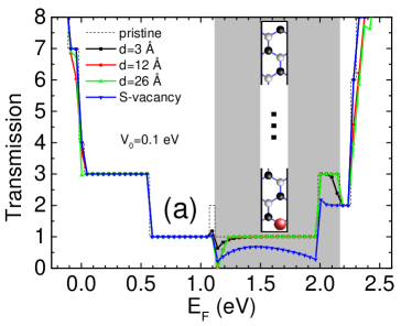
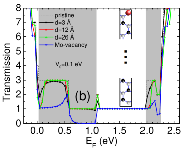
There are also energy windows where we find a stronger suppression of the conductance. For instance, for energies around eV, backscattering processes require a small momentum transfer [see Fig. 2(b)]. As a consequence, long-range impurity enables a transmission suppression as shown in Fig. 9. A similar behavior can be seen at eV, where the band structure allows for several small momentum backscattering processes.
IV Conclusions
In this paper we use the tight-binding model recently proposed by our group [35] to systematically study the electronic structure and transport properties of monolayer MoS2 nanoribbons. Our results reproduce qualitatively the DFT band-structure calculations when limited to narrow and pristine nanoribbons. We argue that it is necessary to consider the full tight-binding Hamiltonian, with even and odd parities, for an accurate description of nanoribbon electronic states within the bulk gap energy window. By doing so, we observe the appearance of an odd-parity band close to the Fermi level at charge neutrality for both kinds of edge terminations. Such bands contribute significantly to the conductance. We analyze the edge nature of the states inside the bulk gap in the zigzag case through the orbital composition of the eigenstates at a given energy and point. Interestingly, we find that the metallic bands correspond to states localized at a single edge independent of the nanoribbon width and disorder, as we explicitly show in our LDOS calculations.
We study the effect of short- and long-range disorder on the conductance and LDOS of zigzag nanoribbons. We find that even a modest concentration of vacancies close to the edges can cause a large transmission suppression, particularly within the bulk gap energy window. In contrast, weak long-range scattering does not have a significant effect on the conductance. We interpret these results in terms of the nature of the metallic bands and their protection against disorder, since the system is robust against intra valley scattering processes. Despite the differences in the calculated band structures, our findings are consistent with the classification of the weak topological insulator proposed in Ref. [32].
In summary, our analysis indicates that short-range defects such as vacancies and edge roughness dramatically suppress the conductance of MoS2 nanoribbons, as they create regions at the edge with negligible LDOS. Surprisingly, there are also regions with enhanced LDOS due to the metallic edge states that are quite robust against disorder. This is consistent with recent scanning tunneling microscopy and spectroscopy experiments that observed a significant localized LDOS at the (rough) edge of a MoS2 sample [33, 15]. To verify that the LDOS is not continuous at the edge and it is not due to adsorbates or molecules, more experimental input is needed.
Acknowledgements.
This work was supported by the Brazilian funding agencies CNPq, CAPES, and FAPERJ. E.M. thanks the Instituto de F\a’isica at Universidade Federal Fluminense for their hospitality.References
- Wang et al. [2012] Q. H. Wang, K. Kalantar-Zadeh, A. Kis, J. N. Coleman, and M. S. Strano, Nature Nanotech. 7, 699 (2012).
- Geim and Grigorieva [2013] A. K. Geim and I. V. Grigorieva, Nature 499, 419 (2013).
- Butler et al. [2013] S. Z. Butler, S. M. Hollen, L. Cao, Y. Cui, J. A. Gupta, H. R. Gutiérrez, T. F. Heinz, S. S. Hong, J. Huang, A. F. Ismach, E. Johnston-Halperin, M. Kuno, V. V. Plashnitsa, R. D. Robinson, R. S. Ruoff, S. Salahuddin, J. Shan, L. Shi, M. G. Spencer, M. Terrones, W. Windl, and J. E. Goldberger, ACS Nano 7, 2898 (2013).
- Qiu et al. [2013] H. Qiu, T. Xu, Z. Wang, W. Ren, H. Nan, Z. Ni, Q. Chen, S. Yuan, F. Miao, F. Song, G. Long, Y. Shi, L. Sun, J. Wang, and X. Wang, Nature Communications 4, 2642 EP (2013).
- Yu et al. [2014] Z. Yu, Y. Pan, Y. Shen, Z. Wang, Z.-Y. Ong, T. Xu, R. Xin, L. Pan, B. Wang, L. Sun, J. Wang, G. Zhang, Y. W. Zhang, Y. Shi, and X. Wang, Nature Communications 5, 5290 EP (2014).
- Radisavljevic and Kis [2013] B. Radisavljevic and A. Kis, Nat. Mater. 12, 815 (2013).
- Schmidt et al. [2014] H. Schmidt, S. Wang, L. Chu, M. Toh, R. Kumar, W. Zhao, A. H. Castro Neto, J. Martin, S. Adam, B. Ozyilmaz, and G. Eda, Nano Letters 14, 1909 (2014).
- Baugher et al. [2013] B. W. H. Baugher, H. O. H. Churchill, Y. Yang, and P. Jarillo-Herrero, Nano Lett. 13, 4212 (2013).
- Zhu et al. [2014] W. Zhu, T. Low, Y.-H. Lee, H. Wang, D. B. Farmer, J. Kong, F. Xia, and P. Avouris, Nature Communications 5, 3087 EP (2014).
- Ghatak et al. [2014] S. Ghatak, S. Mukherjee, M. Jain, D. D. Sarma, and A. Ghosh, “Microscopic origin of charged impurity scattering and flicker noise in mos2 field-effect transistors,” (2014), arXiv:1403.3333 .
- Li et al. [2005] Q. Li, E. C. Walter, W. E. V. D. Veer, B. J. Murray, J. T. Newberg, E. W. Bohannan, J. a. Switzer, J. C. Hemminger, and R. M. Penner, J. Phys. Chem. B 109, 3169 (2005).
- Liu et al. [2013] X. Liu, T. Xu, X. Wu, Z. Zhang, J. Yu, H. Qiu, J.-H. Hong, C.-H. Jin, J.-X. Li, X.-R. Wang, L.-T. Sun, and W. Guo, Nat. Commun. 4, 1776 (2013).
- Wang et al. [2010] Z. Wang, H. Li, Z. Liu, Z. Shi, J. Lu, K. Suenaga, S. K. Joung, T. Okazaki, Z. Gu, J. Zhou, Z. Gao, G. Li, S. Sanvito, E. Wang, and S. Iijima, J. Am. Chem. Soc. 132, 13840 (2010).
- Xu et al. [2016] H. Xu, Z. Ding, C. T. Nai, Y. Bao, F. Cheng, and S. J. R. Tan, Adv. Funct. Mater. 26, 1 (2016).
- Koós et al. [2016] A. A. Koós, P. Vancsó, G. Z. Magda, Z. Osváth, K. Kertész, G. Dobrik, C. Hwang, L. Tapasztó, and L. P. Biró, Carbon 105, 408 (2016).
- Li et al. [2008] Y. Li, Z. Zhou, S. Zhang, and Z. Chen, J. Am. Chem. Soc. 130, 16739 (2008).
- Botello-Méndez et al. [2009] A. R. Botello-Méndez, F. López-Urías, M. Terrones, and H. Terrones, Nanotechnology 20, 325703 (2009).
- Ataca et al. [2011] C. Ataca, H. Şahin, E. Aktuörk, and S. Ciraci, J. Phys. Chem. C 115, 3934 (2011).
- Gibertini and Marzari [2015] M. Gibertini and N. Marzari, Nano Lett. 15, 6229 (2015).
- Pan and Zhang [2012] H. Pan and Y.-W. Zhang, J. Mater. Chem. 22, 7280 (2012).
- Yu and Zheng [2016] S. Yu and W. Zheng, Phys. Chem. Chem. Phys. 18, 4675 (2016).
- Dolui et al. [2012] K. Dolui, C. D. Pemmaraju, and S. Sanvito, ACS Nano 6, 4823 (2012).
- Kim et al. [2015] J. Kim, W. S. Yun, and J. D. Lee, J. Phys. Chem. C 119, 13901 (2015).
- Zhang et al. [2015] L. Zhang, L. Wan, Y. Yu, B. Wang, F. Xu, Y. Wei, and Y. Zhao, J. Phys. Chem. C 119, 22164 (2015).
- Bollinger et al. [2001] M. V. Bollinger, J. V. Lauritsen, K. W. Jacobsen, J. K. Nørskov, S. Helveg, and F. Besenbacher, Phys. Rev. Lett. 87, 196803 (2001).
- Bollinger et al. [2003] M. V. Bollinger, K. W. Jacobsen, and J. K. Nørskov, Phys. Rev. B 67, 085410 (2003).
- Chu et al. [2014] R. L. Chu, G. B. Liu, W. Yao, X. Xu, D. Xiao, and C. Zhang, Phys. Rev. B 89, 155317 (2014).
- Yazyev [2010] O. V. Yazyev, Rep. Prog. Phys. 73, 056501 (2010).
- Carvalho et al. [2014] A. R. Carvalho, J. H. Warnes, and C. H. Lewenkopf, Phys. Rev. B 89, 245444 (2014).
- Tao et al. [2011] C. Tao, L. Jiao, O. V. Yazyev, Y.-C. Chen, J. Feng, X. Zhang, R. B. Capaz, J. M. Tour, A. Zettl, S. G. Louie, H. Dai, and M. F. Crommie, Nature Phys. 7, 616 (2011).
- Wimmer et al. [2008] M. Wimmer, I. Adagideli, S. Berber, D. Tománek, and K. Richter, Phys. Rev. Lett. 100, 177207 (2008).
- Rostami et al. [2016] H. Rostami, R. Asgari, and F. Guinea, Journal of Physics: Condensed Matter 28, 495001 (2016).
- Zhang et al. [2014] C. Zhang, A. Johnson, C.-L. Hsu, L.-J. Li, and C.-K. Shih, Nano Lett. 14, 2443 (2014).
- Liu et al. [2016] X. Liu, I. Balla, H. Bergeron, G. P. Campbell, M. J. Bedzyk, and M. C. Hersam, ACS Nano 10, 1067 (2016).
- Ridolfi et al. [2015] E. Ridolfi, D. Le, T. S. Rahman, E. R. Mucciolo, and C. H. Lewenkopf, J. Phys.: Condens. Matter 27, 365501 (2015).
- Wakabayashi and Dutta [2012] K. Wakabayashi and S. Dutta, Solid State Commun. 152, 1420 (2012).
- Note [1] Taking spin degeneracy into account, this corresponds to two electrons in excess over the whole nanoribbon area.
- Andersen et al. [2014] K. Andersen, K. W. Jacobsen, and K. S. Thygesen, Phys. Rev. B 90, 161410(R) (2014).
- Roldán et al. [2014] R. Roldán, M. P. López-Sancho, F. Guinea, E. Cappelluti, J. A. Silva-Guillén, and P. Ordejón, 2D Mater. 1, 034003 (2014).
- Miwa et al. [2015] J. A. Miwa, S. Ulstrup, S. G. Sørensen, M. Dendzik, A. G. Čabo, M. Bianchi, J. V. Lauritsen, and P. Hofmann, Phys. Rev. Lett. 114, 046802 (2015).
- Castro Neto et al. [2009] A. H. Castro Neto, F. Guinea, N. M. R. Peres, K. S. Novoselov, and A. K. Geim, Rev. Mod. Phys. 81, 109 (2009).
- Hasan and Kane [2010] M. Z. Hasan and C. L. Kane, Rev. Mod. Phys. 82, 3045 (2010).
- Kane and Mele [2005] C. L. Kane and E. J. Mele, Phys. Rev. Lett. 95, 146802 (2005).
- Wakabayashi et al. [2007] K. Wakabayashi, Y. Takane, and M. Sigrist, Phys. Rev. Lett. 99, 036601 (2007).
- Wakabayashi et al. [2009] K. Wakabayashi, Y. Takane, M. Yamamoto, and M. Sigrist, New J. Phys. 11, 095016 (2009).
- Lima et al. [2012] L. R. F. Lima, F. A. Pinheiro, R. B. Capaz, C. H. Lewenkopf, and E. R. Mucciolo, Phys. Rev. B 86, 205111 (2012).
- Caroli et al. [1971] C. Caroli, R. Combescot, P. Nozieres, and D. Saint-James, J. Phys. C 4, 916 (1971).
- Datta [1996] S. Datta, Electronic Transport in Mesoscopic Systems (Cambridge University Press, Cambridge, 1996).
- Sancho et al. [1985] M. P. L. Sancho, J. M. L. Sancho, J. M. L. Sancho, and J. Rubio, J. Phys. F 15, 851 (1985).
- Lewenkopf and Mucciolo [2013] C. H. Lewenkopf and E. R. Mucciolo, J. Comput. Electron. 12, 203 (2013).
- MacKinnon [1985] A. MacKinnon, Z. Phys. B 59, 385 (1985).
- Lin et al. [2016] Z. Lin, B. R. Carvalho, E. Kahn, R. Lv, R. Rao, H. Terrones, M. A. Pimenta, and M. Terrones, 2D Materials 3, 022002 (2016).
- Meyer et al. [2007] J. C. Meyer, A. K. Geim, M. I. Katsnelson, K. S. Novoselov, T. J. Booth, and S. Roth, Nature 446, 60 (2007).
- Brivio et al. [2011] J. Brivio, D. T. L. Alexander, and A. Kis, Nano Lett. 11, 5148 (2011).
- Luo et al. [2015] S. Luo, G. Hao, Y. Fan, L. Kou, C. He, X. Qi, C. Tang, J. Li, K. Huang, and J. Zhong, Nanotechnology 26, 105705 (2015).
- Note [2] We find that this condition is fulfilled for on-site energies of the order of eV.
- Lima and Lewenkopf [2016] L. R. F. Lima and C. H. Lewenkopf, Phys. Rev. B 93, 045404 (2016).
- Touski et al. [2016] S. B. Touski, M. Pourfath, R. Rold, and M. L. Pilar, “Enhanced Spin-Flip Scattering by Surface Roughness in WS2 and MoS2 Nanoribbons,” (2016), arXiv:1606.03339v1 .
- Xue et al. [2011] J. Xue, J. Sanchez-Yamagishi, D. Bulmash, P. Jacquod, A. Deshpande, K. Watanabe, T. Taniguchi, P. Jarillo-Herrero, and B. J. LeRoy, Nat. Mater. 10, 282 (2011).