Stochastic p-bits for Invertible Logic
Abstract
Conventional semiconductor-based logic and nanomagnet-based memory devices are built out of stable, deterministic units such as standard MOS (metal oxide semiconductor) transistors, or nanomagnets with energy barriers in excess of 40-60 kT. In this paper we show that unstable, stochastic units which we call “p-bits” can be interconnected to create robust correlations that implement precise Boolean functions with impressive accuracy, comparable to standard digital circuits. At the same time they are invertible, a unique property that is absent in standard digital circuits. When operated in the direct mode, the input is clamped, and the network provides the correct output. In the inverted mode, the output is clamped, and the network fluctuates among all possible inputs that are consistent with that output. First, we present a detailed implementation of an invertible gate to bring out the key role of a single three-terminal transistor-like building block to enable the construction of correlated p-bit networks. The results for this specific, CMOS-assisted nanomagnet-based hardware implementation agree well with those from a universal model for p-bits, showing that p-bits need not be magnet-based: any three-terminal tunable random bit generator should be suitable. We present a general algorithm for designing a Boltzmann machine (BM) with a symmetric connection matrix [J] (), that implements a given truth table with p-bits. The [J] matrices are relatively sparse with a few unique weights for convenient hardware implementation. We then show how BM Full Adders can be interconnected in a partially directed manner () to implement large logic operations such as 32-bit binary addition. Hundreds of stochastic p-bits get precisely correlated such that the correct answer out of possibilities can be extracted by looking at the statistical mode or majority vote of a number of time samples. With perfect directivity (=0) a small number of samples is enough, while for less directed connections more samples are needed, but even in the former case logical invertibility is largely preserved. This combination of digital accuracy and logical invertibility is enabled by the hybrid design that uses bidirectional BM units to construct circuits with partially directed inter-unit connections. We establish this key result with extensive examples including a 4-bit multiplier which in inverted mode functions as a factorizer.
I Introduction
Conventional semiconductor-based logic and nanomagnet-based memory devices are built out of stable, deterministic units such as standard MOS (metal oxide semiconductor) transistors, or nanomagnets with energy barriers in excess of 40-60 kT. The objective of this paper is to introduce the concept of what we call “p-bits” representing unstable, stochastic units which can be interconnected to create robust correlations that implement precise Boolean functions with impressive accuracy comparable to standard digital circuits. At the same time this “probabilistic spin logic” (PSL) is invertible, a unique property that is absent in standard digital circuits. When operated in the direct mode, the input is clamped, and the network provides the correct output. In the inverted mode, the output is clamped, and the network fluctuates among all possible inputs that are consistent with that output.
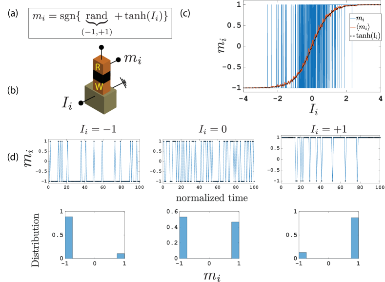
Any random signal generator whose randomness can be tuned with a third terminal should be a suitable building block for PSL. The icon in Fig. 1b represents our generic building block whose input controls the output according to the equation (Fig. 1a),
| (1) |
where rand(1,+1) represents a random number uniformly distributed between 1 and +1. It is assumed to change every seconds which represents the retention time of individual p-bits. We normalize the time axis to so that t is dimensionless and progresses in steps (0, 1, 2, ). At each time step, if the input is zero, the output takes on a value of 1 or +1 with equal probability, as shown in the middle panel of Fig. 1d. A negative input makes negative values more likely (left panel) while a positive input makes positive values more likely (right panel). Fig. 1c shows as the input is ramped from negative to positive values. Also shown is the time-averaged value of which equals .
A possible physical implementation of p-bits could use stochastic nanomagnets with low energy barriers whose retention time Lopez-Diaz et al. (2002):
is very small, on the order of which is a material dependent quantity called the attempt time and is experimentally found to be Lopez-Diaz et al. (2002) among different magnetic materials. Such stochastic nanomagnets can be pinned to a given direction with spin currents that are at least an order of magnitude less than those needed to switch 40 kT magnets. The sigmoidal tuning curve in Fig. 1c describing the time average of a fluctuating signal represents the essence of a p-bit. Purely CMOS implementations of a p-bit are possible Palem and Lingamneni (2013); Cheemalavagu et al. (2005), but the sigmoid seems like a natural feature of nanomagnets driven by spin currents. Indeed, the use of stochastic nanomagnets in the context of random number generators, stochastic oscillators and autonomous learning Fukushima et al. (2014); Choi et al. (2014); Grollier et al. (2016) has been discussed in the literature. But performing “invertible” Boolean logic utilizing large scale correlations has not been discussed before to our knowledge.
Note that we are using the term invertibility in the broader sense of relation inverses and not in the narrower sense of function inverses. For example, AND, when interpreted as a relation, consists of the set where each term is of the form . The relation inverse of 0 is the set even though the corresponding functional inverse is not defined. What our scheme provides, probabilistically, is the relation inverse inv ; Canetti and Varia (2009).
Ensemble-average versus time-average: A sigmoidal response was presented in Behin-Aein et al. (2016) for the ensemble-averaged magnetization of large barrier magnets biased along a neutral state. This was proposed as a building block for both Ising computers as well as directed belief networks and a recent paper Shim et al. (2017) describes a similar approach applied to a graph coloring problem. By contrast low barrier nanomagnets provide a sigmoidal response for the time-averaged magnetization and a suitably engineered network of such nanomagnets could cycle through the collective states at GHz rates, with an emphasis on the “low energy states” which can encode the solution to the combinatorial optimization problems, like the traveling salesman problem (TSP) as shown in Sutton et al. (2017). Once the time-varying magnetization has been converted into a time-varying voltage through a READ circuit, a simple RC circuit can be used to extract the answer through a moving time average. For example, in Fig. 1c the red trace was obtained from the rapidly varying blue trace using an RC circuit in a SPICE simulation.
The central feature underlying both implementations is the p-bit that acts like a tunable random number generator, providing an intrinsic sigmoidal response for the ensemble-averaged or the time-averaged magnetization as a function of the spin current. It is this response that allows us to correlate the fluctuations of different p-bits in a useful manner by interconnecting them according to
| (2) |
where provides a local bias to magnet and defines the effect of bit j to bit i, and sets a global scale for the strength of the interactions like an inverse “pseudo-temperature” giving a dimensionless current to each p-bit. The computation of in terms of in Eq. (2) is assumed instantaneous, in hardware implementations there can be interconnect delays that relate to currents at a later time, .
Equation (1) arises naturally from the physics of low barrier nanomagnets as we have discussed above. Equation (2) represents the “weight logic” for which there are many candidates such as memristors Yang et al. (2013), floating-gate based devices Diep et al. (2014), domain-wall based devices Sengupta et al. (2016), standard CMOS Yamaoka et al. (2016). The suitability of these options will depend on the range of J values and the sparsity of the J-matrix.
Equations (1-2) are essentially the same as the defining equations for Boltzmann machines introduced by Hinton and his collaborators Ackley et al. (1985) which have had enormous impact in the field of machine learning, but they are usually implemented in software that is run on standard CMOS hardware. The primary contributions of this paper are threefold:
-
•
Hardware implementation: It may seem “obvious” that an unstable magnet could provide a natural hardware for representing a p-bit, but we would like to stress a less obvious point. To the best of our knowledge, simple two-terminal devices are not suitable for constructing large scale correlated networks of the type envisioned here. Instead, we need three-terminal building blocks with transistor-like gain and input-output isolation as shown in Fig. 1b Behin-Aein et al. (2016). To stress this point, we describe a concrete implementation of a Boolean function using detailed nanomagnet and transport simulations that are in good agreement with those obtained by the generic model based on Eq. (1). All other results in this paper are based on Eq. (1) in order to emphasize the generality of the concept of p-bits which need not necessarily be nanomagnet-based Yamaoka et al. (2015); Inagaki et al. (2016).
-
•
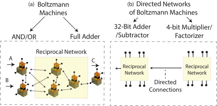
Boltzmann machines (BM) for invertible Boolean logic (Fig.2a): Much of the current emphasis on BMs is on “learning” giving rise to the concept of restricted Boltzmann machines Salakhutdinov et al. (2007). By contrast this paper is about Boolean logic, extending an established method for Hopfield networks Amit (1992) to provide a mathematical prescription to turn any Boolean truth table into a symmetric J-matrix (Eq. (2), with ), in one shot with no “learning” being involved. This design principle seems quite robust, functioning satisfactorily even when the J-matrix elements are rounded off, so that the required interconnections are relatively sparse and quantized which simplifies the hardware implementation. The numerical probabilities agree well with those predicted from the energy functional.
(3) using the Boltzmann law:
(4) Most importantly we show that the resulting Boolean gates are invertible: not only do they provide the correct output for a given input, for a given output they provide the correct input(s). If the given output is consistent with multiple inputs, the system fluctuates among all possible answers. This remarkable property of invertibility is absent in standard digital circuits and could help provide solutions to the Boolean satisfiability problem (Fig. 8) Du et al. (1997).
-
•
Directed networks of BM (Fig.2b): Finally we show that individual BM’s can be connected to perform precise arithmetic operations which are the norm in standard digital logic, but quite surprising for BM which are more like a collection of interacting particles than like a digital circuit. We show that a 32-bit adder converges to the one correct sum out of billion possibilities when the interaction parameter is suddenly turned up from say to . This can be likened to quenching a molten liquid and getting a perfect crystal. What we expect is plenty of defects, distributed differently everytime we do the experiment. That is exactly what we get if the individual BM Full adders comprising the 32-bit adder are connected bidirectionally (). But by making the connection between Adders directed (), we obtain the striking accuracy of digital circuits while largely retaining the invertibility of BM. This is a key result that we establish with extensive examples including a 4-multiplier which in inverted mode functions as a factorizer.
Each of these three contributions is described in detail in the three sections that follow.
II An example hardware Implementation of PSL
To ensure that individual p-bits can be interconnected to produce robust correlations, it is important to have separate terminals for writing (more correctly biasing) and reading, marked W and R respectively in Fig. 3a. With IMA nanomagnets (e.g circular nanomagnets) this could be accomplished following existing experiments Liu et al. (2012); Locatelli et al. (2014) using the giant spin Hall effect (GSHE). Recent experiments using a built-in exchange bias van den Brink et al. (2016); Lau et al. (2016); Smith et al. (2016); Fukami et al. (2016) could make this approach applicable to PMA as well. Note however, that these experiments have all been performed with stable free layers, and would have to be carried out with low barrier magnets in order to establish their suitability for the implementation of p-bits. As the field progresses, one can expect the bias terminal to involve voltage control Heron et al. (2014); Manipatruni et al. (2015) instead of current control, just as the output could involve quantities other than magnetization. We will now show a concrete implementation of a Boolean function using minimal CMOS circuitry in conjunction with stochastic nanomagnets through detailed nanomagnet and transport simulations that are in good agreement with those obtained from the generic model based on Eq. (1).
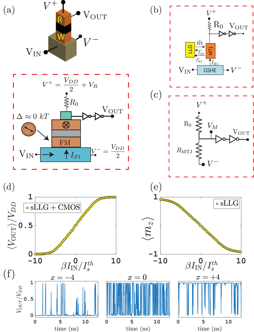
Fig. 3a shows a possible, CMOS-assisted p-bit that has a separate READ and WRITE path. The device consists of a heavy metal exhibiting Giant Spin Hall Effect (GSHE) that drives a circular magnet which replaces the usual elliptical magnets in order to provide the stochasticity needed for the magnetization. A small read current, which is assumed to not disturb the magnetization of the free layer in our design, that flows through the fixed layer is used to sense the instantaneous magnetization, which is amplified and isolated by two inverters that act as a buffer. This structure is very similar to the experimentally demonstrated GSHE switching of elliptical magnets that were similarly read-out by an MTJ Liu et al. (2012), with the only exception that the elliptical magnets are replaced by circular magnets with an aspect ratio of one. This device could be viewed as replacing the free layers of the GSHE-driven MTJs demonstrated in Liu et al. (2012) with those in the telegraphic regime Koch et al. (2000); Urazhdin et al. (2003); Krivorotov et al. (2004); Locatelli et al. (2014) .
In the presence of thermal noise the magnetization of such a circular magnet rotates in the plane of the circle without a preferred easy-axis that that would have arisen due to the shape anisotropy, effectively making its thermal stability Khvalkovskiy et al. (2013). This magnetization can be pinned by a spin current that is generated by flowing a charge current through the GSHE layer. The magnetic field driven sigmoidal responses of magnetization for such circular magnets have experimentally been demonstrated Cowburn (2000); Debashis et al. (2016), while the spin current driven pinning has not been demonstrated to our knowledge. Using validated modules for transport and magnetization dynamics Camsari et al. (2015) (Fig. 3b), we solve the stochastic Landau-Lifshitz-Gilbert (sLLG) equation in the presence of thermal noise and a GSHE current. The following subsection shows detailed simulation parameters.
Sigmoidal response: A long-time average ( of the magnetization as a function of a GSHE-generated spin current is plotted in Fig. 3e that displays the desired sigmoidal characteristic for p-bits dictated by Eq. (1). The x-axis of Fig. 3e is normalized to the geometric gain factor that relates the charge current to the spin current exerted Liu et al. (2011); Hong et al. (2016):
| (5) |
where is the Hall angle, is the thickness and is the spin-relaxation length of the heavy metal. The quantity can be made to be much greater than 1 providing an intrinsic gain Datta et al. (2012a), however for the parameters used in the present examples, is .
Another quantity that is used to normalize the x-axis of Fig. 3e is the “thermal spin current” that corresponds to the strength of the thermal noise that needs to be overcome for a circular magnet to be pinned in a given direction:
| (6) |
where q is electron charge, is the damping coefficient of the magnet. , and all have units of charge current, therefore we can define the dimensionless interaction parameter, of Eq. 2 as .
It can be seen from Fig. 3e that when the applied spin current , the magnetization of the circular magnet is pinned in the directions for these particular parameters. For PMA magnets with low barriers (), the pinning current is independent of the volume as long as increasing the volume does not invalidate the assumption. This can be analytically shown from a 1D Fokker-Planck equation Butler et al. (2012), and we have reproduced this behavior directly from sLLG simulations. For the in-plane (circular) magnets considered here, the pinning current in general has a and dependence and the dimensionless pinning current can be larger.
Nevertheless, it is possible to estimate the thermal spin current for typical damping coefficients of , is . Pinning currents for superparamagnets are at least an order of magnitude smaller than the critical switching currents of stable magnets Kent and Worledge (2015). , defined by Eq. (6) also sets the scale for defined in Eq. (2) suggesting that a stochastic nanomagnet based implementation of PSL could be more energy efficient than the standard spin-torque switching of stable magnets that suffer from high current densities.
Need for three-terminal devices with READ-WRITE separation: Note that a crucial function of the READ circuit and the CMOS transistors in this design is the ability to turn the magnetization into an output voltage that is proportional to , providing gain for fan-out and isolation to avoid any read disturb. Indeed, a critical requirement for any other alternative implementations of p-bits is the need for three terminal devices with separate READ and WRITE paths to provide gain and isolation. In this particular design these features come in by directly integrating CMOS transistors, but CMOS-free, all-magnetic designs with these characteristics have been proposed Datta et al. (2012a); Morris et al. (2012). Our purpose is to simply show how a p-bit can be realized by using experimentally demonstrated technology. Alternative designs are beyond the scope of this paper.
READ Circuit: For the output to provide symmetric voltage swings on the GSHE layer, the minus supply needs to be set to since ranges between 0 and . is set to where is a small READ voltage that is amplified by the inverters. We assume a simple, bias-independent MTJ model Datta et al. (2012b):
| (7) |
where P is the interface polarization and is the average MTJ conductance. Setting the reference resistance (Fig. (3c)) equal to , the input voltage to the inverters, in FIG. (2d) becomes:
| (8) |
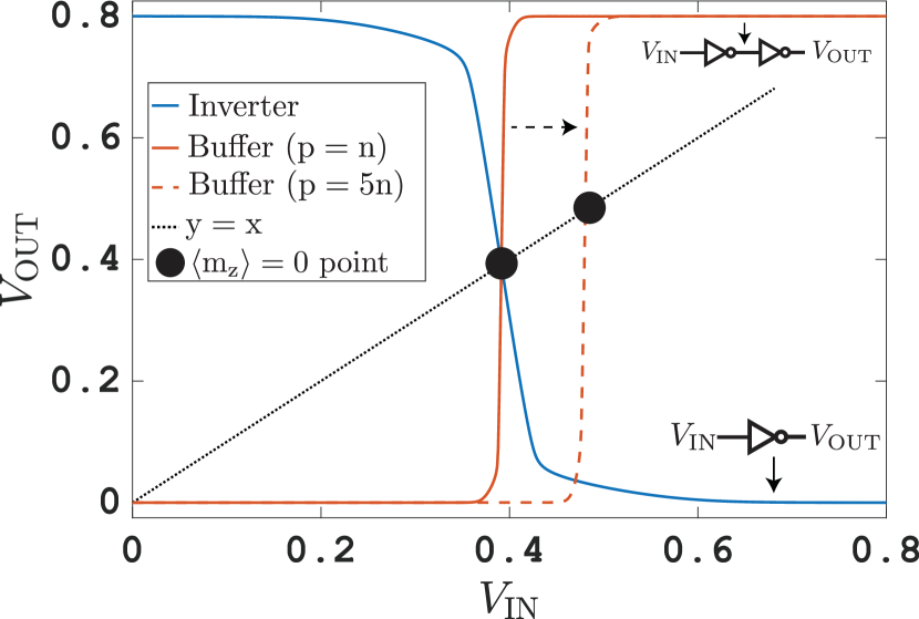
In the absence of a bias becomes and the middle voltage fluctuates around the mean . This requires the inverter characteristic to be shifted to this value to produce a telegraphic output that fluctuates between 0 and with equal probability (Fig. 3f). This shift is easily engineered by sizing the pFET and nFET transistors differently, a wider pFET shifts the inverter characteristic towards , as we will show in the next subsection.
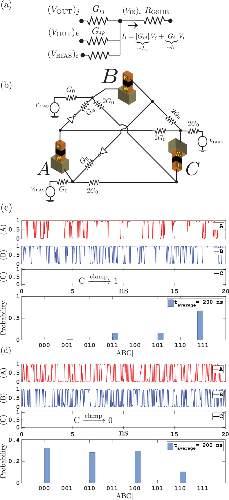
Interconnection matrix: A passive resistor network can be used as a possible interconnection scheme to correlate the p-bits as shown in Fig. 4. A proper design of the interconnection matrix J that has only a few discrete values ensures a minimal number of different conductances (). In this demonstrated example the AND gate requires only 2 unique, discrete conductance values.
The spin currents that need to be delivered to each p-bit are on the order of a few and can be generated with charge currents that are even smaller, due to the GSHE gain. This means the interconnection resistances could be on the order of 100 k’s since the voltage drops across these resistances are around V. Since the GSHE ground simply shifts all the voltages to get symmetric swings, we define the voltages . Then input currents to each p-bit can be expressed (Fig. 4a):
| (9) |
assuming since the heavy metal resistances are typically much less than hundreds of k. We have verified the validity of Eq. (9) by SPICE simulations, for the parameters chosen for these examples.
As a result, we observe that Eq. (9) constitutes a hardware mapping for the interconnections of Eq. (2). In this scheme conductances are initially adjusted to obtain a global interaction strength for a given problem. Alternatively, the interaction strength can be adjusted electrically by varying the supply voltages.
Invertible AND Gate: Fig. 4b shows an explicit implementation of an invertible AND gate ( corresponding to [J] and matrices Biamonte (2008) that have 3 unique, integer entries:
| (10) |
In Fig. 4d, we show the inverse operation of the AND gate where we clamp the output bit C to a 0 or 1 by the bias voltage attached to its input terminal. The interconnection resistance is chosen to be that roughly provides A of charge current to each p-bit, corresponding to an for the chosen parameters.
Generating the histogram: At the end of the simulation (t=200 ns), we threshold the voltage output of A,B and C by legislating all voltages above to be 1, and below to be 0. Then a histogram output for the thresholded word [ABC] is obtained and normalized to unit probability. Clamping the output to 0 and letting A and B float, make A and B fluctuate in a correlated manner and they visit the three possible states (00, 01, 10) with approximately equal probability. Resolving the output 0 to the three possible input combinations is, in a way “factorizing” the output. Conversely, clamping the output to 1 produces a strong (11) peak in the histogram of [ABC], which is the only consistent input combination for C=1 (Fig. 4c-d).
Assumptions of the model: We have made several simplifying assumptions while modeling the hardware implementation of a p-bit. (1) The READ voltage that is amplified by the inverters produces a small current that passes through the circular magnet and might potentially disturb its current state. We assumed that this current (labeled as in Fig. 3b) is negligible and do not affect the magnetization of the stochastic magnet. (2) We assumed that the spin current generated by the heavy metal is deposited to the free layer with perfect efficiency ( in Fig. 3b), however, depending on the interface properties this conversion factor can be less than 100. (3) We have also assumed that the fixed layer does not produce a notable stray field on the circular magnet. Note that the presence of such a constant field would simply shift the sigmoidal behavior presented in Fig. 3d-e to the right (or left) and could have been offset by a constant bias current. (4) Finally, we have neglected the resistance of the GSHE portion in the READ circuit (Fig. 3c), assuming the MTJ resistance would be dominant in this path.
Detailed Simulation Parameters
This section shows the details of simulation parameters for the hardware implementation of p-bits that are used for Fig. 34.
sLLG for stochastic circular magnets: The magnetization of a circular nanomagnet described as is obtained from the stochastic Landau-Lifshitz-Gilbert (sLLG) equation:
| (11a) | |||
where is the damping coefficient, q is the electron charge, is the electron gyromagnetic ratio, is the spin current that is assumed to be uniformly distributed over the total number of spins in the macrospin, , being the Bohr magneton. It is assumed that the spin current generated from the GSHE layer is polarized in the z-direction, such that . is the effective field of the circular magnet, where the uniaxial anisotropy is assumed to be negligible, but there is still a strong demagnetizing field. The thermal fluctuations also enter through the effective magnetic field: , -axis being the out-of-plane direction of the magnet, and in units [] with zero mean, and equal in all three directions. Table 1 shows the parameters used in Figs. 34. We note that this parameter selection is simply one possibility, many other parameters could have been used with no change in the basic conclusions.
| Parameters | Value |
|---|---|
| Saturation magnetization () | 300 emu/cc |
| Magnet diameter (), thickness (t) | 15 nm, 0.5 nm |
| MTJ Polarization (P) (Eq. (7)) | 0.5 |
| MTJ Conductance () (Eq. (7)) | 176 S |
| Damping coefficient () | 0.1 |
| Spin Hall Length, Width (Eq. (5)) | nm |
| Hall Angle, Spin relax. length | =0.5 Demasius et al. (2016), 2.1 nmPai et al. (2012) |
| Spin Hall res. , thickness () | 200 -cm Hao and Xiao (2015), 3.15 nm |
| Temperature () | 300 K |
| CMOS Models | 14nm HP-FinFET pre |
| Supply and READ Voltage | , |
| Timestep for transient sim. (SPICE) | t = 0.05 ps |
Obtaining the sigmoidal response of CMOS+sLLG: Each data point in the sigmoids shown in Figs. 34 is obtained by averaging the z-component of the magnetization after 500 ns, with a time-step of . The CMOS inverter characterestics in conjunction with a spherical representation-based sLLG are obtained using the modular framework developed in Camsari et al. (2015) using HSPICE.
14 nm FinFET Inverter Characteristics: Fig. 5 shows the input/output characteristics of the single and double inverters that are used to amplify the stochastic signal that is generated by the MTJ (Fig. 3). At zero-bias from the GSHE, the amplified signal (Eq. 8) is in the middle of and which is . The buffer response can be shifted to this value by increasing the size of pFETs, as shown in Fig. 5.
III Invertible Boolean logic with Boltzmann Machines
We now present a mathematical prescription that shows how any given truth table can be implemented in terms of Boltzmann Machines, in “one shot” with no learning being involved, unlike much of the past work in this area (See for example, Sejnowski et al. (1986); Patarnello and Carnevali (1987)). In Section II, we chose a simple [J] and matrix to implement an AND gate based on Biamonte (2008). In this section, we outline a general approach to show how any truth table can be implemented in terms of such matrices. Our approach, pictorially described in Fig. 6, begins by transforming a given truth table from binary to bipolar variables. The lines of the truth table are then required to be eigenvectors each with eigenvalue +1, all other eigenvectors are assumed to have eigenvalues equal to 0. This leads to the following prescription for J as shown in Fig. 6:
| (12a) | |||
| (12b) | |||
where are the eigenvectors corresponding to lines in the truth table of a Boolean operation and S is a projection matrix that accounts for the non-orthogonality of the vectors defined by different lines of the truth table. Note that the resultant J-matrix is always symmetric () with diagonal terms that are subtracted in our models such that . The number of p-bits in the system is made greater than the number of lines in a truth table through the addition of hidden units (Fig. 6) to ensure that the number of conditions we impose is less than the dimension of the space defined by the number of p-bits.
Another important aspect in the construction of [J] is that an eigenvector implies that its complement is also a valid eigenvector. However only one of these might belong to a truth table. We introduce a “handle” bit to each that is biased to distinguish complementary eigenvectors. These handle bits provide the added benefit of reconfigurability. For example, AND and OR gates have complementary truth tables, and a given gate can be electrically reconfigured as an AND or an OR gate using the handle bit.
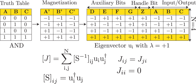
J-Matrices for AND/FA: We now provide the details of the J-matrix for the AND gate, obtained using the prescription shown in Fig. 6 based on Eq. (12a). The eigenvectors of the truth table for the AND in Fig. 6 are placed into a matrix U, such that , where is the first row of the matrix shown in Fig. 6, and so on. In matrix notation, the S-matrix can be written as:
| (13) |
Then the J-matrix becomes:
| (14) |
Removing the diagonal entries by making and multiplying the matrix entries by 2, to obtain simple integers, evaluates to:
| (15) |
with the notation, [1-5: auxiliary bit and handle bit, 6:“A”, 7:“B”, 8:“C”]. Following a similar procedure, we use the following Full Adder matrix, :
| (16) |
with the notation, [19: auxiliary bits and handle bit, 10: “”, 11: “B”, 12: “A”, 13: “S” 14: “”].
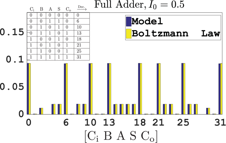
These are the J-matrices (AND and FA) that are used for all examples in the paper, except for the AND gate described in Section II. Fig. 10 shows the “truth table” operation of the Full Adder where all input/output terminals are “floating” using the J-matrix of Eq. (16), showing excellent quantitative agreement with the Boltzmann distribution of Eq. (4) at steady state even for the undesired peaks of the truth table.
Note that this prescription for [J] is similar to the principles developed originally for Hopfield networks (Personnaz et al. (1986), and Eq. (4.20) in Amit (1992)). However, other approaches are possible along the lines described in the context of Ising Hamiltonians for quantum computers Biamonte (2008). We have tried some of these other designs for [J] and many of them lead to results similar to those presented here. For practical implementations, it will be important to evaluate different approaches in terms of their demands on the dynamic range and accuracy of the weight logic.
Description of universal model: Once a J-matrix and the h-vector are obtained for a given problem, the system is initialized by randomizing all at time, . First, the current (voltage) that a given p-bit () feels due to the other coupled is obtained from Eq. (2), and the value is updated according to Eq. (1). Next the procedure is repeated for the remaining p-bits by finding the current they receive due to all other using the updated values of . For this reason, the order of updating was chosen randomly in our models and we found that the order of updating has no effect in our results. However, updating the p-bits in parallel leads to incorrect results. These two observations are well-known in the context of Hopfield networks and Boltzmann Machines Aiyer et al. (1990); Suzuki et al. (2013); Hinton (2007). This type of serial updating corresponds to the “asynchronous dynamics” Hopfield (1982); Amit (1992). We note that the hardware implementation discussed in this paper naturally leads to an asynchronous updating of p-bits in the absence of a global clock signal. We have set up an online simulator based on this model in Ref. Sutton et al. (2017b) so that interested readers can simulate some of the examples discussed in this paper.
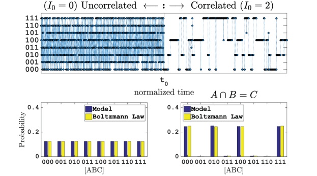
Fig. 7 shows the time evolution of an AND based on Eq. (15). Initially for the interaction strength is zero (), making the pseudo-temperature of the system infinite and the network produces uncorrelated noise visiting each state with equal probability. In the second phase (), the interaction strength is suddenly increased to , effectively “quenching” the network by reducing the temperature. This correlates the system such that only the states corresponding to the truth table of the AND gate are visited, each with equal probability when a long time average is taken. The average probabilities in each phase quantitatively match the Boltzmann Law defined by Eq. (4).
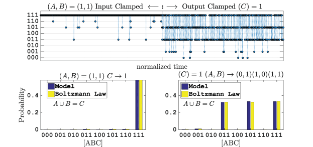
In Fig. 8, we show how a correlated network producing a given truth table can be used to do directed computation analogous to standard CMOS logic. An OR gate is constructed by using the same [J] matrix for an AND gate, but with a negated handle bit. By “clamping” the input bits of an OR gate () through their bias terminals, , to (A,B)=(+1,+1), the system is forced to only one of the peaks of the truth table, effectively making C=1.
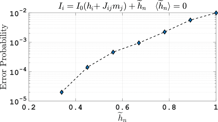
The PSL gates however exhibit a remarkable difference with standard logic gates, in that inputs and outputs are on an equal footing. Not only do clamped inputs give the corresponding output, a clamped output gives the corresponding input(s). In the second phase () the output of the OR gate is clamped to +1, that produces three possible peaks for the input terminals, corresponding to various possible input combinations that are consistent with the clamped output (A,B)=(0,1),(1,0) and (1,1). The probabilistic nature of PSL allows it to obtain multiple solutions (Fig. 8c). It also seems to make the results more resilient to unwanted noise due to stray fields that are inevitable in physical implementations as shown in Fig. 9. Here, we simulate an AND gate in the presence of a normally distributed random noise that enters the bias fields of each p-bit and define the computation to be faulty, if the mode (most frequent value) of the output bit is not consistent with the programmed input combinations after time steps. We observe that even large levels of uncontrolled noise produces correct results with high probabilities.
Fig. 10 shows the design of a Full Adder (FA) with the 8-line truth table shown. There are three inputs in all, two from the numbers to be added, and one carry bit from previous FA. It produces two outputs, one the sum bit and the other a carry bit to be passed on to the next FA. The probabilities of different states are calculated using from Eq. (16), with in the truth table mode, where all inputs and outputs are floating and the states are numbered using the decimal number corresponding to the binary word . The decimal numbers corresponding to the truth table are shown in the inset, and these match the location of the taller peaks in the histogram. Note that the Boltzmann distribution (Eq. (4)) quantitatively matches the model even for the suppressed peaks. A higher reduces these suppressed peaks further. The statistics are collected for steps, and each terminal output is then placed in the histogram.
IV Directed Networks of Boltzmann Machines
When constructing larger circuits composed of individual Boltzmann machines, the reciprocal nature of the Boltzmann machine often interferes with the directed nature of computation that is desired. It seems advisable to use a hybrid approach. For example in constructing a 32-bit adder we use Full-Adders (FA) that are individually BMs with symmetric connections, . But when connecting the carry bit from one FA to the next, the coupling element is non-zero in only one direction from the least significant to the most significant bit. This directed coupling between the components distinguishes PSL from purely reciprocal Boltzmann machines. Indeed, even the Full Adder could be implemented not as a Boltzmann machine but as a directed network of more basic gates. But then it would lose its invertibility. On the other hand, the directed connection of BM Full Adders largely preserves the invertibility of the overall system as we will show.
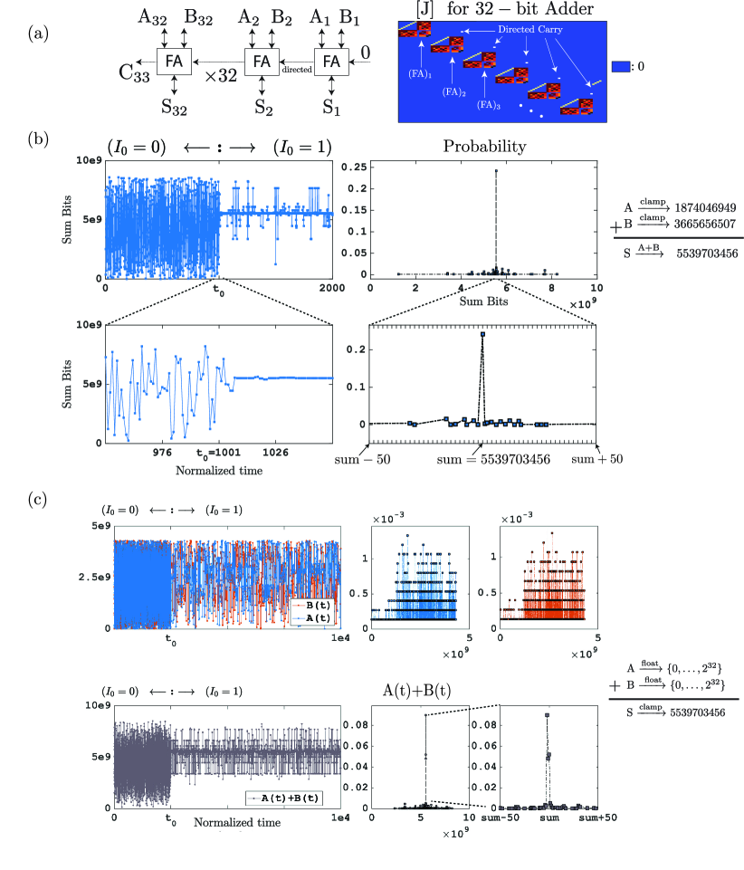
32-bit Adder/Subtractor
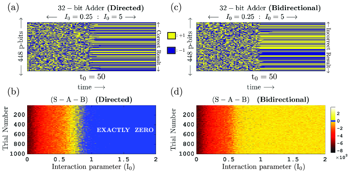
Fig. 11 shows the operation of a 32-bit adder that sums two 32-bit numbers A and B to calculate the 33-bit sum S. In the initial phase () we have corresponding to infinite temperature so that the sum bits (S) fluctuate among 8 billion possibilities. With = 1, Fig. 11 shows that the correct answer has a probability of which is much lower than the that can be achieved with larger values (as in Fig.13 a-c with =5). Nevertheless the peak is unmistakable as evident from the expanded scale histogram and the correct answer is extracted from the majority vote of =100 samples as shown in Fig. 13. This ability to extract the correct answer despite large fluctuations is a general property of probabilistic algorithms.
Interestingly, although the overall system includes several unidirectional connections, it seems to be able to perform the inverse function as well. With A and B clamped it calculates S=A+B as noted above. Conversely with S clamped, the input bits A and B fluctuate in a correlated manner so as to make their sum sharply peaked around S. Fig. 11 shows the time evolution of the input bits that have broad distributions spanning a wide range. Initially, when is small, the sum of A and B also shows a broad distribution, but once is turned up to 1, the distributions of A and B get strongly correlated making the distribution of A+B sharply peaked around the fixed value of S. It must be noted that the 32-bit adder shown in Fig. 11 is not like standard digital circuits which are not invertible. The demonstration of such an invertible 32-bit adder could be practically significant, since binary addition is noted to be the most fundamental and frequently used operation in digital computing Liu et al. (2003).
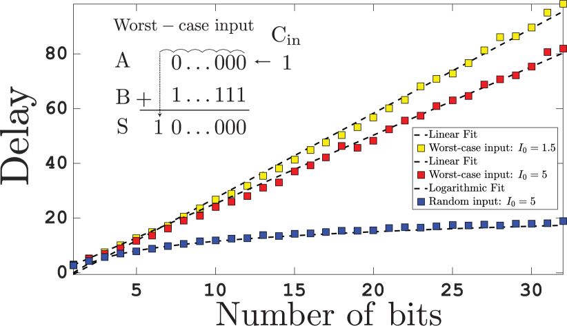
Delay of Ripple Carry Adder: Just as in CMOS-based Ripple Carry Adders, the delay of the p-bit based RCA is a function of the inputs A and B. In Fig. 12 we have systematically studied the worst-case delay of the p-bit based Ripple Carry Adder (RCA) as a function of increasing bit size. We selected a “worst-case” combination that results in a carry that needs to be propagated from bit 1 to bit N which results in a linear increase in the delay, exhibiting O(n) complexity with input size similar to CMOS implementations Uma et al. (2012). When the inputs are random, the delay seems to increase sub-linearly. The system is quenched at t=0 for different interaction parameters and the delay is defined to be the time it takes for the system to settle to the mode of the array for =200. An error check has been carried out separately to ensure the calculated sum (mode) is always exactly equal to the expected sum. For random inputs the 32-bit adder is close to 20 time steps, in accordance with the example shown in Fig. 11.
Digital accuracy AND logical invertibility: The striking combination of accuracy and invertibility is made possible by our hybrid design, whereby the individual Full Adders are Boltzmann Machines, even though their connection is directed. Our 32-bit adder is more like a collection of interacting particles than like a digital circuit as evident from Fig. 13a which shows a colormap of the binary state of each of the 448 p-bits as a function of time with the interaction parameter suddenly increased from 0.25 to 5 at , thereby quenching a “molten liquid” into a “solid”. Nevertheless it shows the striking accuracy of a digital circuit, with SAB exactly equal to zero in each of the 1000 trials as shown in Fig. 13b. We do not expect a “molten liquid” to be quenched into a “perfect crystal” every time. Instead, we would expect a “solid full of defects” with different non-zero values for SAB in each trial. That is exactly what we get if the carry bits are bidirectional as in a fully BM implementation (Fig. 13d).
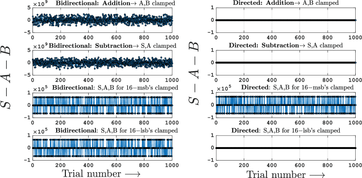
Note however, that this digital accuracy is achieved while maintaining the property of invertibility that is absent in digital circuits. Fig. 13 is not for direct mode operation, but for the adder operating in reverse mode as a subtractor. It might be expected that the directed connection of carry bits from the less significant to the more significant bit could lead to a loss of invertibility. To investigate this point, we show the error SAB as a function of trial number (Fig. 14) for four different modes of operation with (i) A and B clamped (Addition), (ii) S and A clamped (Subtraction), (iii) A, B and S for the 16 most significant bits (msb) clamped, and (iv) A, B and S for the 16 least significant bits (lsb) clamped. The fully bidirectional implementation shows very large errors for all modes of operation. The directed implementation, on the other hand, works perfectly for both the adder and the subtractor modes. It also works if we clamp the least significant bits, but not if we clamp the most significant bits. This seems reasonable since we expect to be able to control a flow by making changes upstream (lsb), but not downstream (msb).
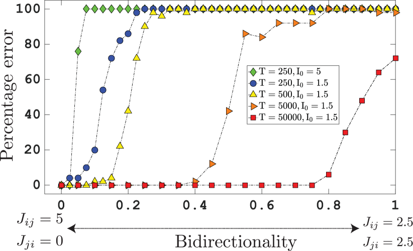
Partial directivity: So far in our examples we have only considered fully directed () or fully bidirectional () carry bits when connecting the individual Full Adders. In Fig. 15 we systematically analyze the effects of partial directivity in the operation of a 32-bit adder. We observe that the 32-bit adder operates correctly even when there is large degree of bidirectionality () provided that the system is allowed to run for a long time, , in stark contrast with the fully directed case that could resolve the right answer within , shown in Fig. 14b. Decreasing the time steps systematically increases the error. Increasing the correlation parameter while keeping constant also seems to adversely affect the bidirectional designs, that might be getting the system stuck in local minima.
Directionality and computation time, 2 p-bit model: The qualitative relation between , and bidirectionality described above is derived from extensive numerical simulations based on Eq. 1-2. However, the broad features can be understood from a model involving just two p-bits, 1 and 2, with
It is straightforward to write a master equation describing the time evolution of the probabilities of different configurations:
being the transition matrix Amit (1992), representing the probability of both p-bits being , both being , and so on. We can write two matrices and describing the updating of p-bits 1 and 2 respectively:
where represents the probability that state makes a transition to state , and , . and are obtained from Eq. 1-2:
The overall transition matrix is given by or depending on which bit is updated first. Either way the matrix has four eigenvalues and and the corresponding eigenvectors evolve with time .
The components corresponding to =0 decay instantaneously while the eigenvector corresponding to =1 is the stationary result representing the correct solution. But for the system to reach this state, we have to wait for the fourth eigenvector corresponding to to decay sufficiently. A fully directed network has =0, so that and the system quickly reaches the correct solution. But in a bidirectional network with , the fourth eigenvalue can be quite close to one, especially for large and take an exponentially long time to decay, as when is close to 1.
This 2 p-bit model provides some insight into our general observation that directivity can be used to obtain accurate answers quickly. However, depending on the problem at hand it may be desirable to retain some degree of bidirectionality, since full directivity does lead to some loss of invertibility as seen for one set of inputs in Fig. 14. An example of a partially directed p-bit network is discussed in the next section.
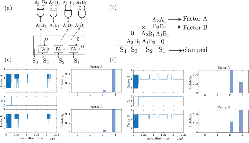
4-Bit Multiplier / Factorizer
Fig. 16 shows how the invertibility of PSL logic blocks can be used to perform integer factorization using a multiplier in reverse. Normally, the factorization problem requires specific algorithms Knuth and Pardo (1976) to be performed in CMOS-like hardware, here we simply use a digital 4-bit multiplier working in reverse to achieve this operation.
Specifically with the output of the multiplier clamped to a given integer from 0 to 15, the input bits float to the correct factors. The interconnection strength is increased suddenly from 0 to 2 at (Fig. 16) and the input bits get locked to one of the possible solutions. For example, when the output is set to 9, both inputs float to 3. With the output set to 6, both inputs fluctuate between two values, 2 and 3. Note that factors like do not show up, since encoding 9 in binary requires 4-bits (1001) and the input terminals only have 2-bits. We have checked other cases where factorizing 3 shows both and , and factorizing zero shows all possible peaks since there are many solutions such that and so on.
We also kept the same directed connections between the Full Adders for the carry bits, making them a directed network of Boltzmann Machines, similar to the 32-bit Adder. Moreover, we kept a directed connection from the Full Adders to the AND gates as shown in Fig. 16a since the information needs to flow from the output to the input in the case of factorization. The input bits that go to multiple AND gates are “tied” to each other with a positive exchange () value much like 2-spins interacting ferromagnetically, however in PSL we envision these interactions to be controlled purely electrically. In this example, we have observed that the system is sensitive to the relative strengths of couplings within the AND gates and between the AND gates and the Full Adders which can also depend on a chosen annealing profile.
The design of factorizers of practical relevance is beyond the scope of this paper. Our main purpose has been to establish how the key feature of invertibility of p-bits can be creatively used for different circuits with unique functionalities. The demonstration of 4-bit factorization through reverse multiplication is similar to memcomputing Traversa and Ventra (2017) based on deterministic memristors. Note, however, that the building blocks and operating principles of stochastic p-bits and memcomputing Di Ventra et al. (2016) are very different and the only similarity noted here is the fact that both approaches treat the input and output terminals on an equal footing.
V Summary
It is generally believed that (1) probabilistic algorithms can tackle specific problems much more efficiently than classical algorithms Ekert and Jozsa (1996), and that (2) probabilistic algorithms can run far more efficiently on a probabilistic computer than on a deterministic computer Feynman (1982); Ekert and Jozsa (1996). As such, it seems reasonable to expect that probabilistic computers based on robust room temperature p-bits could provide a practically useful solution to many challenging problems by rapidly sampling the phase space in hardware.
In this paper we have presented a framework for using probabilistic units or “p-bits” as a building block for a probabilistic spin logic (PSL) which is used to implement precise Boolean logic with an accuracy comparable to standard digital circuits, while exhibiting the unique property of invertibility that is unknown in deterministic circuits. Specifically we have:
-
•
presented an implementation based on stochastic nanomagnets to illustrate the importance of three-terminal building blocks in the construction of large scale correlated networks of p-bits. We emphasize that this is just one possible implementation that is by no means the only one (Section II).
-
•
presented an algorithm for implementing Boolean gates as BM with relatively sparse and quantized J-matrix elements, benchmarked their operation against the Boltzmann law, and established their capability to perform not just direct functions but also their inverse (Section III), and
-
•
presented a 32-bit adder implemented as a hybrid BM that achieves digital accuracy over a broad combination of the interaction parameter , directionality and the number of samples . This striking accuracy is reminiscent of digital circuits, but it is achieved while preserving a certain degree of invertibility which is absent in digital circuits. The accuracy is particularly surprising with high degrees of bidirectionality () where the system is picking out the one correct answer out of nearly 8 billion possibilities. This may require a larger number of time samples, but these could be collected rapidly at GHz rates. (Section IV).
We hope these findings will help emphasize a new direction for the field of spintronic and nanomagnetic logic by shifting the focus from stable high barrier magnets to stochastic, low barrier magnets, while inspiring a search for other possible physical implementations of p-bits.
Acknowledgements.
It is a pleasure to acknowledge many helpful discussions with Behtash Behin-Aein (Globalfoundries) and Ernesto E. Marinero (Purdue University). We thank Jaijeet Roychowdhury (UC Berkeley) for suggesting the phrase “invertible”. This work was supported in part by C-SPIN, one of six centers of STARnet, a Semiconductor Research Corporation program, sponsored by MARCO and DARPA, in part by the Nanoelectronics Research Initiative through the Institute for Nanoelectronics Discovery and Exploration (INDEX) Center, and in part by the National Science Foundation through the NCN-NEEDS program, contract 1227020-EEC.References
- Lopez-Diaz et al. (2002) L Lopez-Diaz, L Torres, and E Moro, “Transition from ferromagnetism to superparamagnetism on the nanosecond time scale,” Physical Review B 65, 224406 (2002).
- Palem and Lingamneni (2013) Krishna Palem and Avinash Lingamneni, “Ten years of building broken chips: the physics and engineering of inexact computing,” ACM Transactions on Embedded Computing Systems (TECS) 12, 87 (2013).
- Cheemalavagu et al. (2005) Suresh Cheemalavagu, Pinar Korkmaz, Krishna V Palem, Bilge ES Akgul, and Lakshmi N Chakrapani, “A probabilistic cmos switch and its realization by exploiting noise,” in IFIP International Conference on VLSI (2005) pp. 535–541.
- Fukushima et al. (2014) Akio Fukushima, Takayuki Seki, Kay Yakushiji, Hitoshi Kubota, Hiroshi Imamura, Shinji Yuasa, and Koji Ando, “Spin dice: A scalable truly random number generator based on spintronics,” Applied Physics Express 7, 083001 (2014).
- Choi et al. (2014) Won Ho Choi, Yang Lv, Jongyeon Kim, Abhishek Deshpande, Gyuseong Kang, Jian-Ping Wang, and Chris H Kim, “A magnetic tunnel junction based true random number generator with conditional perturb and real-time output probability tracking,” in Electron Devices Meeting (IEDM), 2014 IEEE International (IEEE, 2014) pp. 12–5.
- Grollier et al. (2016) Julie Grollier, Damien Querlioz, and Mark D Stiles, “Spintronic nanodevices for bioinspired computing,” Proceedings of the IEEE 104, 2024–2039 (2016).
- (7) J. Roychowdhury, private communication.
- Canetti and Varia (2009) For an example of the use of “invertible relations”, see Ran Canetti and Mayank Varia, “Non-malleable obfuscation,” in Theory of Cryptography Conference (Springer, 2009) pp. 73–90.
- Behin-Aein et al. (2016) Behtash Behin-Aein, Vinh Diep, and Supriyo Datta, “A building block for hardware belief networks,” Scientific Reports 6, 29893 (2016).
- Shim et al. (2017) Y. Shim, A. Jaiswal, and K. Roy, Journal of Applied Physics 121, 193902 (2017).
- Sutton et al. (2017) B. Sutton, K. Y. Camsari, B. Behin-Aein, and S. Datta, Scientific Reports 7 (2017).
- Yang et al. (2013) J Joshua Yang, Dmitri B Strukov, and Duncan R Stewart, “Memristive devices for computing,” Nature nanotechnology 8, 13–24 (2013).
- Diep et al. (2014) Vinh Quang Diep, Brian Sutton, Behtash Behin-Aein, and Supriyo Datta, “Spin switches for compact implementation of neuron and synapse,” Applied Physics Letters 104, 222405 (2014).
- Sengupta et al. (2016) Abhronil Sengupta, Yong Shim, and Kaushik Roy, “Proposal for an all-spin artificial neural network: Emulating neural and synaptic functionalities through domain wall motion in ferromagnets,” IEEE Transactions on Biomedical Circuits and Systems (2016).
- Yamaoka et al. (2016) Masanao Yamaoka, Chihiro Yoshimura, Masato Hayashi, Takuya Okuyama, Hidetaka Aoki, and Hiroyuki Mizuno, “Ising computer,” Hitachi Review 65, 157 (2016).
- Ackley et al. (1985) David H Ackley, Geoffrey E Hinton, and Terrence J Sejnowski, “A learning algorithm for boltzmann machines,” Cognitive science 9, 147–169 (1985).
- Yamaoka et al. (2015) Masanao Yamaoka, Chihiro Yoshimura, Masato Hayashi, Takuya Okuyama, Hidetaka Aoki, and Hiroyuki Mizuno, “24.3 20k-spin ising chip for combinational optimization problem with cmos annealing,” in 2015 IEEE International Solid-State Circuits Conference-(ISSCC) Digest of Technical Papers (IEEE, 2015) pp. 1–3.
- Inagaki et al. (2016) Takahiro Inagaki, Kensuke Inaba, Ryan Hamerly, Kyo Inoue, Yoshihisa Yamamoto, and Hiroki Takesue, “Large-scale ising spin network based on degenerate optical parametric oscillators,” Nature Photonics (2016).
- Salakhutdinov et al. (2007) Ruslan Salakhutdinov, Andriy Mnih, and Geoffrey Hinton, “Restricted boltzmann machines for collaborative filtering,” in Proceedings of the 24th international conference on Machine learning (ACM, 2007) pp. 791–798.
- Amit (1992) Daniel J Amit, Modeling brain function: The world of attractor neural networks (Cambridge University Press, 1992).
- Du et al. (1997) Dingzhu Du, Jun Gu, Panos M Pardalos, et al., Satisfiability problem: theory and applications: DIMACS Workshop, March 11-13, 1996, Vol. 35 (American Mathematical Soc., 1997).
- (22) “Predictive Technology Model (PTM) (http://ptm.asu.edu/)” .
- Sutton et al. (2017b) B. Sutton, K. Y. Camsari, R. Faria, and S. Datta, http://dx.doi.org/doi:10.4231/D3C24QP4B “Probabilistic spin logic simulator,” (2017b).
- Liu et al. (2012) Luqiao Liu, Chi-Feng Pai, Y Li, HW Tseng, DC Ralph, and RA Buhrman, “Spin-torque switching with the giant spin hall effect of tantalum,” Science 336, 555–558 (2012).
- Locatelli et al. (2014) Nicolas Locatelli, Alice Mizrahi, A Accioly, Rie Matsumoto, Akio Fukushima, Hitoshi Kubota, Shinji Yuasa, Vincent Cros, Luis Gustavo Pereira, Damien Querlioz, et al., “Noise-enhanced synchronization of stochastic magnetic oscillators,” Physical Review Applied 2, 034009 (2014).
- van den Brink et al. (2016) Arno van den Brink, Guus Vermijs, Aurélie Solignac, Jungwoo Koo, Jurgen T Kohlhepp, Henk JM Swagten, and Bert Koopmans, “Field-free magnetization reversal by spin-hall effect and exchange bias,” Nature communications 7 (2016).
- Lau et al. (2016) Yong-Chang Lau, Davide Betto, Karsten Rode, JMD Coey, and Plamen Stamenov, “Spin–orbit torque switching without an external field using interlayer exchange coupling,” Nature nanotechnology (2016).
- Smith et al. (2016) Angeline Klemm Smith, Mahdi Jamali, Zhengyang Zhao, and Jian-Ping Wang, “External field free spin hall effect device for perpendicular magnetization reversal using a composite structure with biasing layer,” arXiv preprint arXiv:1603.09624 (2016).
- Fukami et al. (2016) Shunsuke Fukami, Chaoliang Zhang, Samik DuttaGupta, Aleksandr Kurenkov, and Hideo Ohno, “Magnetization switching by spin-orbit torque in an antiferromagnet-ferromagnet bilayer system,” Nature materials (2016).
- Heron et al. (2014) JT Heron, JL Bosse, Q He, Y Gao, M Trassin, L Ye, JD Clarkson, C Wang, Jian Liu, S Salahuddin, et al., “Deterministic switching of ferromagnetism at room temperature using an electric field,” Nature 516, 370–373 (2014).
- Manipatruni et al. (2015) Sasikanth Manipatruni, Dmitri E Nikonov, and Ian A Young, “Spin-orbit logic with magnetoelectric nodes: A scalable charge mediated nonvolatile spintronic logic,” arXiv preprint arXiv:1512.05428 (2015).
- Koch et al. (2000) Roger H Koch, G Grinstein, GA Keefe, Yu Lu, PL Trouilloud, WJ Gallagher, and SSP Parkin, “Thermally assisted magnetization reversal in submicron-sized magnetic thin films,” Physical review letters 84, 5419 (2000).
- Urazhdin et al. (2003) Sergei Urazhdin, Norman O Birge, WP Pratt Jr, and J Bass, “Current-driven magnetic excitations in permalloy-based multilayer nanopillars,” Physical review letters 91, 146803 (2003).
- Krivorotov et al. (2004) IN Krivorotov, NC Emley, AGF Garcia, JC Sankey, SI Kiselev, DC Ralph, and RA Buhrman, “Temperature dependence of spin-transfer-induced switching of nanomagnets,” Physical review letters 93, 166603 (2004).
- Khvalkovskiy et al. (2013) AV Khvalkovskiy, D Apalkov, S Watts, R Chepulskii, RS Beach, A Ong, X Tang, A Driskill-Smith, WH Butler, PB Visscher, et al., “Basic principles of stt-mram cell operation in memory arrays,” Journal of Physics D: Applied Physics 46, 074001 (2013).
- Cowburn (2000) RP Cowburn, “Property variation with shape in magnetic nanoelements,” Journal of Physics D: Applied Physics 33, R1 (2000).
- Debashis et al. (2016) Punyashloka Debashis, Rafatul Faria, Kerem Y Camsari, Joerg Appenzeller, Supriyo Datta, and Zhihong Chen, “Experimental demonstration of nanomagnet networks as hardware for ising computing,” in Electron Devices Meeting (IEDM), 2016 IEEE International (IEEE, 2016) pp. 34–3.
- Camsari et al. (2015) Kerem Yunus Camsari, Samiran Ganguly, and Supriyo Datta, “Modular approach to spintronics,” Scientific Reports 5 (2015).
- Liu et al. (2011) Luqiao Liu, Takahiro Moriyama, D. C. Ralph, and R. A. Buhrman, “Spin-torque ferromagnetic resonance induced by the spin hall effect,” Phys. Rev. Lett. 106, 036601 (2011).
- Hong et al. (2016) Seokmin Hong, Shehrin Sayed, and Supriyo Datta, “Spin circuit representation for the spin hall effect,” IEEE Transactions on Nanotechnology 15, 225–236 (2016).
- Datta et al. (2012a) Supriyo Datta, Sayeef Salahuddin, and Behtash Behin-Aein, “Non-volatile spin switch for boolean and non-boolean logic,” Applied Physics Letters 101, 252411 (2012a).
- Butler et al. (2012) William H Butler, Tim Mewes, Claudia KA Mewes, PB Visscher, William H Rippard, Stephen E Russek, and Ranko Heindl, “Switching distributions for perpendicular spin-torque devices within the macrospin approximation,” IEEE Transactions on Magnetics 48, 4684–4700 (2012).
- Kent and Worledge (2015) Andrew D Kent and Daniel C Worledge, “A new spin on magnetic memories,” Nature nanotechnology 10, 187–191 (2015).
- Morris et al. (2012) Daniel Morris, David Bromberg, Jian-Gang Jimmy Zhu, and Larry Pileggi, “mlogic: Ultra-low voltage non-volatile logic circuits using stt-mtj devices,” in Proceedings of the 49th Annual Design Automation Conference (ACM, 2012) pp. 486–491.
- Datta et al. (2012b) Deepanjan Datta, Behtash Behin-Aein, Supriyo Datta, and Sayeef Salahuddin, “Voltage asymmetry of spin-transfer torques,” IEEE Transactions on Nanotechnology 11, 261–272 (2012b).
- Biamonte (2008) JD Biamonte, “Nonperturbative k-body to two-body commuting conversion hamiltonians and embedding problem instances into ising spins,” Physical Review A 77, 052331 (2008).
- Demasius et al. (2016) Kai-Uwe Demasius, Timothy Phung, Weifeng Zhang, Brian P Hughes, See-Hun Yang, Andrew Kellock, Wei Han, Aakash Pushp, and Stuart SP Parkin, “Enhanced spin-orbit torques by oxygen incorporation in tungsten films,” Nature communications 7 (2016).
- Pai et al. (2012) Chi-Feng Pai, Luqiao Liu, Y Li, HW Tseng, DC Ralph, and RA Buhrman, “Spin transfer torque devices utilizing the giant spin hall effect of tungsten,” Applied Physics Letters 101, 122404 (2012).
- Hao and Xiao (2015) Qiang Hao and Gang Xiao, “Giant spin hall effect and switching induced by spin-transfer torque in a w/co 40 fe 40 b 20/mgo structure with perpendicular magnetic anisotropy,” Physical Review Applied 3, 034009 (2015).
- Sejnowski et al. (1986) Terrence J Sejnowski, Paul K Kienker, and Geoffrey E Hinton, “Learning symmetry groups with hidden units: Beyond the perceptron,” Physica D: Nonlinear Phenomena 22, 260 – 275 (1986).
- Patarnello and Carnevali (1987) S Patarnello and P Carnevali, “Learning networks of neurons with boolean logic,” EPL (Europhysics Letters) 4, 503 (1987).
- Personnaz et al. (1986) L Personnaz, I Guyon, and G Dreyfus, “Collective computational properties of neural networks: New learning mechanisms,” Physical Review A 34, 4217 (1986).
- Aiyer et al. (1990) Sreeram VB Aiyer, Mahesan Niranjan, and Frank Fallside, “A theoretical investigation into the performance of the hopfield model,” IEEE Transactions on Neural Networks 1, 204–215 (1990).
- Suzuki et al. (2013) Hideyuki Suzuki, Jun-ichi Imura, Yoshihiko Horio, and Kazuyuki Aihara, “Chaotic boltzmann machines,” Scientific reports 3, 1610 (2013).
- Hinton (2007) G. E. Hinton, “Boltzmann machine,” Scholarpedia 2, 1668 (2007), revision #91075.
- Hopfield (1982) John J Hopfield, “Neural networks and physical systems with emergent collective computational abilities,” Proceedings of the national academy of sciences 79, 2554–2558 (1982).
- Liu et al. (2003) Jianhua Liu, Shuo Zhou, Haikun Zhu, and Chung-Kuan Cheng, “An algorithmic approach for generic parallel adders,” in Proceedings of the 2003 IEEE/ACM international conference on Computer-aided design (IEEE Computer Society, 2003) p. 734.
- Uma et al. (2012) R Uma, Vidya Vijayan, M Mohanapriya, and Sharon Paul, “Area, delay and power comparison of adder topologies,” International Journal of VLSI Design & Communication Systems 3, 153 (2012).
- Knuth and Pardo (1976) Donald E Knuth and Luis Trabb Pardo, “Analysis of a simple factorization algorithm,” Theoretical Computer Science 3, 321–348 (1976).
- Traversa and Ventra (2017) Fabio L. Traversa and Massimiliano Di Ventra, “Polynomial-time solution of prime factorization and np-complete problems with digital memcomputing machines,” Chaos: An Interdisciplinary Journal of Nonlinear Science 27, 023107 (2017).
- Di Ventra et al. (2016) Massimiliano Di Ventra, Fabio L Traversa, and Igor V Ovchinnikov, “Topological field theory and computing with instantons,” arXiv preprint arXiv:1609.03230 (2016).
- Ekert and Jozsa (1996) Artur Ekert and Richard Jozsa, “Quantum computation and shor’s factoring algorithm,” Reviews of Modern Physics 68, 733 (1996).
- Feynman (1982) Richard P Feynman, “Simulating physics with computers,” International journal of theoretical physics 21, 467–488 (1982).