Strong electronic interaction and multiple quantum Hall ferromagnetic phases in trilayer graphene
There is an increasing interest in the electronic properties of few layer graphene Yacoby (2011); Taychatanapat et al. (2011); Bao et al. (2011); Kumar et al. (2011); Zhang et al. (2012); Henriksen et al. (2012); Craciun et al. (2009); Campos et al. (2016); Lee et al. (2013); Stepanov et al. (2016) as it offers a platform to study electronic interactions because the dispersion of bands can be tuned with number and stacking of layers Yacoby (2011) in combination with electric field Serbyn and Abanin (2013). However, electronic interaction becomes important only in very clean devices and so far the trilayer graphene experiments are understood within non-interacting electron picture. Here, we report evidence of strong electronic interactions and quantum Hall ferromagnetism (QHF) seen in ABA trilayer graphene (ABA-TLG). Due to high mobility 500,000 cm2V-1s-1 in our device compared to previous studies, we find all symmetry broken states and that Landau Level (LL) gaps are enhanced by interactions; an aspect explained by our self-consistent Hartree-Fock (H-F) calculations. Moreover, we observe hysteresis as a function of filling factor () and spikes in the longitudinal resistance Poortere et al. (2000); Jungwirth and MacDonald (2001) which, together, signal the formation of QHF states at low magnetic field.
Mesoscopic experiments tuning the relative importance of electronic interactions to observe complex ordered phases have a rich past Girvin (2007). While one class of experiments were conducted on bilayer two dimensional electron systems (2DES) realized in semiconductor heterostructures, the other class of experiments focussed on probing multiple interacting sub-bands in quantum well structures Eom et al. (2000). ABA-TLG also provides a natural platform to observe such multi-subband physics. The presence of the multiple bands and their Dirac nature lead to the possibility of observing interesting interplay of electronic interactions in different channels leading to novel phases of the quantum Hall state.
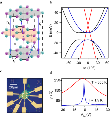
Fig. 1a shows the lattice structure of ABA-TLG with all the hopping parameters. We use Slonczewski-Weiss-McClure (SWMcC) parametrization of the tight binding model for ABA-TLG McCann and Fal’ko (2006); Koshino and McCann (2010) (with hopping parameters and ) to calculate its low energy bandstructure. Definitions of all the hopping parameters are evident from Fig. 1a and is the onsite energy difference of two inequivalent carbon atoms on the same layer. Its band structure, shown in Fig. 1b, consists of both monolayer-like (ML) linear and bilayer-like (BL) quadratic bands Serbyn and Abanin (2013); Morimoto and Koshino (2013).
Fig. 1c shows an optical image of the device where the ABA-TLG graphene is encapsulated between two hexagonal boron nitride (hBN) flakes Wang et al. (2013). Four probe resistivity () of the device is shown in Fig. 1d. The low disorder in the device is reflected in high mobility 500,000 cm2V-1s-1 on electron side and 800,000 cm2V-1s-1 on hole side; this leads to carrier mean free path in excess of m (Supplementary Information).
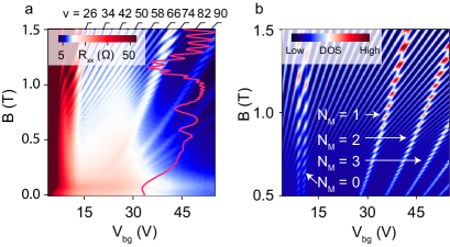
We next consider the magnetotransport in ABA-TLG that reveals the presence of LLs arising from both ML and BL bands. The LLs are characterized by the following quantum numbers: (i) () defines the LL index with M (B) indicating monolayer (bilayer)-like LLs (ii) + (-) denotes the valley index of the LLs (iii) () denotes the spin quantum number of the electrons. All the data shown in this paper, are taken at 1.5 K. Fig. 2a shows the measured longitudinal resistance (Rxx) as a function of gate voltage (Vbg) and magnetic field (B) in the low B regime (see Supplementary Information for more data). Observation of LLs up to very high filling factor = 118 confirms the high quality of the device. Along with the usual straight lines in the fan diagram, we find additional interesting parabolic lines which arise because of LL crossings. Fig. 2b shows the calculated non-interacting density of states (DOS) in the same parameter range which matches very well with the measured resistance. We find that the low B data can be well understood in terms of non-interacting picture and it allows determination of the band parameters.
We now consider the LL fan diagram for a larger range of Vbg and B. Fig. 3a shows the calculated Koshino and McCann (2010); McCann and Fal’ko (2006); Serbyn and Abanin (2013) energy dispersion of the spin degenerate LLs with B. We use zero electric field approximation (Supplementary Information) which is reasonable and consistent with experiment. All the band parameters of multilayer graphene are not known precisely, so, we refine the band parameters a little over the known values for bulk graphiteDresselhaus and Dresselhaus (2002) in order to understand our experimental data. We find = 3.1eV, = 0.39eV, = -0.028eV, = 0.01eV and = 0.021eV best describe our data. Fig. 3b shows the main fan diagram where the measured longitudinal conductance (Gxx) is plotted as a function of Vbg and B. Due to lack of inversion symmetry, valley degeneracy is not protected in ABA-TLG, it breaks up with increasing B and reveals all the symmetry broken filling factors as seen in Fig. 3b.
Fig. 3c shows measured Gxx focusing on the = 0 state, which shows a dip right at the charge neutrality point, evident for B 6 T. Corresponding transverse conductance (Gxy) shows a plateau at zero indicating the occurrence of the = 0 state. While, the = 0 plateau has been observed in monolayer graphene Zhang et al. (2006) and in bilayer graphene Zhao et al. (2010) (for B more than 15 T - 25 T), this is the first observation of = 0 state in trilayer graphene at such a low B. A marked reduction in disorder allows observation of the = 0 state in our device.
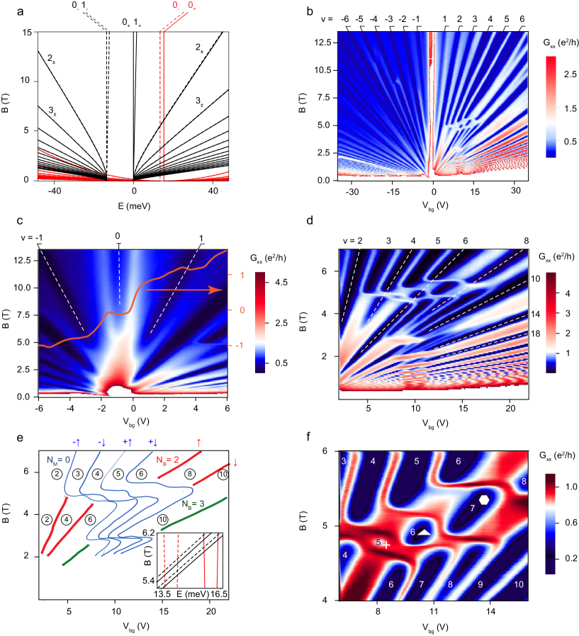
Focusing on the electron side, Fig. 3d and 3e show the experimentally measured LL fan diagram and labelled LLs, respectively. We see that the presence of LL gives rise to a series of vertical crossings along the B axis as is expected from the LL energy diagram (Fig. 3a). The highest crossing along the B axis appears when crosses with LL at T.
From the complex fan diagram, seen in Fig. 3d and 3e, we can see both above and below the topmost LL crossing (10 V and 5 T), LL is completely symmetry broken and LL quartet on the other hand becomes two fold split at 3.5 T. The crossing between NM = 0 and NB = 2 LLs gives rise to three ring-like structures. Calculated LL energy spectra near the topmost crossing (Fig. 3e inset) shows that spin splitting is larger than valley splitting for LL but valley splitting dominates over spin splitting for LL. We note that valley splitting of = 0 is very large compared to other ML LLs; which arises because ML bands are gapped in ABA-TLG unlike in monolayer graphene. As one follows the LL down towards B = 0 one observes successive LL crossings of with 2,3,4 ….. The sharp abrupt bends in the fan diagram occur due to the change of the order of filling up of LLs after crossings and the fact that the horizontal axis is charge density (proportional to and not LL energy). When these crossings are extrapolated to , we see that LL is valley split as expected from the LL energy diagram Fig. 3a.
We next discuss experimental signatures that point towards the importance of interaction. Observation of spin split NM = 0 LL at B 2 T cannot be explained from the non-interacting Zeeman splitting for 1.5 meV on electron side, estimated from the Dingle plot. Also, large ratio of transport scattering time () to quantum scattering time ()( 49) indicates that small angle scattering is dominant, a signature of the long range nature of the Coulomb potential Hwang and Das Sarma (2008); Coleridge (1991); Knap et al. (2004) (Supplementary Information). We also measure activation gap for the symmetry broken states at B = 13.5 T, and find significantly higher gaps than the non-interacting spin-splitting. For and 5, Fermi energy (EF) lies in spin polarized gap of NM = 0 LL in K- and K+ valley respectively. Measured energy gap at is 5.1 meV and at is 2.8 meV whereas free electron Zeeman splitting is 1.56 meV at B = 13.5 T (Supplementary Information). We note that typically the transport gap tends to underestimate the real gap due to the LL broadening, so actual single particle gap might be even larger.
Interaction results in symmetry broken states at low B that are QHF states. For the data in Fig. 3d, = 2,3,4,5 are QHF states for T. Similarly, 7,8,9 are also QHF states for 5.5 T 4 T. In fact the LLs associated with 3,4,5 after crossing are the same ML LLs which are responsible for 7,8,9 before crossing (Fig. 3e). The crossings result in three ring-like structures marked by , and in Fig. 3f.
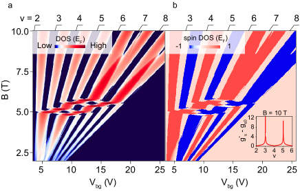
Now we discuss theoretical calculations to show that electronic interactions are crucial in obtaining a quantitative understanding of the experimental data. The theoretical calculations focus on the and LLs, which form the most prominent LL crossing pattern in our data. The effect of disorder is incorporated within a self-consistent Born approximation (SCBA) Ando (1974); Zheng and Ando (2002), while electronic interactions are included by considering the exchange corrections to the LL spectrum due to a statically screened Coulomb interaction Ando and Uemura (1974); Gorbar et al. (2012) in a self-consistent way. Fig. 4a shows the DOS at EF as a function of Vbg and , which matches with the experimental results on the Gxx.
Our calculations also provide insight about the polarization of the states inside the ring-like structures (Fig. 3f). We find that although the filling factor of region is the same as that of regions = 6 above and below, electronic configurations of these states are different. Fig. 4b shows the spin-resolved DOS at EF as a function of Vbg and . We find total spin polarization (integrated spin DOS) in region is non zero (Supplementary Information), but it vanishes in regions = 6 above and below the ring structure. Fig. 4b inset shows the calculated exchange enhanced spin g-factors. This shows significant increase over bare value of g in the spin polarized states – in agreement with the large gap observed at = 3 and 5 in experiment.
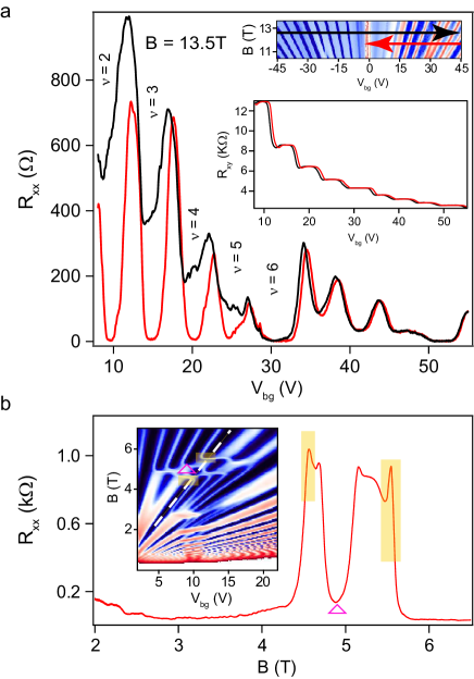
The key role of interactions is also reflected in the hysteresis of in the vicinity of the symmetry broken QHF states. QHF has been studied in 2DES using semiconductors Eom et al. (2000); Poortere et al. (2000) and in monolayer graphene Nomura and MacDonald (2006); Young et al. (2012). We vary filling factor by changing Vbg at a fixed B (Fig. 5a) and observe that the sweep up and down of Vbg shows a hysteresis in which can be attributed to the occurrence of pseudospin magnetic order at the symmetry broken filling factors Piazza et al. (1999) (see Supplementary Information for hysteresis data at = 7,8,9 at 3.5 T). Corresponding hysteresis is absent in simultaneously measured (Fig. 5a inset). Hysteresis in with Vbg is also absent without B (Supplementary Information). The pinning, that causes the hysteresis could be due to residual disorder within the system as the domains of the QHF evolve. Transport measurements show appearance of spikes around the crossing of NM = 0 and NB = 2 LLs (Fig. 5b). One possible explanation of the spike in Rxx Muraki et al. (2001) is the edge state transport along domain wall boundaries as studied earlier in semiconductors Poortere et al. (2000); Jungwirth and MacDonald (2001).
In summary, we see interaction plays an important role to enhance the g-factor and favours the formation of QHF states at low B and at relatively higher temperature. ABA-TLG is the simplest system that has both massless and massive Dirac fermions, giving rise to an intricate and rich pattern of LLs that, through their crossings, can allow a detailed study of the effect of interaction at sufficiently low temperature. The ability to image these QHF states using modern scanning probe techniques at low magnetic fields could provide insight into these states that have never been imaged previously. In future, experiments on multilayer graphene, exchange coupled with a ferromagnetic insulating substrate Wang et al. (2015), can lead to the possibility of observing interesting interplay of QHF with the proximity induced ferromagnetic order.
Acknowledgements
We thank Allan MacDonald, Jainendra Jain, Jim Eisenstein, Fengcheng Wu, Vibhor Singh, Shamashis Sengupta, Chandni U. for discussions and comments on the manuscript. We also thank John Mathew, Sameer Grover and Vishakha Gupta for experimental assistance. We acknowledge Swarnajayanthi Fellowship of Department of Science and Technology (for MMD) and Department of Atomic Energy of Government of India for support. Preparation of hBN single crystals are supported by the Elemental Strategy Initiative conducted by the MEXT, Japan and a Grant-in-Aid for Scientific Research on Innovative Areas “Science of Atomic Layers” from JSPS.
Author Contributions
B.D. fabricated the device, conceived the experiments and analysed the data. M.M.D., A.B. and B.D. contributed to development of the device fabrication process. K. W and T. T. grew the hBN crystals. S.D., A.S. and B.D. did the calculations under the supervision of R.S. B.D. and M.M.D co-wrote the manuscript, R.S. provided input on the manuscript. All authors commented on the manuscript. M.M.D supervised the project.
References
- Yacoby (2011) A. Yacoby, Nature Physics 7, 925 (2011).
- Taychatanapat et al. (2011) T. Taychatanapat, K. Watanabe, T. Taniguchi, and P. Jarillo-Herrero, Nature Physics 7, 621 (2011).
- Bao et al. (2011) W. Bao, L. Jing, J. V. Jr, Y. Lee, G. Liu, D. Tran, B. Standley, M. Aykol, S. B. Cronin, D. Smirnov, M. Koshino, E. McCann, M. Bockrath, and C. N. Lau, Nature Physics 7, 948 (2011).
- Kumar et al. (2011) A. Kumar, W. Escoffier, J. M. Poumirol, C. Faugeras, D. P. Arovas, M. M. Fogler, F. Guinea, S. Roche, M. Goiran, and B. Raquet, Physical Review Letters 107, 126806 (2011).
- Zhang et al. (2012) F. Zhang, D. Tilahun, and A. H. MacDonald, Physical Review B 85, 165139 (2012).
- Henriksen et al. (2012) E. Henriksen, D. Nandi, and J. Eisenstein, Physical Review X 2, 011004 (2012).
- Craciun et al. (2009) M. Craciun, S. Russo, M. Yamamoto, J. B. Oostinga, A. Morpurgo, and S. Tarucha, Nature nanotechnology 4, 383 (2009).
- Campos et al. (2016) L. C. Campos, T. Taychatanapat, M. Serbyn, K. Surakitbovorn, K. Watanabe, T. Taniguchi, D. A. Abanin, and P. Jarillo-Herrero, Phys. Rev. Lett. 117, 066601 (2016).
- Lee et al. (2013) Y. Lee, J. Velasco Jr, D. Tran, F. Zhang, W. Bao, L. Jing, K. Myhro, D. Smirnov, and C. N. Lau, Nano letters 13, 1627 (2013).
- Stepanov et al. (2016) P. Stepanov, Y. Barlas, T. Espiritu, S. Che, K. Watanabe, T. Taniguchi, D. Smirnov, and C. N. Lau, arXiv:1607.03635 [cond-mat] (2016), arXiv: 1607.03635.
- Serbyn and Abanin (2013) M. Serbyn and D. A. Abanin, Physical Review B 87, 115422 (2013).
- Poortere et al. (2000) E. P. D. Poortere, E. Tutuc, S. J. Papadakis, and M. Shayegan, Science 290, 1546 (2000).
- Jungwirth and MacDonald (2001) T. Jungwirth and A. H. MacDonald, Physical Review Letters 87, 216801 (2001).
- Girvin (2007) S. M. Girvin, Physics Today 53, 39 (2007).
- Eom et al. (2000) J. Eom, H. Cho, W. Kang, K. L. Campman, A. C. Gossard, M. Bichler, and W. Wegscheider, Science 289, 2320 (2000).
- McCann and Fal’ko (2006) E. McCann and V. I. Fal’ko, Phys. Rev. Lett. 96, 086805 (2006).
- Koshino and McCann (2010) M. Koshino and E. McCann, Physical Review B 81, 115315 (2010).
- Morimoto and Koshino (2013) T. Morimoto and M. Koshino, Physical Review B 87, 085424 (2013).
- Wang et al. (2013) L. Wang, I. Meric, P. Y. Huang, Q. Gao, Y. Gao, H. Tran, T. Taniguchi, K. Watanabe, L. M. Campos, D. A. Muller, J. Guo, P. Kim, J. Hone, K. L. Shepard, and C. R. Dean, Science 342, 614 (2013).
- Dresselhaus and Dresselhaus (2002) M. S. Dresselhaus and G. Dresselhaus, Advances in Physics 51, 1 (2002).
- Zhang et al. (2006) Y. Zhang, Z. Jiang, J. P. Small, M. S. Purewal, Y.-W. Tan, M. Fazlollahi, J. D. Chudow, J. A. Jaszczak, H. L. Stormer, and P. Kim, Phys. Rev. Lett. 96, 136806 (2006).
- Zhao et al. (2010) Y. Zhao, P. Cadden-Zimansky, Z. Jiang, and P. Kim, Phys. Rev. Lett. 104, 066801 (2010).
- Hwang and Das Sarma (2008) E. H. Hwang and S. Das Sarma, Phys. Rev. B 77, 195412 (2008).
- Coleridge (1991) P. T. Coleridge, Physical Review B 44, 3793 (1991).
- Knap et al. (2004) W. Knap, V. I. Fal’ko, E. Frayssinet, P. Lorenzini, N. Grandjean, D. Maude, G. Karczewski, B. L. Brandt, J. Lusakowski, I. Grzegory, M. Leszczynski, P. Prystawko, C. Skierbiszewski, S. Porowski, X. Hu, G. Simin, M. A. Khan, and M. S. Shur, Journal of Physics: Condensed Matter 16, 3421 (2004).
- Ando (1974) T. Ando, Journal of the Physical Society of Japan 36, 1521 (1974).
- Zheng and Ando (2002) Y. Zheng and T. Ando, Phys. Rev. B 65, 245420 (2002).
- Ando and Uemura (1974) T. Ando and Y. Uemura, Journal of the Physical Society of Japan 37, 1044 (1974).
- Gorbar et al. (2012) E. V. Gorbar, V. P. Gusynin, V. A. Miransky, and I. A. Shovkovy, Phys. Rev. B 85, 235460 (2012).
- Nomura and MacDonald (2006) K. Nomura and A. H. MacDonald, Physical Review Letters 96, 256602 (2006).
- Young et al. (2012) A. F. Young, C. R. Dean, L. Wang, H. Ren, P. Cadden-Zimansky, K. Watanabe, T. Taniguchi, J. Hone, K. L. Shepard, and P. Kim, Nature Physics 8, 550 (2012).
- Piazza et al. (1999) V. Piazza, V. Pellegrini, F. Beltram, W. Wegscheider, T. Jungwirth, and A. H. MacDonald, Nature 402, 638 (1999).
- Muraki et al. (2001) K. Muraki, T. Saku, and Y. Hirayama, Physical Review Letters 87, 196801 (2001).
- Wang et al. (2015) Z. Wang, C. Tang, R. Sachs, Y. Barlas, and J. Shi, Phys. Rev. Lett. 114, 016603 (2015).