Phonon assisted resonant tunnelling and its phonons control
Abstract
We observe a series of sharp resonant features in the tunnelling differential conductance of InAs quantum dots. We found that dissipative quantum tunnelling has a strong influence on the operation of nano-devices. Because of such tunnelling the current-voltage characteristics of tunnel contact created between atomic force microscope tip and a surface of InAs/GaAs quantum dots display many interesting peaks. We found that the number, position, and heights of these peaks are associated with the phonon modes involved. To describe the found effect we use a quasi-classical approximation. There the tunnelling current is related to a creation of a dilute instanton-anti-instanton gas. Our experimental data are well described with exactly solvable model where one charged particle is weakly interacting with two promoting phonon modes associated with external medium. We conclude that the characteristics of the tunnel nanoelectronic devices can thus be controlled by a proper choice of phonons existing in materials, which are involved.
I Introduction
One of the practical problems in semiconductor tunnel nanoelectronics is to extend control over parameters of quantum tunnel effect of electrons [2, -19, ]. Physical and chemical approaches to electron transfer processes at nanoscales reveal some common tools. Namely, analytical models of multidimensional dissipative simultaneous quantum tunneling of one or two charged particles, electrons or protons, in low-dimensional systems used in studying some chemical reactions at low temperatures [9, -Dakhnovskii88, ], can be used to study physical properties of quantum dots (QDs) [10, ], [20, -22, ].
Quasiclassical, dilute instanton-antiinstanton gas approach to the dissipative quantum tunneling of particles interacting with heat bath is known to be powerful technique in obtaining analytical results, starting from a classical action of the system [2, -4, ]. In particular, probability rate of quantum tunneling of two mutually interacting charged particles moving in medium, which occurs in synchronous or asynchronous modes, was studied in our previous work [7, ].
The purpose of the present work is to identify experimentally observed dissipative tunneling effects predicted by the theory developed in the pioneering works of A.J. Leggett, A.I. Larkin, Yu.N. Ovchinnikov et al. In this paper, we show results of our recent experimental study of the effect of wide-band matrix on semiconductor InAs/GaAs(001) QDs which changes some macroscopic properties of the system, and can be identified by the tunnel current-voltage (I—V) relationship of the tunnel device. Parameter associated to this effect can be treated as one more controllable parameter of nanostructures, in addition to energy levels of QD which are controlled by its size parameter. Note that the role of wide-band matrix in taking control over mesoscopic systems has been stressed in [1, ]. Also, we develop and apply 1D dissipative tunneling model accounting for influence of two promoting phonon modes coming from the wide-band matrix, to study quantum tunneling in the structure of single QDs by Conducting Atomic Force Microscopy (CAFM). We make a comparison of the obtained theoretical tunneling probability rate in an oscillatory regime with the experimental I—V relationship of the contact between Atomic Force Microscopy (AFM) probe and InAs/GaAs(001) QD surface.
II 1D dissipative tunneling probability rate with account for two local phonon modes in the wide-band matrix
We start by short description of the dissipative tunneling approach, which will be used in formulating our specific model. Let is the momentum of the tunneling particle, is the coordinate of the the tunneling particle, is the two-well potential. Then the Hamiltonian
| (1) |
describes particle in the model asymmetric two-well oscillatory potential along the tunnel coordinate . In Eq.(1) are momenta of phonon modes of the particle of mass , are coordinates of local phonon modes, are frequencies of local phonon modes, is the number of local modes of wide-band matrix, and are coefficients of the interaction of the tunneling particle with local phonon modes of wide-band matrix (see [13, , 7, ,Dakhnovskii88, ] for more details).

The quasiclassical action of the system is defined by [7, ]
| (2) |
Hereafter, dot denotes derivative over , is the inverse temperature, is the Matsubara Green’s functions [2, ,3a, ], , , and we introduced the renormalized potential
| (3) |
The form of the potential as a function of the renormalized coordinate is shown in Fig. 1. The procedures of the renormalization of the potential and the coordinate are considered in [Dakhnovskii88, ].
In the instanton approximation, 1D Euclidean action for one charged particle in the two-well renormalized oscillator potential and the external electric field is found as [13, , 14, , 20, ]
| (4) |
where is charge of the particle, and are parameters of the renormalized two-well potential in the external electric field , are positions of the minima of the potential in zero-field case, is the instanton center, is the oscillator potential frequency, is Matsubara frequency, , and is the Fourier component of the viscous core of the corresponding quasiclassical Euler-Lagrange equation of motion,
| (5) |
The probability of quantum tunneling of the particle through the barrier shown in Fig.1 per unit time contains pre-exponential factor , the most contribution to which is made by the particle trajectories that are very close to the instanton. Expanding the action up to quadratic term in , where is the extremal instanton trajectory, and integrating over the functional space, we get
| (6) |
where
| (7) |
Here, denotes determinant with zero eigenvalues corresponding to zero modes of the instanton omitted, and we used the approximation of dilute instanton-antiinstanton gas, i.e., the probability rate is much smaller than the inverse width of instanton,
| (8) |
We assume that the major contribution to the action is made by the instanton, i.e., by the trajectory , which minimizes the action (4) and obeys the following Euler-Lagrange equation:
| (9) |
Here, the trajectory is found within the class of periodic functions . The form of the solution of Eq.(9) obeying this condition is shown in Fig. 2.

With the action (4), we obtain from Eq. (6) as follows:
| (10) |
Now, we specify our model by assuming that the particle interacts weakly with two local phonon modes, i.e., and .
We also make natural assumption that the interactions are weak, i.e., and . In this case, we get
| (11) |
The tedious calculations provides an analitic formulae for the optimal action and pre-exponetial factor . Due its large expression it is given in [Suppl, ]. For a completeness, we should mention that there is a second solution which corresponds to the case of non-oscillating character of the probability rate. We shortly present the results for this case in [Suppl, ].
III Experimental setup
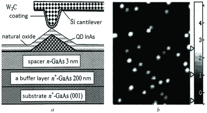
The experimental setup is shown in Fig. 3. Samples for the study were prepared on the n+-GaAs(001) substrate doped by Sn using Metalorganic Hydridechemical Vapor Deposition (MOCVD) at atmospheric pressure.
The n+-GaAs buffer layer of 200 nm thickness doped by Si, with the donor concentration cm-3 has been grown at C. The n-GaAs spacer layer, with cm-3, of 3 nm thickness has been grown on the buffer layer. This layer forms triangular potential barrier between the QD and n+-GaAs buffer layer [25, ]. InAs QD has been formed by Stransky-Krastanov mechanism at C. Nominal thickness of deposited InAs layer is about 1.5 nm.
The samples have been prepared in Physical-Technical Research Institute, Nizhniy Novgorod University, Russia, and then used to study spatial and energy distribution of the local density of states in InAs QD by the method of tunnel AFM, in Kazan Physical-Technical Research Institute, Kazan, Russia.
Note that in [11a, ] local density of states in InAs/GaAs(001) QDs was measured by CAFM. In [11c, ], Scanning Tunneling Microscopy (STM) has been used in Ultra-High Vacuum (UHV) to measure local density of states in quantum wells GaSb/InAs. In [11b, ], combined UHV STM/AFM has been implemented for the first time for the tunneling spectroscopy of the size-quantized states in the InAs/ GaAs (001) surface QDs. Tunneling spectra and current images, which reflect the energy and spatial distribution of the local density of the ground and excited states in the QDs have been obtained. Tunneling AFM technique and results of ex situ investigations of local density of states of quantum confined states in self-assembled semiconductor InAs/GaAs(001) QDs and InGaAs/GaAs InAs/GaAs(001) quantum rings, grown by Atmospheric Pressure Metal Organic Vapour Phase Epitaxy (AP-MOVPE), and GeSi/Si InAs/GaAs(001) nanoislands covered by native oxide have been presented in [23, ]. There, samples with surface nanostructures were scanned across by conductive Si AFM probe covered by conductive coating (Pt, W2C, or diamond-like film) in the contact mode. Main advantage of the tunneling AFM as compared to UHV STM is that the former allows ex situ investigation of the surface semiconductor nanostructures, which are naturally oxidized in ambient air when one takes samples from growth setup to AFM setup.
Our experiment was done at room temperatures, under very high vacuum in the camera, by scanning probe microscope Omicron UHV AFM/STM VT which is a part of very high vacuum set up Omicron MultiProbe P. Basic pressure in the camera was about 10-10 Torr. Surface of the sample experienced oxidation in ambient air during the time of transportation from the growth set up to the vacuum camera. It was scanned by p+-Si probe with W2C covering, in contact mode (see Fig. 3), with potential difference between n+-GaAs substrate and AFM probe.
In the experiment, we have obtained spatial distributions of electric current between AFM probe and the sample as a function of AFM probe coordinates in the plane of sample’s surface, at various constant . We refer to these distributions as current images. They reflect spatial distribution of local density of states in the plane: wave function mappings [11c, ] with a sum over energies below Fermi level of the probe. We do not present resulting current images here, and mention only that for the potential difference range V across it, these reveal two maxima corresponding to -symmetry of the excited states of QDs, while at lower voltages V the current images have round form corresponding to the -symmetry of the ground state [24b, ].
I—V relationship of the contact between the AFM probe and QD have been obtained by measuring current images at different fixed . More details on the used method of growth and tunnel spectroscopy of QD one can find, e.g., in [24, ].
Fig.3b represents AFM image of the surface of the studied sample. surface QD has 5 to 6 nm thickness. It should be noted that lateral dimensions of QD shown in Fig.3b are significantly larger than that expected for QD, 10 to 12 nm, which has form of tetrahedral pyramid with planes (101). This is explained by the effect of convolution related to the curvature of the AFM probe characterized by the radius nm.
IV Comparison with the experiment
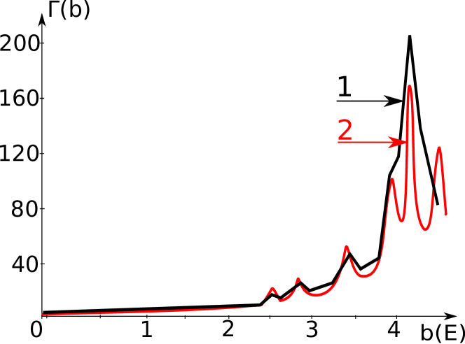
We turn to a comparison of the obtained theoretical results for the 1D quantum tunneling probability rate of the charged particle weakly interacting with the two local phonon modes of medium with the experimental I—V relationship of InAs/GaAs(001) QD measured by using CAFM.
In Fig. 4, we plot the experimental I—V relationship and the obtained result for tunneling probability rate , which we treat as proportional to the current , as a function of the parameter linearly depending on the external electric field intensity , which in turn linearly depends on the potential difference across it.
Fitting parameters are the frequencies of local phonon modes and the coupling constants of the particle to these modes. Values of other parameters of the model, namely, the two-well potential parameters, temperature, and external electric field intensity were set due to the experiment.
The observed peaks are not due to Coulomb blockage because these are not equidistant. Sometimes these peaks are interpreted as the result of a resonance phenomenon in tunneling.
While the position of the highest theoretical peak meets the experimental one, its height underestimates the latter by about 20%. Also, we note that the highest experimental peak reveals signs of two additional peaks matching two theoretical ones close to the highest peak. This can be explained by an approximate character of the used asymmetric two-well oscillatory potential.
The case of non-oscillating character of the probability rate obviously does not correspond to the experimental data. Nevertheless, we present shortly the results in Supplemental Material [Suppl, ]. This damping solution is valuable as it tells us that whether the rate is of oscillating or non-oscillating character depends on the temperature, external electric field intensity , and type of wide-band matrix, which carries studied QDs.
V Conclusions
Our measurements reveal a rich spectrum of inelastic phonon-assisted electron tunneling processes in InAs/GaAs quantum dots. The number, position, and heights of the resonant peaks observed is well described with developed instanton approach extended to include effects of dissipative quantum tunneling. The good agreement with experiments have been achieved using a model in which an inelastic tunneling transition becomes allowed. There in the model of the wide-band matrix of InAs/GaAs quantum dots two phonon modes have been taken into account. The comparison between the experiments and developed theory allows us to probe electron-phonon interactions in this system and identify spectroscopically the energies and nature of the phonons emitted during the tunnelling.
Practical implication of the obtained result is that the current-voltage characteristics of the semiconductor tunnel nanoelectronic devices can thus be controlled to a certain extent by modulations of the wide-band matrix parameters. For example, the quantum dots can serve as very sensitive detectors of properties of bulk materials used in precision nanoelectronics.
It is necessary to note that the theory for dissipative tunneling with the influence of two local phonon modes in the external electric field developed in this paper can be used in problems of resonant impurity states in quantum molecules in the case when the lifetime of the impurity electron is mainly determined by electron tunneling decay.
The problem of the influence of the electric field on the radiative recombination spectra of electrons and holes in a quantum dot is also of interest [Zegrya2006, -Zegrya2009, ]. In this case the electron tunneling between a quantum dot and biological object can play an important role.
A.K.A., M.B.S., and V.D.K. are grateful to Committee of Science of the Ministry of Education and Science of Kazakhstan for a partial financial support under the grant. The part of this work was done in the framework of the state contract by Ministry of Education and Science of the Russian Federation. The authors are also grateful to A. J. Leggett for his attention to this work; to B.N. Zvonkov, Research Institute for Physics and Technology, N.I. Lovachevskii University of Nizhny Novgorod, for QD samples used in CAFM experiment; to P.A. Borodin for assistance in carrying out CAFM experiment, and to I.E. Bulyzhenkov and Yu.N. Ovchinnikov for useful discussions.
References
- (1) A.O. Caldeira and A.J. Leggett, Phys. Rev. Lett. 46, 211 (1981).
- (2) A.I. Larkin and Yu.N. Ovchinnikov, JETP Lett. 37, 322 (1983).
- (3) I.E. Bulyzhenkov and B.I. Ivlev, JETP 47, 115 (1978).
- (4) A.I. Larkin and Yu.N. Ovchinnikov, JETP 91, 318 (1986).
- (5) Y. Imry, Introduction to Mesoscopic Physics, Oxford University Press, Oxford, 2008.
- (6) Transfer Processes in Low-Dimensional Systems (collection of articles, which is dedicated to the prof. A.A. Ovchinnikov and prof. A.I. Larkin s memory), ed. by Yu.I. Dahnovsky, V.D. Krevchik, V.Ya. Krivnov, M.B. Semenov, and K. Yamamoto, UT Research Institute Press, Tokyo (2005).
- (7) Controllable Dissipative Tunneling. Tunneling Transport in Low-Dimensional Systems, ed. by A. J. Leggett et al., Fizmatlit, M. (2012).
- (8) A. Venkatesan, K.J. Lulla, V.J. Patton, A.D. Armour, C.J. Mellor, and J.R. Owers-Bradley, Phys. Rev. B 81, 073410 (2010).
- (9) Yu. Bomze, H. Mebrahtu, I. Borzenets, A. Makarovski, and G. Finkelstein, Phys. Rev. B 79, 241402(R) (2009).
- (10) D.K. Ferry, S.M. Goodnick, and J. Bird, Transport in Nanostructures, Cambridge University Press, Cambridge, 2009.
- (11) L.G.G.V. Dias da Silva and E. Dagotto, Phys. Rev. B 79, 155302 (2009).
- (12) A. Grodecka, P. Machnikowski, and J. Forstner, Phys. Rev. B 78, 085302 (2008).
- (13) Yu. Dahnovsky, A.A. Ovchinnikov, and M.B. Semenov, JETP 92, 955 (1987).
- (14) Yu.I. Dahnovsky and M.B. Semenov, Journal of Chemical Physics 91, 7606 (1989).
- (15) V.F. Gantmakher and M.V. Feigel’man, Physics-Uspekhi 41, 105 (1998).
- (16) A.K. Aringazin, Yu. Dahnovsky, V.D. Krevchik, M.B. Semenov, A.A. Ovchinnikov, and K. Yamamoto, Phys. Rev. B 68, 155426 (2003).
- (17) Yu.I. Dahnovsky, A.A. Ovchinnikov and M.B. Semenov, Molecular Physics 63, 497 (1988).
- (18) V.Ch. Zhukovsky, O.N. Gorshkov, V.D. Krevchik, M.B. Semenov, E.V. Groznaya, D.O. Filatov, and D.A. Antonov, Moscow University Physics Bulletin 64, 27 (2009).
- (19) V.Ch. Zhukovsky, Yu. I. Dahnovsky, O.N. Gorshkov et al. (Collaboration), Moscow University Physics Bulletin 64, 475 (2009).
- (20) V.Ch. Zhukovsky, Yu. I. Dahnovsky, V.D. Krevchik, M.B. Semenov, V.G. Mayorov, E.I. Kudryashov, E.V. Shcherbakov, and K. Yamamoto, Moscow University Physics Bulletin 62, 73 (2007).
- (21) See Supplemental material for this paper.
- (22) A.A. Bukharaev, N.V. Berdunov, D.V. Ovchinnikov, and K.M. Salikhov, Russian Microelectronics 26, 137 (1997).
- (23) K.M. Lang, D.A. Hite, R.W. Simmonds, R.Mc. Dermott, D.P. Pappas, and J.M. Martinis, Review of Scientific Instruments 75, 2726 (2004).
- (24) K. Suzuki, K Kanisawa, C. Janer, S. Perraud, K. Takashina, T. Fujisawa, and Y. Hirayama, Phys. Rev. Lett. 98, 136802 (2007).
- (25) P.A. Borodin, A.A. Bukharaev, D.O. Filatov, D.A. Vorontsov, and M.A. Lapshina, J. Surf. Investigations: X-ray, Synchrotron, and Neutron Techniques 3, 721 (2009).
- (26) D. Filatov, V. Shengurov, N. Nurgazizov, P. Borodin, and A. Bukharaev, in: Tunneling atomic force microscopy of self-assembled In(Ga)As/GaAS quantum dots and rings and of GeSi/Si (001) nanoislands, Fingerprints in the optical and transport properties of quantum dots, ed. by A. Al-Ahmadi, Published in Tech, Croatia (2012), pp.273-298.
- (27) O. Stier, M. Grundmann, and D. Bimberg, Phys. Rev. B 59, 5688 (1999).
- (28) T. Maltezopoulos, A. Bolz, Ch. Meyer, Ch. Heyn, W. Hansen, M. Morgenstern, and R. Wiesendanger, Phys. Rev. Lett. 91, 196804 (2003).
- (29) G. G. Zegrya. Tech. Phys. Lett. 32, 174 (2006).
- (30) G. G. Zegrya, D. M. Samosvat. JETP 108, 907 (2009).