A 50/50 electronic beam splitter in graphene nanoribbons as a building block for electron optics
Abstract
Based on the investigation of the multi-terminal conductance of a system composed of two graphene nanoribbons, in which one is on top of the other and rotated by , we propose a setup for a 50/50 electronic beam splitter that neither requires large magnetic fields nor ultra low temperatures. Our findings are based on an atomistic tight-binding description of the system and on the Green’s function method to compute the Landauer conductance. We demonstrate that this system acts as a perfect 50/50 electronic beam splitter, in which its operation can be switched on and off by varying the doping (Fermi energy). We show that this device is robust against thermal fluctuations and long range disorder, as zigzag valley chiral states of the nanoribbons are protected against backscattering. We suggest that the proposed device can be applied as the fundamental element of the Hong-Ou-Mandel interferometer, as well as a building block of many devices in electron optics.
Keywords: valleytronics, graphene, bilayer, beam splitter
1 Introduction
The realization of single electron sources [1, 2], where electrons are injected on-demand and propagate coherently in a conductor, has open the possibility of exploring very interesting new quantum information processing ideas using quantum coherent electronics. In particular, analogies between single-particle electron and photon propagation triggered several beautiful electron transport experiments inspired on optical setups [3, 4, 5, 6, 7, 8, 9, 10, 11].
Currently, the most successful platform for experiments with single-electron sources relies on the quantum Hall regime. One of the main reasons are the electronic edge states characteristic of the quantum Hall regime. Those are one-dimensional states with a given chirality, which protects them from electronic backscattering [12, 13], improving electronic transport of nanodevices and making possible to develop electronic interferometric devices. Indeed, electronic analogues of many optical devices such as Mach-Zehnder [3, 4, 5, 6, 7], Fabry-Perot [8, 9], and Hanbury Brown-Twiss [10, 11] have been implemented in recent years in Quantum Hall systems. These devices are not only important for the investigation of fundamental coherent electronic transport but also to applications in quantum computation [14]. In these devices the mixing of these chiral edge states have been realized using beam splitters based on quantum point contracts. Coherent beam splitters for electrons have been implemented by means of quantum dots with normal [15, 16, 17] and superconducting contacts [18]. However, we emphasize that chiral states in Quantum Hall systems can only occur at high magnetic fields and low temperatures, a fact that hampers the development of practical devices and technologies.
In order to circumvent these practical limitations, alternative physical concepts have been employed in recent years to engineer electronic chiral states. Two-dimensional topological insulators that support symmetry protected chiral states [19, 20] have been proposed as suitable candidates, although the robust character of their edge states can be experimentally elusive [21, 22].
Among the materials exhibiting topological effects that support protected chiral states, graphene is one of the most versatile and useful for practical applications [23]. Of particular interest are graphene bilayers, which can exhibit interesting topological effects that have been proposed to give rise to a so-called valley Hall effect [24], that in monolayer graphene can be achieved by means of lattice deformations [25, 26]. Recently, two experimental groups [27, 28] succeeded in demonstrating that by changing the Berry curvature one can generate and control pure valley currents, the goal of valleytronics, in bilayer graphene.
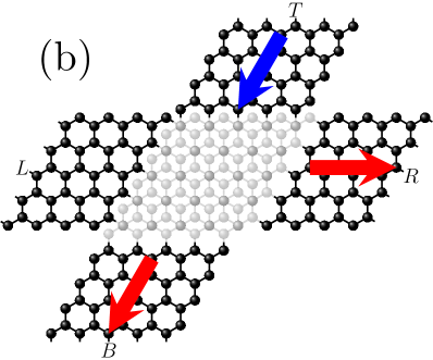
We adapt these ideas in a set up of two “crossed” graphene nanoribbons (GNRs), forming a four-terminal device, namely, a graphene bilayer central region coupled to 4 zigzag graphene leads. Those are possible to synthesize due to advances in bottom-up nanofabrication techniques, such as longitudinal unzipping of carbon nanotubes [29] and the assembling of carbon-based molecules [30, 31], that have allowed the production of GNRs with high-quality crystallographic edges. As a result, the state-of-the art nanofabrication technology can make possible experiments involving topological states in GNRs, many of them analogous to the ones conducted in quantum Hall systems [3, 4, 5, 6, 7, 8, 9, 10, 11] without the application of high magnetic fields.
In this paper we put forward a proposal for a 50/50 electronic beam splitter based on two GNRs, one on top of the other forming a four-terminal device as presented in what follows, as depicted in Fig. 1. We investigate the electronic transport in this system by means of a microscopic model based on the tight-binding approximation and the Landauer conductance formula. We demonstrate that it can be applied as a perfect 50/50 electronic beam splitter, in which its operation can be switched on and off by varying the electron doping. We show that this device is robust against thermal fluctuations and long range disorder, since zigzag valley dependent chiral modes of the nanoribbons are protected against backscattering [32, 33, 34]. We suggest that the proposed device can be applied as the fundamental element of the electronic analog [35] of the Hong-Ou-Mandel interferometer [36], as well as a building block of many devices in electron optics.
2 Model and theory
The model system we propose is composed of one zigzag GNR along the “horizontal” direction placed underneath another zigzag GNR, tilted by , as depicted in Fig. 1. The relative position and separation between the ribbon planes is such that the atoms at their intersection interact as in bilayer graphene with an - or -like stacking.
In graphene, orbitals of neighboring carbon atoms hybridize to allow for electronic conduction. The electronic model Hamiltonian of such a system reads
| (1) |
where () and () are the creation and annihilation operators of the electrons at the -th site of the sublattice (). The index labels the top () and the bottom () nanoribbons, whereas restricts the summations to intra- or interplane first neighbors sites. The first term accounts for the electronic hopping between nearest neighbors sites in the same plane with an intra-plane hopping integral eV. The second term includes the onsite energies of the -site in the plane on the sublattice () or (). We study cases where an external electric field is applied in the central region, defined as the intersection between ribbons (see Fig. 1), so that the potential energy in the ribbon planes is constant, . The interplane potential difference can be used as a handle to control the transport properties of the central region as it will be shown in the following. Finally, the last term accounts for the interplane hopping with hopping amplitude eV [23].
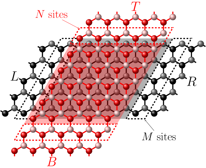
We use the Landauer approach suited for mesoscopic quantum coherent conductors to calculate the transport properties of the four-terminal system depicted in Fig. 1. We assume that the central region, indicated by the shaded area in Fig. 1, is connected by GNRs to electron reservoirs in equilibrium. The terminals are denoted by , corresponding to left, right, top and bottom leads, respectively.
For low bias, the linear conductance from terminal to is given by the Landauer formula [37], namely
| (2) |
where is the Fermi-Dirac distribution and is the transmission, that is calculated using the Caroli formula [38, 37]
| (3) |
where is the full retarded Green’s function of the central region and is the linewidth function of the lead (terminal) . The notation is standard, see for instance, Ref. [39] for a detailed description of these objects.
Let us briefly describe the numerical implementation of the transmission calculation. The horizontal and tilted ribbons have by sites in the central region. Hence, owing to the honeycomb lattice structure, the number of sites in each plane is . Thus the total number of sites in the central region is , which gives the dimension of its real space Green’s function. Using the first cell of right and top contacts indicated by the dashed lines in Fig. 1, we calculate the corresponding surface Green’s function by means of a decimation technique [39]. We obtain the surface Green’s functions of the remaining contacts by means of symmetry operations on the right and top contact Green’s functions. This simplifies the computation of the retarded self-energies and the line width functions . We calculate the retarded Green’s function of the central region by the (sparse) matrix inversion , where the total retarded self-energy is .
3 Results
Let us now show that by tuning the doping (Fermi energy) and the external electric field on the central region, the system introduced in Sec. 2 can be used to generate a 50/50 electronic beam splitter. Next, we discuss its application as a Hong-Ou-Mandel electron interferometer.
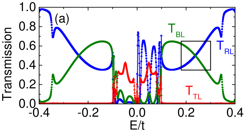
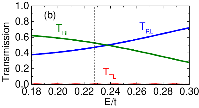
Figure 2 shows the transmission coefficients of electrons injected from the left arm of our model system (see Fig. 1) for electronic energies close to the charge neutrality point. The panel (a) shows the values of , and for . Figure 2 reveals that, for a wide energy range, the transmission is almost evenly distributed between the right and bottom arms. This is a result of the valley dependent chiral nature of the modes participating in the electronic transport in the zigzag GNRs. By setting eV, transmission in the top arm vanishes and the probability of transmission in both right and bottom arms is , as it can be seen in Fig. 2(b). In this regime the system works as a 50/50 electronic beam splitter where the voltage plays the role of a switch on/switch off external parameter. Experimentally, the voltage can be controlled by an external electric field and the Fermi energy or the doping is controlled by gate voltages. By tuning and , one can optimize the system operation parameters. Thermal fluctuations, due to temperatures up to K, do not affect the transport suppression to the top arm. Indeed, they hardly affect the transmission ratio between right and bottom contacts, which may reach values lesser than 60/40, as it can be seen in Fig. 2(b).
In addition, we have verified that if one injects electrons into the top arm , the transmission follows the same trend of Fig. 2, where electrons are injected in the left arm, provided we set the same values for the potential and the Fermi energy eV. In this case, transmission from the top arm to the left one is ; transmission from the top arm to the right one is ; and transmission from the top arm to the the bottom one is .
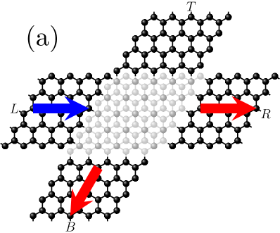
Figure 3 schematically shows the electronic propagation upon injection from both left and top arms. Hence, we have shown that by properly tuning the voltage and the Fermi energy , the system under investigation acts as 50/50 electronic beam splitter, which is a key element in many applications in electron optics.
This behavior can be understood as follows: In our proposal the crystallographic zigzag edges guarantee that the low energy pair of valley states in each nanoribbon propagate in opposite directions [32, 33, 34]. The central region composed by an AB-stacked bilayer graphene provides interplane scattering that preserves the valley index over a wide energy range. In diffusive systems it is standard to use topological arguments: Since the system geometry does not have inversion symmetry, the external perpendicular electric field gives rise to a local (massive) Dirac band structure with two valleys characterized by a non-zero Berry curvature with opposite signs (we note that in experiments [27, 28], inversion symmetry is broken by the substrate [40]). Hence, by applying a bias, the electrons at each valley drift in opposite directions [24]. Since we address the transport properties using the Landauer formula, there is no explicit in-plane electric field and the reasoning above does not apply [41].
In the system we propose, the electrons are injected in the central region through the zigzag leads. As a consequence, for a small doping (or ) such that only the single open mode operation is enabled, the injected electrons through one ribbon, Fig. 3(a), are always valley polarized [34] and, thus, have a preferential deflection direction when scattered by the bilayer region to the other ribbon.
By tuning and the electric field, one can find the optimal operation parameters for a 50/50 beam splitter, see Fig. 3(a). In such configuration, the incoming electron from one plane can only be scattered to a single state in the other plane with a given propagation direction. The system shows a chiral symmetry: for electrons injected at the top GNR, one obtains an identical effect as above, illustrated by Fig. 3(b). In our case, for instance, the propagation directions to and to have the same “valley chirality”, as verified by our numerical calculations.
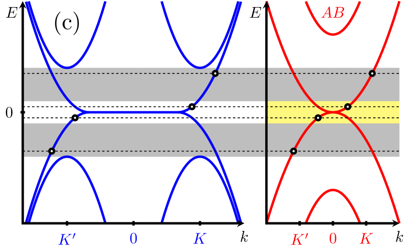
Let us discuss the simple case of with the help of Fig. 3(c). First we identify that the system in Fig. 1 is symmetric under rotation around a diagonal axis that takes the arm () into the arm (), interchanging top and bottom nanoribbons. The low energy electronic transport of each zigzag GNR is characterized by forward and backward moving states having opposite valley chirality [32, 33, 34]. Thus, assuming that the electrons injected in the system from the -arm are -polarized, the forward propagation to and the scattering to must be -polarized, while due to symmetry backscattering to and scattering to must be -polarized. For , away from the charge neutrality point as depicted in the upper gray area of Fig. 3(c), the electronic states in the bilayer region are fully -polarized and neither backscattering to nor propagation to is allowed. The same arguments apply to the negative energy region corresponding to the lower gray area. This explains the energy windows with no backscattering and zero transmission between and in Fig. 2. On the other hand, for energies near the charge neutrality point, the states in the bilayer region lie around having both and polarization components. Therefore, scattering to any of the four arms is allowed for, enabling backscattering to and propagation to , as seen in Fig. 2. For and/or for stacking, the picture is more complicated but the same line of arguments still holds.
As an example of application, let us discuss the employment of the electronic beam splitter in an alternative implementation of the Hong-Ou-Mandel effect for electrons [11, 2, 42]. For bosons, when two indistinguishable particles are incident on two separate input sides of a 50/50 beam splitter (BS), Bose-Einstein quantum statistics implies that the outgoing bosons must leave together in one of the two outputs. The coincidence counter placed at the outputs, that detects a signal when two particles strike both outputs at the same time, records zero coincidences. This effect, first observed for photons [43], leads to a vanishing coincidence for simultaneous photon injection, and it is characterized by a dip in the correlation function [36]. For electrons, in contrast, Fermi-Dirac statistics implies particle antibunching, so that two identical fermions simultaneously injected at two different terminals are always detected in different outputs, leading to a peak in the coincidence count [42].
The Hong-Ou-Mandel effect for single fermions was first observed in the one-dimensional edge states of quantum Hall systems [2], although previous measurements using continuous electronic beams have been reported [44, 11]. Proposals for the observation of the fermionic Hong-Ou-Mandel effect in graphene also exist [42].
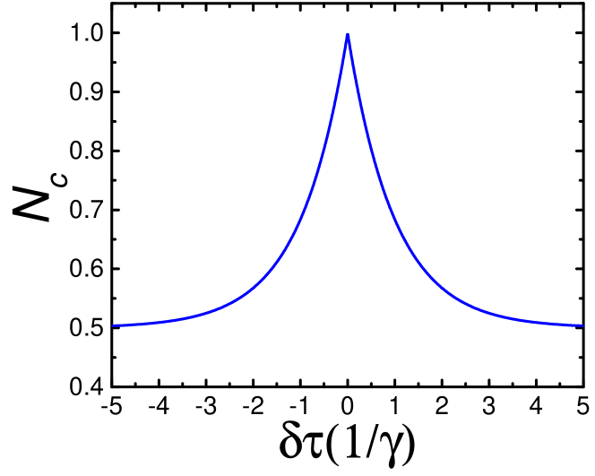
We propose that the Hong-Ou-Mandel effect can be verified in our system, depicted in Fig. 1, by using the terminals and as inputs and the terminals and as outputs. By tuning our system to work as a beam splitter in the regime shown in Fig. 2(b), the electrons injected from terminal () can be either transmitted to terminal () with transmission or “reflected” to terminal () with reflection . Note that a fine tuning can optimize the system to work as a 50/50 beam splitter where . If we introduce a delay time in the injection of one of the electrons and place a coincidence counter at the terminals and , the normalized coincidence count for our symmetric setup reduces to [42]
| (4) |
where is the characteristic time scale of the single electron transistor. In Fig. 4 the coincidence count is shown as a function of the delay time . It is clear from Fig. 4 that there is a peak at and for large , tends to a flat background, which corresponds to uncorrelated transport processes. From Eq. (4) one can verify that the maximum difference between the peak and the background occurs for , i.e. for a 50/50 beam splitter, as it is shown in Fig. 3.
This enhancement is precisely what can be achieved by the system proposed here with realistic parameters. In addition, the proposed system, based on the AB stacking of two GNRs, preserves the chirality of the states. As a result, electrons going from left arm to the right terminal have exactly the same chirality of an electron going from the top to the bottom arm. For this reason the AB staking guarantees that incoming electrons in the left lead will only exit the system through the right and bottom arms. The same happens for incoming electrons in the top arm (see Fig. 3(b)).
4 Conclusions
We have demonstrated that a system composed of zigzag GNRs, one rotated by on top of another, can function as an ideal 50/50 electronic beam splitter. We show that the operation of the beam splitter can be switched on and off by varying the value of the Fermi energy, which can be achieved by electrostatic gating. We also show that the operation of the proposed device is robust against thermal fluctuations. By making the nanoribbons wider one would change the energy scales of the system trivially. We speculate that our main findings still hold. Both and stackings of two GNRs preserve the valley polarization of the states. We argue that the valley polarization plays a central role in the beam splitter operation. We only presented results for stacking, but we have verified that the same conclusions also apply for the stacking.
We emphasize that the transmission for the first modes in zigzag GNRs is protected against backscattering due to long range disorder [32, 33, 34]. However, short range disorder, either due to edge roughness [45] or resonant scattering due to impurity adsorption at the system surface [46], is expected to be detrimental for an experimental realization of the proposed beam splitter. We also note that the presence of short ranged impurities in the central region give rise to intervalley scattering, which destroys the valley polarization. Recent experiments report an exponential decay of valley currents on the scale of microns [27, 28, 47]. In such scenario, finding the conditions of and for a proper operation can be challenging.
We suggest that the proposed device can be applied as the fundamental element of the Hong-Ou-Mandel interferometer, as well as a building block of many devices in electron optics.
References
- [1] G. Fève, A. Mahé, J.-M. Berroir, T. Kontos, B. Plaçais, D. C. Glattli, A. Cavanna, B. Etienne, and Y. Jin. An on-demand coherent single-electron source. Science, 316(5828):1169–1172, 2007.
- [2] E. Bocquillon, V. Freulon, J.-M Berroir, P. Degiovanni, B. Plaçais, A. Cavanna, Y. Jin, and G. Fève. Coherence and indistinguishability of single electrons emitted by independent sources. Science, 339(6123):1054–1057, 2013.
- [3] Yang Ji, Yunchul Chung, D. Sprinzak, M. Heiblum, D. Mahalu, and Hadas Shtrikman. An electronic mach-zehnder interferometer. Nature, 422(6930):415–418, Mar 2003.
- [4] I. Neder, M. Heiblum, Y. Levinson, D. Mahalu, and V. Umansky. Unexpected behavior in a two-path electron interferometer. Phys. Rev. Lett., 96:016804, Jan 2006.
- [5] Preden Roulleau, F. Portier, D. C. Glattli, P. Roche, A. Cavanna, G. Faini, U. Gennser, and D. Mailly. Finite bias visibility of the electronic mach-zehnder interferometer. Phys. Rev. B, 76:161309, Oct 2007.
- [6] L. V. Litvin, H.-P. Tranitz, W. Wegscheider, and C. Strunk. Decoherence and single electron charging in an electronic mach-zehnder interferometer. Phys. Rev. B, 75:033315, Jan 2007.
- [7] L. V. Litvin, A. Helzel, H.-P. Tranitz, W. Wegscheider, and C. Strunk. Edge-channel interference controlled by landau level filling. Phys. Rev. B, 78:075303, Aug 2008.
- [8] D. T. McClure, Yiming Zhang, B. Rosenow, E. M. Levenson-Falk, C. M. Marcus, L. N. Pfeiffer, and K. W. West. Edge-state velocity and coherence in a quantum hall fabry-pérot interferometer. Phys. Rev. Lett., 103:206806, Nov 2009.
- [9] Yiming Zhang, D. T. McClure, E. M. Levenson-Falk, C. M. Marcus, L. N. Pfeiffer, and K. W. West. Distinct signatures for coulomb blockade and aharonov-bohm interference in electronic fabry-perot interferometers. Phys. Rev. B, 79:241304, Jun 2009.
- [10] M. Henny, S. Oberholzer, C. Strunk, T. Heinzel, K. Ensslin, M. Holland, and C. Schönenberger. The fermionic hanbury brown and twiss experiment. Science, 284(5412):296–298, 1999.
- [11] I. Neder, N. Ofek, Y. Chung, M. Heiblum, D. Mahalu, and V. Umansky. Interference between two indistinguishable electrons from independent sources. Nature, 448(7151):333–337, Jul 2007.
- [12] K. v. Klitzing, G. Dorda, and M. Pepper. New method for high-accuracy determination of the fine-structure constant based on quantized hall resistance. Phys. Rev. Lett., 45:494–497, Aug 1980.
- [13] D. J. Thouless, M. Kohmoto, M. P. Nightingale, and M. den Nijs. Quantized hall conductance in a two-dimensional periodic potential. Phys. Rev. Lett., 49:405–408, Aug 1982.
- [14] A. Sarkar, T. K. Bhattacharyya, and A. Patwardhan. Quantum logic processor: Implementation with electronic mach-zehnder interferometer. Appl. Phys. Lett., 88(21), 2006.
- [15] J. R. Petta, H. Lu, and A. C. Gossard. A coherent beam splitter for electronic spin states. Science, 327(5966):669–672, 2010.
- [16] W. D. Oliver, J. Kim, R. C. Liu, and Y. Yamamoto. Hanbury brown and twiss-type experiment with electrons. Science, 284(5412):299–301, 1999.
- [17] G. Sun, X. Wen, B. Mao, J. Chen, Y. Yu, P. Wu, and S. Han. Tunable quantum beam splitters for coherent manipulation of a solid-state tripartite qubit system. Nat. Commun., 1(51), 2010.
- [18] L. Hofstetter, S. Csonka, J. Nygård, and C. Schönenberger. Cooper pair splitter realized in a two-quantum-dot Y-junction. Nature, 461(7266):960–963, October 2009.
- [19] B. Andrei Bernevig, Taylor L. Hughes, and Shou-Cheng Zhang. Quantum spin hall effect and topological phase transition in hgte quantum wells. Science, 314(5806):1757–1761, 2006.
- [20] M. König, S. Wiedmann, C. Brüne, A. Roth, H. Buhmann, L. W. Molenkamp, X.-L. Qi, and S.-C. Zhang. Quantum spin hall insulator state in hgte quantum wells. Science, 318(5851):766–770, 2007.
- [21] I. Knez, C. T. Rettner, S.-H. Yang, S. S. P. Parkin, L. Du, R.-R. Du, and G. Sullivan. Observation of edge transport in the disordered regime of topologically insulating quantum wells. Phys. Rev. Lett., 112:026602, Jan 2014.
- [22] E. B. Olshanetsky, Z. D. Kvon, G. M. Gusev, A. D. Levin, O. E. Raichev, N. N. Mikhailov, and S. A. Dvoretsky. Persistence of a two-dimensional topological insulator state in wide hgte quantum wells. Phys. Rev. Lett., 114:126802, Mar 2015.
- [23] A. H. Castro Neto, F. Guinea, N. M. R. Peres, K. S. Novoselov, and A. K. Geim. The electronic properties of graphene. Rev. Mod. Phys., 81(1):109, January 2009.
- [24] Di Xiao, Wang Yao, and Qian Niu. Valley-contrasting physics in graphene: Magnetic moment and topological transport. Phys. Rev. Lett., 99:236809, Dec 2007.
- [25] M. Settnes, S. R. Power, M. Brandbyge, and A.-P. Jauho. Graphene nanobubbles as valley filters and beamsplitters. arXiv:1608.04569v1, Aug 2016.
- [26] R. Carrillo-Bastos, C. León, D. Faria, A. Latgé, E. Y. Andrei, and N. Sandler. Strained fold-assisted transport in graphene systems. Phys. Rev. B, 94:125422, Sep 2016.
- [27] Mengqiao Sui, Guorui Chen, Liguo Ma, Wen-Yu Shan, Dai Tian, Kenji Watanabe, Takashi Taniguchi, Xiaofeng Jin, Wang Yao, Di Xiao, and Yuanbo Zhang. Gate-tunable topological valley transport in bilayer graphene. Nat. Phys., 11(12):1027–1031, 12 2015.
- [28] Y. Shimazaki, M. Yamamoto, I. V. Borzenets, K. Watanabe, T. Taniguchi, and S. Tarucha. Generation and detection of pure valley current by electrically induced berry curvature in bilayer graphene. Nat. Phys., 11(12):1032–1036, 12 2015.
- [29] Dmitry V. Kosynkin, Amanda L. Higginbotham, Alexander Sinitskii, Jay R. Lomeda, Ayrat Dimiev, B. Katherine Price, and James M. Tour. Longitudinal unzipping of carbon nanotubes to form graphene nanoribbons. Nature, 458(7240):872–876, Apr 2009.
- [30] Jinming Cai, Pascal Ruffieux, Rached Jaafar, Marco Bieri, Thomas Braun, Stephan Blankenburg, Matthias Muoth, Ari P. Seitsonen, Moussa Saleh, Xinliang Feng, Klaus Müllen, and Roman Fasel. Atomically precise bottom-up fabrication of graphene nanoribbons. Nature, 466(7305):470–473, July 2010. 00729.
- [31] Robert M. Jacobberger, Brian Kiraly, Matthieu Fortin-Deschenes, Pierre L. Levesque, Kyle M. McElhinny, Gerald J. Brady, Richard Rojas Delgado, Susmit Singha Roy, Andrew Mannix, Max G. Lagally, Paul G. Evans, Patrick Desjardins, Richard Martel, Mark C. Hersam, Nathan P. Guisinger, and Michael S. Arnold. Direct oriented growth of armchair graphene nanoribbons on germanium. Nat. Commun., 6:8006, Aug 2015.
- [32] K. Wakabayashi, Y. Takane, and M. Sigrist. Perfectly conducting channel and universality crossover in disordered graphene nanoribbons. Phys. Rev. Lett., 99:036601, Jul 2007.
- [33] K. Wakabayashi, Y. Takane, M. Yamamoto, and M. Sigrist. Electronic transport properties of graphene nanoribbons. New J. Phys., 11(9):095016, 2009.
- [34] L. R. F. Lima, F. A. Pinheiro, R. B. Capaz, C. H. Lewenkopf, and E. R. Mucciolo. Effects of disorder range and electronic energy on the perfect transmission in graphene nanoribbons. Phys. Rev. B, 86:205111, Nov 2012.
- [35] V. Freulon, A. Marguerite, J.-M. Berroir, B. Placais, A. Cavanna, Y. Jin, and G. Feve. Hong-ou-mandel experiment for temporal investigation of single-electron fractionalization. Nat. Commun., 6:6854, Apr 2015.
- [36] M. Jachura and R. Chrapkiewicz. Shot-by-shot imaging of hong–ou–mandel interference with an intensified scmos camera. Opt. Lett., 40(7):1540–1543, Apr 2015.
- [37] S. Datta. Electronic Transport in Mesoscopic Systems. Cambridge University Press, Cambridge, 1996.
- [38] C. Caroli, R. Combescot, P. Nozieres, and D. Saint-James. Direct calculation of the tunneling current. J. Phys. C, 4(8):916, 1971.
- [39] C. H. Lewenkopf and E. R. Mucciolo. The recursive green’s function method for graphene. J. Comput. Electron., 12(2):203–231, 2013.
- [40] J. C. W. Song, P. Samutpraphoot, and L. S. Levitov. Topological bloch bands in graphene superlattices. Proc. Natl. Acad. Sci. USA, 112:10879–10883, 2015.
- [41] George Kirczenow. Valley currents and nonlocal resistances of graphene nanostructures with broken inversion symmetry from the perspective of scattering theory. Phys. Rev. B, 92:125425, Sep 2015.
- [42] M. A. Khan and M. N. Leuenberger. Two-dimensional fermionic hong-ou-mandel interference with massless dirac fermions. Phys. Rev. B, 90:075439, Aug 2014.
- [43] C. K. Hong, Z. Y. Ou, and L. Mandel. Measurement of subpicosecond time intervals between two photons by interference. Phys. Rev. Lett., 59:2044–2046, Nov 1987.
- [44] R. C. Liu, B. Odom, Y. Yamamoto, and S. Tarucha. Quantum interference in electron collision. Nature, 391(6664):263–265, Jan 1998.
- [45] E. R. Mucciolo, A. H. Castro Neto, and C. H. Lewenkopf. Conductance quantization and transport gaps in disordered graphene nanoribbons. Phys. Rev. B, 79:075407, Feb 2009.
- [46] J. Duffy, J. Lawlor, C. Lewenkopf, and M. S. Ferreira. Impurity invisibility in graphene: Symmetry guidelines for the design of efficient sensors. Phys. Rev. B, 94:045417, Jul 2016.
- [47] R. V. Gorbachev, J. C. W. Song, G. L. Yu, A. V. Kretinin, F. Withers, Y. Cao, A. Mishchenko, I. V. Grigorieva, K. S. Novoselov, L. S. Levitov, and A. K. Geim. Detecting topological currents in graphene superlattices. Science, 346(6208):448–451, 2014.