Electronic properties in a quantum well structure of Weyl semimetal
Abstract
We investigate the confined states and transport of three-dimensional Weyl electrons around a one-dimensional external rectangular electrostatic potential. Confined states with finite transverse wave vector exist at energies higher than the half well depth or lower than the half barrier height. The rectangular potential appears completely transparent to normal incident electrons but not otherwise. The tunneling transmission coefficient is sensitive to their incident angle and shows resonant peaks when their energy coincides with the confined spectra. In addition, for electrons in the conduction (valence) band through a potential barrier (well), the transmission spectrum has a gap of width increasing with the incident angle. Interestingly, the electron linear zero-temperature conductance over the potential can approach zero when the Fermi energy is aligned to the top and bottom energies of the potential, when only electron beams normal to the potential interfaces can pass through. The considered structure can be used to collimate Weyl electron beams.
In the standard picture a topologically-nontrivial phase of matter corresponds to gapped bulk materials with topologically protected gapless surface/edge states Kane10 ; Zhang11 . Recent work has shown, however, that certain gapless systems may also be topologically nontrivial which are known as topological semimetals Bur11 ; Qi13 ; Wit14 ; Vis14 ; Gibson15 ; Turner13 . They arise from the existence of band-touching points (Weyl nodes) in their electronic structure. Their properties become particularly striking when the Fermi energy approaches the Weyl nodes at which a linear energy dispersion in three dimensions exists.
Weyl semimetal (WSM) is one of the topological semimetals which embeds splitting Weyl nodes without other degeneracy by breaking time-reversal symmetry or spatial inversion symmetry Bal11 . Theoretically, a Weyl node can be modeled as a magnetic monopole in momentum space which cannot exist independently. Therefore, the Weyl nodes occur always in pairs with opposite chirality and consequently the Fermi arc states emerge on the surface Wan11 ; Bal11 ; Xu11 ; Baum15 . Due to these unique characteristics, WSMs can show various exotic phenomena, such as transport anomaly Aji12 ; Parameswaran14 ; Qi15 , high Chern number quantum anomalous Hall effect states Jiang12 ; Skirlo15 and electrical optical physics Xie15 ; Yang15 . WSMs have been theoretically proposed in a number of candidate systems, including Rn2Ir2O7 pyrochlore Yan11 , zinc-blende lattice Ojanen13 , ABi1-xSbxTe3 (A=La or Lu) JPLiu14 , HgCr2Se4 Xu11 , TaAs Weng15 ; Xu15 , TaP Shekhar15 . Recent experiments have provided convincing evidences that TaAs and NiP are indeed WSMs Xu15 ; Lv15 ; Zhang15 ; Shekhar-np2015 .
Beside the WSM, another type of topological semimetal named as Dirac semimetal have also attracted considerable interest. The Dirac semimetals have been experimentally confirmed in Na3Bi Liu14 ; Xu-Sci15 and Cd3As2 ZKLiu14 . The Weyl nodes also exist in Dirac semimetals. Therefore, the Dirac semimetal often behaves like WSM. For example, it is suggested by the transport properties of Dirac semimetal material Cd3As2 as reported by several groups Wan13 ; Liang15 ; YLiu14 ; Che15 ; Li15 .
However, there are two Weyl fermions with opposite chiralities in each Weyl node of Dirac semimetals due to the presence of both time reversal and inversion symmetry. The non-degeneracy of the intersecting bands in WSMs warrants a topological stability of the Weyl nodes, which hold advantage for possible practical applications in nanodevices. Such a unique electronic system has been a particularly attractive platform for investigation of various electric and optical properties. The appearance of Weyl nodes will generate negative magnetoresistance related to chiral anomaly under the presence of parallel magnetic and electric fields Nielsen83 . A number of compelling observations have been made recently XCHuang15 ; XJYang15 ; Shekhar15 .
Effective electric field or electrostatic potential can be established in binary/trinary materials using the band engineering methods. Well developed techniques such as the molecular-beam epitaxy (MBE) have been widely employed in semiconductor industry to fabricate perfect GaAs/AlxGa1-xAs quantum wells (QWs) for electronic devices. Similar technologies can be used to build p-n-p or n-p-n junctions in WSMs and manipulate the properties of the systems. A remarkable property of Weyl electrons is their chiral behavior, which will lead to the absence of their back-scattering and the corresponding difficulty of being confined by electrostatic potentials. In this work, we study how to confine three-dimensional (3D) Weyl electrons around a one-dimensional (1D) QW or quantum barrier (QB) and discuss the scattering properties of incident 3D Weyl electrons by the 1D quantum structure. We will consider an infinite model system of electrons near one Weyl node. In finite real materials with multiple nodes, we can sum up the contributions from all the nodes if the short range internode coupling and the surface-state effect are negligible. This is valid for low-energy electrons in large high-quality samples with wide and properly oriented QW. Our analysis suggests that a planar transistor composed of WSM heterojunction QWs or QBs can be used to collimate normally incident electron beams.
Weyl electrons are spin-1/2 chiral fermions described by the 3D Weyl equation. The Hamiltonian of the WSMs system is given by
| (1) |
where the Pauli matrices form a vector, and is the 1D external potential. Here specifies the Fermi velocity, and for simplicity we assume in the following m/s which allows for a comparison with graphene Vas06 . Note that it might be anisotropic and have different values along , and in real materials such as Na3Bi Liu14 . However, the physics is unchanged by rescaling the corresponding scales in momentum space.
We consider a 1D square QW of depth meV and width nm. The results for other values of and can be obtained by a scaling method. If the 1D QW is replaced by a 1D QB of height and width , behaviors of electrons at energy is the same as that of electrons at energy in the QW. For the sake of generality, some dimensionless parameters, , , , , and , will be used in the paper. Due to the translational invariance in the - and -directions, the wave functions have the form with referring to their two spinor components.
For confined states, the spinor components decay exponentially outside the potential well, , characterized by a decay constant, for , while they appear standing waves depicted by wave vector with inside the potential well. Employing the boundary condition, analytical wave functions can be obtained and the energy eigenvalues are determined by the equation
The discrete energy branches versus the transverse momentum are presented by the black dotted curves in Fig. 1. The understanding of Fig. 1 is crucial to comprehend the following results in this work. The absence of confinement is observed for due to the Klein tunneling, which tells that a massless relativistic particle can transmit a potential step with unit probability at normal incidence. At non-normal incidence, the transmission problem for 3D massless fermions can be represented as a two-dimensional (2D) problem for massive Dirac fermions, with the effective mass proportional to the component of in the extra dimensionality. The confined states reside in a narrow energy range satisfying where and where . The former two restrictions define the continuum limits of free electrons and holes propagating along the Weyl QW, whose behavior will be discussed later. The two lower limits set a turning point of the energy range at . Interestingly, branches of confined state can emerge in very large energy range from the half QW depth until infinity. They can exist outside the potential well. On the continuum edges where , the energy minima of the branches appear at
| (2) |
for integer . As indicated by the black dotted curves in Fig. 1, these energies are equal to the resonant energies given by Eq.(4) for extended electrons on the continuum edges tunneling through the QW (red curves). The resonance makes the conversion of confined electrons to free particles become straightforward and the confinement of electrons in the Weyl QW be impossible. These phenomena are in striking contrast to the non-relativistic QW. Nevertheless, Klein tunneling is suppressed away from the edges and the confinement of electrons in a 1D potential is allowed Vas06 . For large , the dispersion branches of the confined states also coincide with the resonant transmission conditions given by Eq. (4).

One of the outstanding properties of Weyl electrons is their immunity to scattering by potential variations. To understand the physical mechanism behind it, here we study the propagating behavior of an electron (hole) incident to the 1D square potential at an angle The transmission coefficient and the reflection coefficient can be obtained analytically with
| (3) |
where , , , and .
In Fig. 2 we present the transmission versus and . A careful scrutinization reveals that shows aperiodic maxima as a function of when is real and equals exactly to an integer multiple of , i.e., , which gives
| (4) |
Here the () sign corresponds to values at the upper (lower) continuum edges. On the other hand, the reflection coefficient displays aperiodic maxima (coinciding with the minima of ) as a function of the incident energy when is equal to a half integer multiple of , i.e., . Also, the minimal value of decreases with the increase of the incident angle or the energy.
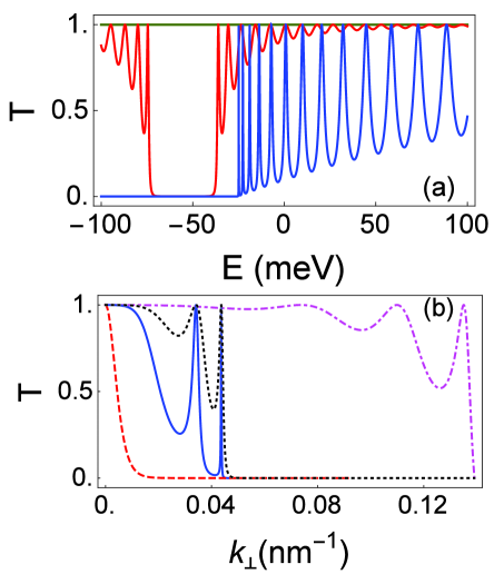
On the continuum edges where and , ideal transmissions occur at the same energies as those of the confined states on the other side of the continuum edges, i.e., , in the energy range , where confined states exist. This can be understood as coherent interferences of multiple transmissions when the incident energy resonates with the confined states at any fixed as displayed in Fig. 1.
In Fig. 2(a) we plot versus for (green), (red) and (blue). The oscillating transmission spectrum is symmetrically distributed with respect to the energy . A transmission gap between and appears corresponding to the area and in Fig. 1. For large , can be greatly reduced even when is much higher than the barrier top, or lower than the well bottom.
The dependence of on or at , , and is presented in Fig. 2(b). For , is equal to 1. The increase of greatly suppresses except for ”magic” angles, where the condition in Eq. (4) for resonance is satisfied. For valence electrons of energies less than , only those with lower than critical value can transmit across the QW. This means also that a QB is more efficient to collimate conduction electron beam along the normal line than a QW.
Based on the above momentum filtering property of WSM QWs and QBs, we can design p-n-p or n-p-n transistors made of WSM heterojunctions as collimators of electron beams. One of the prototypes can be made from two types of WSMs slabs, A and B, with well-matched lattices but different Weyl node energies. Using MBE technologies, a planar transistor can be fabricated by sandwiching a B slab of thickness in the nano scale between two A slabs. When an electron beam with electron energies near the Weyl node energy of B passes through the A-B-A nanostructure, electrons of large transverse momentums will be blocked and filtered out. The outgoing electron beam becomes then normal to the A-B interfaces. By connecting a series of parallel transistors with slightly different Weyl node energies in B, we can make collimators with wider band widths.
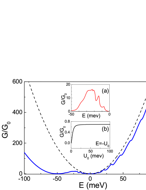
To this end, we calculate the 3D conductance with which gives the zero-temperature linear conductance of a system with cross section area over all angles at the Fermi energy equal to . is presented by the solid curve in Fig.3 with part of it zoomed in inset (a). Its counterpart of free Weyl electrons in the case of is shown by the dashed curve for the sake of comparison. In energy range where confined states exist in the QW, the conductance is only slightly lower than that without QW. It displays an oscillating behavior with the minima at corresponding to meV (=1), meV (=2), meV (=3), meV (=4), and meV (=5). In contrast, in energy range , the conductance is much smaller than that in the absence of QW and the spectrum curve becomes smooth. This conductance drop originates from the blocking of electrons with large incident angle towards the QW as explained in Fig. 1, and the transmission gap shown in Fig. 2(a). Specifically, at energy , another conductance minimum appears when only electrons propagating almost normally to the QW plane can pass across the junction with a transmission coefficient
| (5) |
The dependence of the minimal conductance on is shown in the inset of Fig. 3(b). The minimal conductance at increases with and saturates at a value about when meV. In the absence of the potential or when approaches zero, it merges with the zero conductance at the Weyl node energy .
In summary, we have shown that confined states are allowed for finite transverse wavevector in some energy range. The confined states even emerge at the edges of the continuum of free particles, and this characteristic brings about a great impact on the transmission. We find that the electronic transmission through the nanostructures is dependent on the incident angles. The Klein tunneling mechanism is generally suppressed for the obliquely incident electrons which can be confined by electrostatic potentials. However, in addition to the full transmission for normally incident electron beam, there are finite magic angles of the incidence for full transmission, which are associated to Fabry-Pérot resonances at both interfaces. Specifically, for electrons have energy equal to the QW bottom or to the QB top energy, only the normal incident electrons can pass the structure and an extra conductance minimum appears at the energy. The transmission probability through heterojunctions could be testified by the bulk resistance measurements.
Our study suggests that for p-type (n-type) Weyl materials one can apply a QW (QB) potential to make a p-n-p (n-p-n) transistor and manipulate the direction and magnitude of the charge current. When the bottom (top) energy of the QW (QB) is aligned to the Fermi energy, i.e., (), the charge current can be well collimated with the linear conductance greatly reduced by the potential. Since the energy band and electron properties are well protected by unbroken symmetry in Weyl materials, the corresponding device is expected more robust than those of normal semiconductors. In this case, n-p-n or p-n-p nanostructure transistors can be designed to collimate electron beams. Also, this transistor may be used as a tunable well for electrostatic quantum confinement, which can be deployed as a single Weyl fermion pump.
Acknowledgements.
W.-L.Y. acknowledges the helpful discussion with H. Jiang and support by the Natural Science Foundation of Jiangsu Province of China under Grant No. BK20141190 and the NSFC under Grant Nos. 11474211 and 11204197. X.-F.W. appreciates support from NSFC under Grant Nos. 11074182 and 91121021. A.M.O. kindly acknowledges support by Narodowe Centrum Nauki (NCN, National Science Center) under Project No. 2012/04/A/ST3/00331.References
- (1) M. Z. Hasan and C. L. Kane, Rev. Mod. Phys. 82, 3045 (2010).
- (2) Xiao-Liang Qi and Shou-Cheng Zhang, Rev. Mod. Phys. 83, 1057 (2011).
- (3) A. A. Burkov and L. Balents, Phys. Rev. Lett. 107, 127205 (2011); A. A. Burkov, M. D. Hook, and L. Balents, Phys. Rev. B 84, 235126 (2011).
- (4) P. Hosur and X. Qi, Comptes Rendus Physique 14, 857 (2013).
- (5) W. Witczak-Krempa, G. Chen, Y. B. Kim, and L. Balents, Annu. Rev. Condens. Matter Phys. 5, 57 (2014).
- (6) O. Vafek and A. Vishwanath, Annu. Rev. Condens. Matter Phys. 5, 83 (2014).
- (7) Q. D. Gibson, L. M. Schoop, L. Muechler, L. S. Xie, M. Hirschberger, N. P. Ong, R. Car, and R. J. Cava, Phys. Rev. B 91, 205128 (2015).
- (8) Ari M. Turner and Ashvin Vishwanath, arXiv:1301.0330.
- (9) L. Balents, Physics 4, 36 (2011).
- (10) X. Wan, A. M. Turner, A. Vishwanath, and S. Y. Savrasov, Phys. Rev. B 83, 205101 (2011).
- (11) G. Xu, H. Weng, Z. Wang, X. Dai, and Z. Fang, Phys. Rev. Lett. 107, 186806 (2011).
- (12) Y. Baum, E. Berg, S. A. Parameswaran, and Ady Stern, Phys. Rev. X 5, 041046 (2015).
- (13) Vivek Aji, Phys. Rev. B 85, 241101(R) (2012).
- (14) S. A. Parameswaran, T. Grover, D. A. Abanin, D. A. Pesin, and A. Vishwanath, Phys. Rev. X 4, 031035 (2014).
- (15) P. Hosur and Xiao-Liang Qi, Phys. Rev. B 91, 081106 (2015).
- (16) Hua Jiang, Z. Qiao, H. Liu, and Qian Niu, Phys. Rev. B 85, 045445 (2012).
- (17) S. A. Skirlo, L. Lu, Y. Igarashi, J. Joannopoulos, and M. Soljacic, Phys. Rev. Lett. 115, 253901 (2015).
- (18) Q.-D. Jiang, H. Jiang, H. Liu, Q.-F. Sun, and X. C. Xie, Phys. Rev. Lett. 115, 156602 (2015).
- (19) S. A. Yang, H. Pan, and F. Zhang, Phys. Rev. Lett. 115, 156603 (2015).
- (20) K.-Y. Yang, Y.-M. Lu, and Y. Ran, Phys. Rev. B 84, 075129 (2011).
- (21) Teemu Ojanen, Phys. Rev. B 87, 245112 (2013).
- (22) J. Liu and D. Vanderbilt, Phys. Rev. B 90, 155316 (2014).
- (23) H. Weng, C. Fang, Z. Fang, B. A. Bernevig, and Xi Dai, Phys. Rev. X 5, 011029 (2015).
- (24) S.-Y. Xu, I. Belopolski, C.-C. Lee, G. Chang, B. Wang, N. Alidoust, G. Bian, M. Neupane, C. Zhang, S. Jia, A. Bansil, H. Lin, and M. Zahid Hasan, Nature Commun. 6, 7373 (2015).
- (25) C. Shekhar, F. Arnold, S.-C. Wu, Y. Sun, M. Schmidt, N. Kumar, A. G. Grushin, J. H. Bardarson, R. Donizeth dos Reis, M. Naumann, M. Baenitz, H. Borrmann, M. Nicklas, E. Hassinger, C. Felser, and B. Yan, arXiv:1506.06577.
- (26) B. Q. Lv, H. M. Weng, B. B. Fu, X. P. Wang, H. Miao, J. Ma, P. Richard, X. C. Huang, L. X. Zhao, G. F. Chen, Z. Fang, X. Dai, T. Qian, and H. Ding, Phys. Rev. X 5, 031013 (2015); A. Vishwanath, Physics 8, 84 (2015).
- (27) C. Zhang, S.-Y. Xu, I. Belopolski, Z.n Yuan, Z. Lin, B. Tong, N. Alidoust, C.-C. Lee, S.-M. Huang, H. Lin, M. Neupane, D. S. Sanchez, H. Zheng, G. Bian, J. Wang, C. Zhang, T. Neupert, M. Zahid Hasan, S. Jia, arXiv:1503.02630.
- (28) C. Shekhar, A. K. Nayak, Y. Sun, M. Schmidt, M. Nicklas, I. Leermakers, U. Zeitler, Z. Liu, Y. Chen, W. Schnelle, J. Grin, C. Felser, and B, Yan, Nature Phys. 11, 645 (2015).
- (29) Z. K. Liu, B. Zhou, Y. Zhang, Z. J. Wang, H. M. Weng, D. Prabhakaran, S.-K. Mo, Z. X. Shen, Z. Fang, X. Dai, Z. Hussain, and Y. L. Chen, Science 343, 864 (2014).
- (30) S.-Y. Xu, C. Liu, S. K. Kushwaha, R. Sankar, J. W. Krizan, I. Belopolski, M. Neupane, G. Bian, N. Alidoust, T.-R. Chang, H.-T. Jeng, C.-Yi Huang, W.-F. Tsai, H. Lin, P. P. Shibayev, F.-C. Chou, R. J. Cava, and M. Zahid Hasan, Science 347, 294 (2015).
- (31) Z. K. Liu, J. Jiang, B. Zhou, Z. J. Wang, Y. Zhang, H. M. Weng, D. Prabhakaran, S-K. Mo, H. Peng, P. Dudin, T. Kim, M. Hoesch, Z. Fang, X. Dai, Z. X. Shen, D. L. Feng, Z. Hussain, and Y. L. Chen, Nature Mater. 13, 677 (2014).
- (32) Z. Wang, H. Weng, Q. Wu, X. Dai, and Z. Fang, Phys. Rev. B 88, 125427 (2013).
- (33) T. Liang, Q. Gibson, M. N. Ali, M. Liu, R. J. Cava, and N. P. Ong, Nat. Mater. 14, 280 (2015).
- (34) Y. Liu, C. Zhang, X. Yuan, Tang Lei, C. Wang, L. He, R. Che, and F. Xiu, NPG Asia Materials 7, e221 (2015).
- (35) Z.-G. Chen, C. Zhang, Y. Zou, E. Zhang, L. Yang, F. Xiu, and J. Zou, Nano Lett. 15, 5830 (2015).
- (36) C.-Z. Li, L.-X. Wang, H. Liu, J. Wang, Z.-M. Liao, and D.-P. Yu, Nat. Commun. 6, 10137 (2015) .
- (37) H. B. Nielsen and M. Ninomiya, Phys. Lett. B 130, 389 (1983).
- (38) X. Huang, L. Zhao, Y. Long, P. Wang, D. Chen, Z. Yang, H. Liang, M. Xue, H. Weng, Z. Fang, X. Dai, and G. Chen, Phys. Rev. X 5, 031023 (2015).
- (39) X. Yang, Y. Liu, Z. Wang, Y. Zheng, and Z.-A. Xu, arXiv:1506.03190.
- (40) J. M. Pereira, V. Mlinar, F. M. Peeters, and P. Vasilopoulos, Phys. Rev. B 74, 045424 (2006).
- (41) M. Barbier, F. M. Peeters, P. Vasilopoulos, and J. M. Pereira, Phys. Rev. B 77, 115446 (2008); M. Barbier, P. Vasilopoulos, F. M. Peeters, and J. M. Pereira, ibid. 79, 155402 (2009).