Single electron gating of topological insulators
Abstract
Introducing, observing, and manipulating individual impurities coupled to a host material offers the opportunity to create new device concepts based on single spin and charge states. Because of potential applications in spintronics and magneto-electrics, such an approach would be particularly useful for topological insulators (TI), a recently discovered material class hosting spin-momentum-locked surface states. To make them useful for new technologies, a robust control of their interaction with external perturbations is required. However, traditional approaches such as metal electrodes or doping proved to be problematic and resulted in strong mesoscopic fluctuations making the spin-momentum locking ill-defined. Here, we demonstrate the effective gating of TIs by coupling molecules to their surface which, by using electric fields, allow to dynamically control the interface charge state by adding or removing single electrons. This process creates a robust transconductance bistability resembling a single-electron transistor. Our findings make hybrid molecule/TI interfaces functional elements while at the same time pushing miniaturization at its ultimate limit. This opens a new avenue for all electric-controlled spintronic devices based on these fascinating materials.
In the semiconductor industry, the presence of impurities is traditionally considered a limiting factor degrading device performance through the creation of disorder, especially given the ongoing trend towards device miniaturization RA2005 . Recently, the effects of single dopants were observed in commercial devices PWJ2010 , severely constraining reproducibility. However, the dramatically improved control of matter at the nanoscale also provided the idea to address single impurities individually SOK2005 ; KF2011 . Within this framework, impurities are no longer considered a problem but as an opportunity to push miniaturization to its ultimate level while at the same time creating plenty of room to realize new device concepts, such as single-dopant transistors FMM2011 or single-spin solid-state quantum computers ABD2013 .
In this context, the recently discovered topological insulators (TI) represent a promising new class of materials. TIs are insulating in the bulk but conductive on their surface, where they host linearly dispersing Dirac fermions protected by time-reversal symmetry KWB2007 ; HQW2008 . Strong spin-orbit coupling perpendicularly locks the spin to the momentum, resulting in a chiral spin texture which forbids backscattering RSP2009 . All these properties make TIs highly attractive for spintronics, magneto-electrics, and quantum computing PM2012 . Up to now, however, the controlled gating of topological states, which is required to tune both the spin-texture and the conductance, has proved problematic Y2013 . In particular, interfacing TIs with external perturbations using traditional approaches such as metal electrodes or dopants resulted in the undesired creation of strong mesoscopic fluctuations which make the spin-momentum locking ill-defined over length scales of few nanometers BRS2011 ; SRB2014 .
More recently, it has been demonstrated that all these limitations can be overcome at once by using molecules as building blocks SBK2014 ; SZY2014 ; BSK2015 ; JNS2015 ; YCL2015 ; CPL2016 . Molecules have already been successfully used in the past to create hybrid heterostructures with functionalities going beyond those of their constituents RGB2005 ; CHW2009 . Especially phthalocyanines (Pc) have been recently reported to host several unconventional properties FSP2011 ; MRC2012 ; WHP2015 . In this case, self-assembly processes driven by inherent interactions have been identified as a versatile way to engineer highly homogeneous potential landscapes interfaced with topological states.
Here, we demonstrate that the charge state of molecules coupled to TIs can be dynamically switched by using local electric fields. This leads to a transconductance bistability which can be effectively described by a double barrier quantum capacitance (DBQC) effect L1988 . By spatially mapping the response of the hybrid molecule/TI interface to the charging/discharging process as a function of the applied voltage, a strongly conducting ring of progressively larger diameter develops around each molecule once the ionization threshold is reached, signaling the presence of strong Coulomb repulsions which are only weakly screened by the 2D topological electron gas. Overall, this process results in the gating of the topological insulator surface, which can thus be reproducibly controlled and closely resembles the voltage-current characteristic of a single-electron transistor (SET) device K1992 .
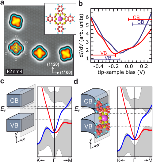
Figure 1a shows a dilute concentration of MnPc molecules coupled to the Bi2Te3 surface. All molecules are adsorbed with the same geometry, i.e. with the central Mn atom sitting on top of a Te atom, as represented by grey circles interpolating the Te surface lattice to the molecule position. As described in detail in Ref. 14, three different molecular orientations are visible, which result from the combined symmetry of the molecules (4-fold) with that of the surface (6-fold). Comparison of the Bi2Te3 local density of states as inferred by scanning tunneling spectroscopy (STS) before (blue curve in Fig. 1b) and after deposition (red) allows to map the evolution of the electronic properties at the hybrid molecule/TI interface. Subsequent to molecule deposition a moderate negative energy shift is visible, signaling the creation of an interface dipole which bends the Bi2Te3 surface electronic bands, as illustrated in Fig. 1c,d. This observation demonstrates that molecules act as a static potential effectively gating the surface of topological insulators. As described in the following, this has far reaching implications as their charge state can dynamically be controlled by local electric fields.
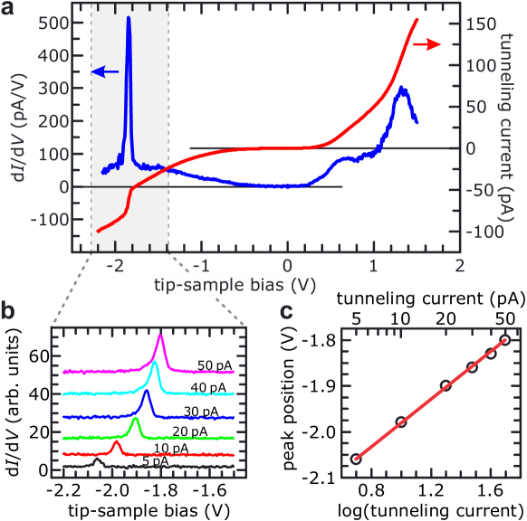
Figure 2a reports the curve (red line) and the differential conductance (blue) obtained by positioning the tip over the Pc’s central Mn atom. A broad shoulder with onset at V and a peak centered at V are visible in the signal which correspond to a hybrid interface resonance state (IS) and a Mn state of character, respectively SBK2014 (see Supplementary Information). In addition, an intensive and very sharp peak shows up at negative bias which does not correspond to any conventional electronic state feature. With the set-point current chosen in Fig. 2a, i.e. pA, it appears at approximately V. As signaled by a step-like feature in the curve, its onset is accompanied by a sudden increase of the tunneling current, suggesting that the molecule/TI interface switches to a different state.
Figure 2b reveals that the position of this sharp and intensive peak strongly depends on the tip–sample distance which can conveniently and precisely be controlled by the STM set-point current. In addition, due to the stronger overlap between the tip’s and sample’s wave functions the peak height gradually rises. Fig. 2c report the energy positions of the peaks visible in b as a function of the tunneling current flowing through the molecule–TI junction. Since the tunneling current exponentially depends on the barrier width, the linear dependence visible in the semi-logarithmic plot demonstrates that the change in the transconductance is inversely proportional to the the tip-sample separation.
Within a single impurity picture, these observations can be effectively explained as an electric field–driven reversible ionization process, similar to earlier findings around dopants buried into conventional semiconductors TVL2008 ; LG2010 or molecules coupled to insulating substrates WZC2004 ; WHP2015 . However, TIs are fundamentally different with respect to these systems since they host on the surface a 2D electron gas which is generally expected to effectively screen electric fields. Our measurements, in line with previous observations on the surface energy level alignment CSZ2010 and the charge states of bulk dopants SJW2012 , clearly demonstrates this not being the case. Indeed, as schematically illustrated in Fig. 3a, the electric field partially penetrates into the TI, bending its band structure creating a quantum well at the surface (see Supplementary Information). Note that the weak screening of topological states as revealed in our experiments has far reaching implications. It proves that topological states do not behave as a simple metal and imply the existence of an upper limit to their transport properties.
The creation of hybrid molecule-TI interfaces has several advantages, namely: (i) the high degree of charge localization of molecules results in an electronic occupation which can change only by integer numbers, creating a well-defined sequence of discrete states generated by strong Coulomb repulsions, (ii) molecules can be placed onto TI surfaces without perturbing their topological states by scattering SBK2014 , (iii) contrary to conventional doping, their hybridization with the host is reduced, thus preserving their functionality and (iv) their distribution can be precisely controlled through self-assembly processes BSK2015 .
Fig. 3b-d displays a more detailed picture how the band diagram of the tip–molecule–TI tunnel junction changes upon application of a negative bias voltage and how this results in an electric field–driven molecular ionization process which eventually acts back on the TI by gating the topological surface state. At zero bias (Fig. 3b) the Fermi levels of tip and sample are aligned. The valence and conduction band edges of the TI are only moderately shifted downwards due to the above-mentioned interface dipole associated to molecule adsorption (cf. Fig. 1d). The hybrid interface resonance state (IS) is energetically located at about eV, i.e. in the empty states. As a small negative tip–sample bias voltage is applied (Fig. 3c) the electric field partially penetrates into the TI surface and further bends its valence and conduction band edges down. Electrostatically, this is equivalent to two capacitors connected in series: within this picture one capacitor would represent the tip and the 2D topological electron gas on either side of the vacuum barrier, the other one the quantum well at the TI surface. The voltage partition across the tip–molecule–TI junction is simply defined by the ratio of the respective capacitances (see Supplementary Information). Since the IS is locked to the TI band structure it also shifts downwards, but it still remains above the Fermi level of the TI.
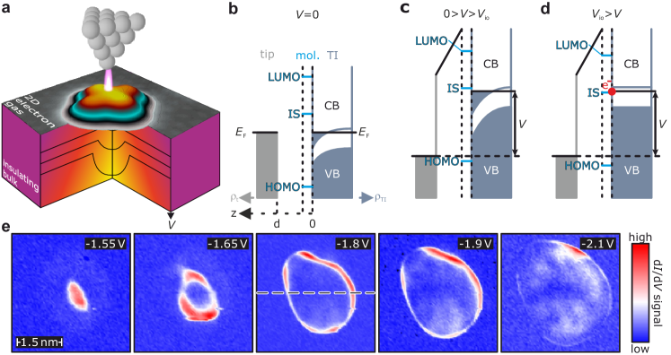
At a certain threshold voltage the band bending is so strong that the IS crosses the Fermi level of the TI and occupation becomes energetically favorable. This situation is sketched in Fig. 3d. The additional electron at the interface creates a repulsive potential which pushes up the surface band structure acting against the band bending (see below). This increases the density of states available for electron tunneling at the surface, an effect considered to be particularly important in situations when the tip is away from the molecule and direct tunneling through the conduction channel involving the IS becomes insignificant. Overall, these effects result in the observed step-like increase of the current-voltage relation (cf. Fig. 2a) which creates a bistability that can be robustly controlled.
Interestingly, we found that when the tip is displaced laterally from the central Mn atom, its electric field can still effectively gate the surface and ionize the molecule. Fig. 3e shows a bias voltage–dependent series of maps measured at constant tip–sample separation over the same molecule. The position where the respective threshold bias is reached is signaled by a high signal. While this threshold bias amounts to about V at the central position of the molecule,sharp rings with increasing diameters can be observed at more negative bias. Note, that the ring diameter eventually exceeds the size of the molecule. Obviously, the additional, highly localized charge that results from the molecule ionization process cannot be effectively screened by the topological states. As a result the TI is gated, making such an approach a suitable way to manipulate macroscopic transport properties.
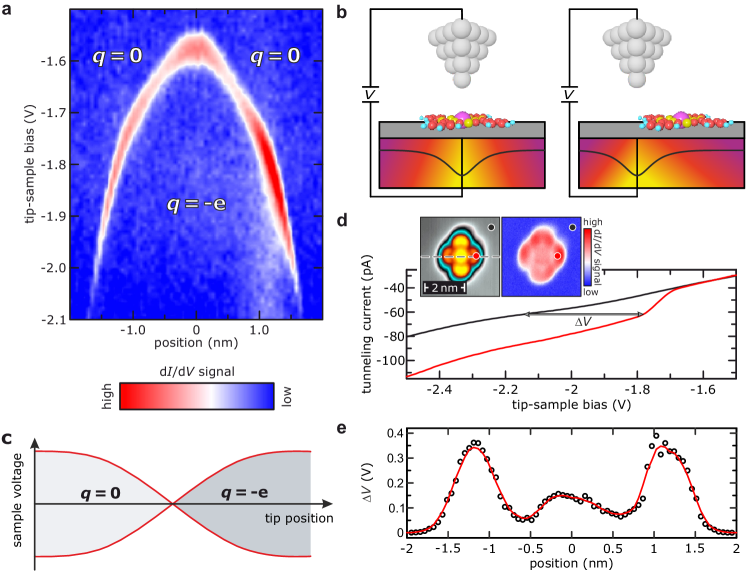
Fig. 4a summarizes the sequence of spectra taken along the molecule axis indicated in the central panel of Fig. 3e. By moving towards the edge of the molecule the ionization threshold increases as a direct consequence of the reduced tip-induced gating illustrated in Fig. 4b but always takes place in a voltage range between V. Although the ionization voltage somewhat depends on the exact tip shape (note the slightly different thresholds obtained using different tips but same stabilization parameters in Fig. 2 and 4), our data indicate that this general trend is very robust, with all molecules displaying the very same behavior (see Supplementary Information) compatible with low voltage electronic devices.
Overall, the voltage-current relation resembles the transport characteristic of a SET K1992 , where a gate voltage allows to select the discrete number of occupied states determining the current flowing between two terminals, i.e. source and drain, once a voltage is applied. In the present case, the bias applied through the tunneling junction correspond to , while the tip position mimics a gate potential which allows—through capacitive coupling—to regulate the voltage drop at the molecule/TI interface FKS2012 ; ZWB2014 . The discrete characteristic is schematically illustrated in Fig. 4c, where differently shaded areas correspond to distinct transconductance states that are separated by Coulomb blockade.
In order to quantify the extension and the strength of the gating potential created by the additional electron—both important quantities which directly impact macroscopic properties like transport—we further analyzed the steps visible in the tunneling current at the ionization threshold. Fig. 4d shows tunneling spectra measured above a molecule ligand and on the bare TI surface (see red and black points in the topographic image in the left inset of Fig. 4d, respectively). While the spectra overlap at low negative bias voltage ( V), they are shifted by a fixed voltage beyond the ionization threshold, where a sudden step-like increase of the current is visible.
The subtle changes induced in the tunneling process by the molecule’s ionization prevent an exact quantification of the its gating potential. Nevertheless, similar to previous observation on single dopants buried in conventional semiconductors TVL2008 , an estimation of the gating potential can be obtained by analyzing the voltage shift between the ionized and neutral curves at a position corresponding to the step-like increase of the tunneling current ( pA in this case). Results obtained along the line in the left inset of Fig. 4d are reported in Fig. 4e. Values up to V are observed at a distance of about 1 nm from the center of the molecule. This value is close to the sum of the static band bending induced by the molecule adsorption process, i.e. 70 meV, plus the 300 meV shift required to align the interface state with the Fermi level, and therefore consistent with the flat band condition sketched in Fig. 3d.
Our findings illuminate the interaction of topological states with the localized Coulomb potential of single electron charges. The use of the high degree of charge localization achievable in molecules opens up a new pathway for reliably interfacing TIs with well-defined external perturbations. If correlated with the ionization state of particular chemical species like in the present case, the resulting bistability proves that hybrid molecule/TI interfaces may be suitable as sensors. More generally, the capability to dynamically gate molecules to the single-electron level through electric fields, paves the way towards purely electrically controlled spintronic devices, thereby bringing us a significant step closer towards an application of this fascinating class of materials.
The authors gratefully acknowledge discussions with Michael Flatté.
Methods Experiments have been performed in an STM operated at K. n-doped Bi2Te3 single-crystals were grown using the Bridgman technique. The crystal structure consists of alternating planes of Bi and Te up to the formation of a quintuple layer with the sequence Te-Bi-Te-Bi-Te. Quintuple layers are weakly coupled by van der Waals forces thus offering a natural cleaving plane. The Bi2Te3 single crystals have been cleaved in UHV at a base pressure of mbar and immediately inserted into the STM. Because of the above mentioned crystal structure, cleaved crystals are always Te terminated. MnPc molecules (Sigma-Aldrich) were deposited directly onto the cold Bi2Te3 surface by using a home-made Knusden cell and annealed at room temperature. STM measurements have been performed using electrochemically etched tungsten tips. Spectroscopic data have been acquired by lock-in technique ( Hz, = 10 mV).
References
- (1) S. Roy, & A. Asenov, Where Do the Dopants Go? Science 309, 388-390 (2005).
- (2) M. Pierre et al., Single-donor ionization energies in a nanoscale CMOS channel. Nature Nanotechnology 5, 133-137 (2010).
- (3) T. Shinada, S. Okamoto, T. Kobayashi, I. Ohdomari, Enhancing semiconductor device performance using ordered dopant arrays. Nature 437, 1128-1131 (2005).
- (4) P. M. Koenraad, M. E. Flatté, Single dopants in semiconductors. Nature Materials 10, 91-100 (2011).
- (5) M. Fuechsle et al., A single-atom transistor. Nature Nanotechnology 7, 242-246 (2012).
- (6) D. D. Awschalom, L. C. Bassett, A. S. Dzurak, E. L. Hu, J. R. Petta, Quantum Spintronics: Engineering and Manipulating Atom-Like Spins in Semiconductors. Science 339, 1174-1179 (2013).
- (7) M. König, et al., Quantum Spin Hall Insulator State in HgTe Quantum Wells Science 318, 766-770 (2007).
- (8) D. Hsieh, et al. A topological Dirac insulator in a quantum spin Hall phase. Nature 452, 970-974 (2008).
- (9) P. Roushan, et al., Topological surface states protected from backscattering by chiral spin texture. Nature 460, 1106-1109 (2009).
- (10) D. Pesin, A. H. MacDonald, Spintronics and pseudospintronics in graphene and topological insulators. Nature Materials 11, 409-416 (2012).
- (11) W.-M. Yang, C.-J. Lin, J. Liao, Y.-Q. Li, Electrostatic field effects on three-dimensional topological insulators. Chinese Phys. B 22, 097202 (2013).
- (12) H. Beidenkopf, et al., Spatial fluctuations of helical Dirac fermions on the surface of topological insulators. Nature Physics 7, 939-943 (2011).
- (13) P. Sessi, et al., Signatures of Dirac fermion-mediated magnetic order. Nature Communications 5, 5349 (2014).
- (14) P. Sessi, et al., Probing the Electronic Properties of Individual MnPc Molecules Coupled to Topological States. Nano Lett. 14, 5092-5096 (2014).
- (15) Y. R. Song, et al. , Magnetic anisotropy of van der Waals absorbed iron(II) phthalocyanine layer on Bi2Te3. Phys. Rev. B 90, 180408 (2014).
- (16) T. Bathon, et al., Systematics of molecular self-assembled networks at topological insulators surfaces. Nano Lett. 15, 2442 (2015).
- (17) S. Jakobs, et al., Controlling the Spin Texture of Topological Insulators by Rational Design of Organic Molecules. Nano Lett. 15, 6022 (2015).
- (18) H.-H Yang, et al., Organic Monolayer Protected Topological Surface State Nano Lett. 15, 6896 (2015).
- (19) M. Caputo, et al., Manipulating the topological interface by molecular adsorbates: Adsorption of Co-Phthalocyanine on Bi2Te3. Nano Lett. DOI: 10.1021/acs.nanolett.5b02635 (2016).
- (20) A. R. Rocha, et al., Towards molecular spintronics. Nature Materials 4, 335-339 (2005).
- (21) M. Cinchetti, et al., Determination of spin injection and transport in a ferromagnet/organic semiconductor heterojunction by two-photon photoemission. Nature Materials 8, 115-119 (2009).
- (22) K. J. Franke, G. Schulze, J. I. Pascual, Competition of superconducting phenomena and Kondo screening at the nanoscale. Science 332, 940-944 (2011).
- (23) A. Mugarza, R. Robles, C. Krull, R. Korytár, N. Lorente, & P. Gambardella, Electronic and magnetic properties of molecule-metal interfaces: Transition-metal phthalocyanines adsorbed on Ag(100) Phys. Rev. B 85, 155437 (2012).
- (24) B. Warner, et al., Tunable magnetoresistance in an asymmetrically coupled single-molecule junction. Nature Nanotechnology 10, 259-263 (2015).
- (25) S. Luryi, Quantum capacitance devices. Appl. Phys. Lett. 52, 501-503 (1998).
- (26) M. A. Kastner, The single-electron transistor. Rev. Mod. Phys. 64, 849 858 (1992).
- (27) K. Teichmann, et al. Controlled charge switching on a single-donor with a scanning tunneling microscope. Phys. Rev. Lett. 101, 076103 (2008).
- (28) D. H.Lee, J. A. Gupta, Tunable field control over the binding energy of single dopants by a charged vacancy in GaAs. Science 330, 1807-1810 (2010).
- (29) Wu, S. W., Nazin, G.V., Chen, X., Qiu, X. H. & Ho. W. Control of relative tunneling rates in single molecule bipolar electron transport. Phys. Rev. Lett. 93, 236802 (2004).
- (30) P. Cheng, et al., Landau Quantization of Topological Surface States in Bi2Se3. Phys. Rev. Lett 105, 076801 (2010).
- (31) C.-L. Song, et al., Gating the charge state of single Fe dopants in the topological insulator Bi2Se3 with a scanning tunneling microscope. Phys. Rev. B 86, 045441 (2012).
- (32) I. Fernandez-Torrente, et al., Gating the Charge State of Single Molecules by Local Electric Fields Phys. Rev. Lett 108, 036801 (2012).
- (33) H. Zheng, A. Weismann, & R. Berndt, Tuning the electron transport at single donors in zinc oxide with a scanning tunnelling microscope. Nature Communications 5, 2992 (2014).