Multi-Valued Routing Tracks for FPGAs in 28nm FDSOI Technology
Abstract
In this paper we present quaternary and ternary routing tracks for FPGAs, and their implementation in 28nm FDSOI technology. We discuss the transistor level design of multi-valued repeaters, multiplexers and translators, and specific features of FDSOI technology which make it possible. Next we compare the multi-valued routing architectures with equivalent single driver two-valued routing architectures. We show that for long tracks, it is possible to achieve upto 3x reduction in dynamic switching energy, upto 2x reduction in routing wire area and 10% reduction in area dedicated to routing resources. The multi-valued tracks are slightly more susceptible to process variation. We present a layout method for multivalued standard cells and determine the layout overhead.We conclude with various usage scenarios of these tracks.
I Introduction
Multi-valued signalling has always been used in communication, mainly to increase data rate. e.g Techniques such as M-ary PAM (Pulse amplitude modulation) are used in the Ethernet protocol. So far, on-chip communication restricts itself to binary signalling, because the receiver and transmitter complexity often outweighs the potential benefits of multi-valued signalling. But as chips are growing bigger, and since the interconnect resistance does not scale with technology [17], interconnect (RC) delay plays an ever more important role in chip design. Interconnect capacitance also increases from generation to generation as lines are more closely spaced. To compensate for RC delays, more buffers need to be inserted, giving rise to higher interconnect power consumption. For this reasons alternative interconnect technologies such as optical, transmission lines etc. have been proposed. [17, 12]
In this article we focus on multi-valued communication within the chip to alleviate some of the problems related to interconnects. More specifically we concentrate on routing tracks in FPGAs. Routing resources take up the most of the area in an FPGA [1], and also account for 60-70 % of power consumption [22]. Thus power efficiency of routing resources, and decrease in routing congestion are always welcome.
Numerous researchers have proposed ternary and quaternary logic designs over the years [24, 11, 7]. A majority of these designs use transistors with several different s (Threshold Voltage) which require different amount of channel dopings and thus leading to complex processes. Some recent implementation of MVL arithmetic circuits can be found in [23]. [9] proposes ternary signalling for asynchronous logic. [5, 14] proposes MVL lookup Table architectures. [13] proposes ternary logic devices based on Si-Ge Diodes. One of the successful commercialization of MVL is the strataflash from Intel [8, 4].
In this article we discuss the use of multi-valued logic for on-chip communications in FPGAs. To implement these circuits we use an interesting feature of the contemporary FDSOI (Fully Depleted Silicon On Insulator) technology, namely its capability to fine-tune the by varying the Body-Bias.
I-A Organisation
The rest of the article is organised in the following fashion. In section II we provide a brief update on the FDSOI technology, and discuss the back-biasing technique in detail. In section III we present the multi-valued logic systems and evaluate the dynamic switching energies. In section IV we present the various primitives such as repeaters, multiplexers and their operation. In section V we present the experimental architectures and experimental methods to evaluate the performance of multi-valued tracks. In section VI we present the experimental results and in section VII we discuss the variability and reliability issues. In section VIII we present an outline of the method used to layout these circuits and we calculate the layout overhead. We conclude with various usage scenarios of these routing tracks.
II Brief Overview of FDSOI Technology
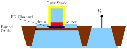
Figure 1 depicts the structure of a FDSOI transistor. The main difference with the bulk CMOS is the buried oxide (BOx) which insulates the well from the channel. The silicon layer/channel is fully depleted, that is, it does not contain any active charge carriers. Some of the potential benefits of this structure are
-
•
Improved Junction capacitance. Lower parasitic capacitance, i.e lower source-drain capacitance thanks to dielectric isolation.
-
•
Better Electro-static control of the channel, which results in a near ideal sub-threshold slope of 60mv/decade [26], and reduced DIBL (Drain induced Barrier Lowering)
-
•
Improved variation as the channel is not doped. One of the major causes of variation is RDF (Random Dopant Fluctuation). Thus variability coefficient for transistors with same size is 2-3 times less for FDSOI [3]
-
•
The transistor is controlled through two independent gates. The can be modulated by applying back-bias to the back plane (BP).
In FDSOI the can be controlled through three different methods
-
•
By doping the substrate below the Buried Oxide (BOx), also known as back plane (BP). When the BP is of opposite polarity to source/drain the increases. It is know as the RVT (Regular ) flavor. When the BP is of same polarity as source/drain, we get the LVT (Low ) flavor and it has a lower .
-
•
The can be controlled by applying a voltage to the backplane, however to avoid formation of forward biased diodes in the substrate there are some limitations. Figure: 1(b) shows the back biasing characteristics. The is lowered during Forward Body Bias (FBB) corresponding to for PMOS and for NMOS. Similarly can be augmented using Reverse Body Bias (RBB).
RVT RBB upto -3V FBB upto +300mv LVT FBB upto +3V RBB upto -300mv -
•
It is also possible to increase by increasing the gate length. This is known as poly-biasing.
In this article we will use a combination of the above three methods to implement multi-valued logic. For more details about UTBB-FDSOI please refer to [16].
III Multi-Valued Logic Systems (MVL)
While ternary systems are the optimum [2], there are many advantages of implementing arithmetic circuits in a multi valued logic systems [24]. In this article we consider mainly quaternary systems, but the circuits presented can be easily adapted to ternary systems.
On top of arithmetic advantages, there are some physical advantages related to these systems, particularly when used to communicate over a long distance. They are namely dynamic switch energy and routing congestion.
-
•
The dynamic switching energy in the context of on-chip communication for quaternary logic is detailed in table I. We can see that average energy /transition for quaternary is . Similarly it can be shown that average energy /transition for ternary systems is .
-
•
For quaternary logic a reduction of 50% in routing wire area is achievable. For ternary logic systems upto 33% reduction in routing wire area can be achieved. This calculation is based on the fact that 2 ternary wires can transmit as much information as 3 binary wires.
| 4-Valued transitions | |
|---|---|
| Transitions | Energy |
| ,,, | 0 |
| Av. Energy/Tran | |
| 2-Valued transitions | |
|---|---|
| transitions | Energy |
| , | 0 |
| Av. Energy/Tran | |
IV Primitives for Multi-Valued Routing
IV-A Down-Literal Converters
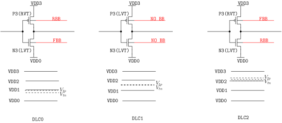
| Down-Literal Converters | |||
| input | DLC0 | DLC1 | DLC2 |
| 0 | 3 | 3 | 3 |
| 1 | 0 | 3 | 3 |
| 2 | 0 | 0 | 3 |
| 3 | 0 | 0 | 0 |
Down literal converters (DLCs) are the basic primitives of MVL implementation with binary CMOS logic [24]. They help in categorizing the multiple valued signals in different bins. Table 2 describes the three down literal converters associated with Quaternary logic. DLC0 distinguishes between logic level and . DLC1 distinguishes between and and so on. In figure 2 we can see implementation of DLCs in FDSOI technology with the use of back biasing. For DLC0 the threshold voltage is increased by using a RVT PMOS transistor and Reverse Back-biasing, and is engineered to be between logic level 0 and 1. In the same fashion other DLCs are implemented. It is also possible to use poly-biasing (see sec. II) to increase the reverse bias.
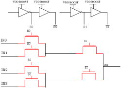
IV-B Multi-Valued Multiplexers
The multiplexer described in figure 3 assumes that inputs and outputs are multi-valued, whereas the select input is binary. In this case we assume that the configuration memory points are actually 6T binary SRAM cells.
The use of boosted gate voltages is commonplace to avoid any signal degradation for logic level ’1’. The same gate-boosted transistor can also pass all the levels in a multiple valued logic. It is also possible to use transmission gates instead, but we consider pass transistors as they have lower transistor count.
IV-C Multi-Valued Repeater Circuits
IV-C1 Operation
| IN | N0 | P0 | N1 | P1 | N2 | P2 | N3 | P3 | N4 | P4 | N5 | P5 |
| 0 | OFF | ON | OFF | ON | ON | OFF | OFF | ON | ON | OFF | ON | OFF |
| 1 | OFF | ON | ON | OFF | OFF | ON | OFF | ON | ON | OFF | ON | OFF |
| 2 | ON | OFF | ON | OFF | OFF | ON | OFF | ON | ON | OFF | OFF | ON |
| 3 | ON | OFF | ON | OFF | OFF | ON | ON | OFF | OFF | ON | OFF | ON |
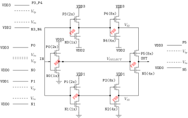
Figure 4 depicts the circuit diagram for the quaternary repeater circuit consisting of 12 transistors. The engineered Vths of each transistor pair are indicated in the diagram. The transistors selects among the level and . When the input belongs to the transistor is on and net is connected to the output. When the input belongs to the transistor is on and net is connected to the output. The transistors , act as a buffer for the levels and the transistors , act as a buffer for the levels.
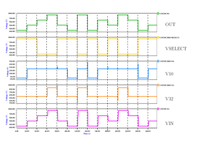
The states of each transistor for various levels at the input are described in table III. Detailed operation of the quaternary repeater can be understood from the waveforms of its internal nodes presented in figure 5.
The ratio of average dynamic switching energy of such a repeater w.r.t 2 binary tracks can expressed as:
| (1) |
Where is the input capacitance of the transistor pairs at the input of the repeater. The input capacitance of a quaternary repeater is three times that of a binary buffer. For this reason with short track lengths where the energy consumption and delay are much higher. As the track length grows the ratio of dynamic energy approaches .
This gain in energy comes with an associated increase in delay.
Here we present a simplified analysis of the repeater delay. In our simplified model, the resistance and the capacitance of an interconnect line are replaced by a effective capacitance () driven by the gate [20]. is a function of the interconnect R&C. We assume charging of this effective capacitance by a current source (i.e MOS). Although this is an approximate model it is adequate to explain the design trade-offs.
In general, with above assumptions, given the same transistor dimensions, and the same input slew rate, the delay (high to low) is proportional to where is between 1 and 2 for newer technologies due to velocity saturation [21], and is the NMOS threshold voltage.
The ratio of delay can be thus expressed as
| (2) |
Note that we have considered the worst case delay in the quaternary case, i.e transitions where the voltage swing is lowest .
For long wires where we can simplify the above to
| (3) |
In the quaternary repeater we have forward biased the driving stage transistors lowering their Vth. So we need to slightly modify the above equation, where denotes the modified for NMOS transistor.
| (4) |
In case we forward bias the driving transistors such that we can expect around 80% increase in delay. However there will be a considerable increase in leakage power ( 4x) as can be seen from fig. 6 (assuming to be equal to ).
Figure 6 plots the energy and delay comparison of the quaternary and binary repeaters. We have optimized the 4-valued repeater circuits by varying the back-biasing with various different goals, namely FAST is optimized for delay, and LL is optimized for low leakage.
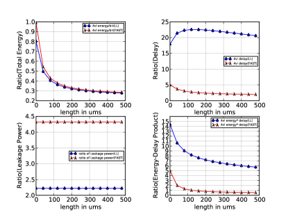
The energy delay plots of these repeaters with varying routing track length is shown in figure 6. They plot the ratio of energy and delay for multi-valued repeaters w.r.t equivalent configurations with binary buffers. For quaternary, one 4-valued wire is compared with 2 binary wires, transmitting the same information. In the binary case we use a tapered 2 stage binary buffer with the 1x transistors for input stage, and 4x transistor for output stage. The tracks are terminated with standard four inverter loads. We simulated a single repeater driving a track of varying length, with a test vector where all transitions (as shown in table. I) are equally represented.
The test-vectors use a cycle time of 10ns (100MHz) for FAST and 70ns(15 MHZ) for LL. This information is used to separate the leakage power from the dynamic power. The plotted values are ratios of equivalent quantities w.r.t the value measured in the base architecture.
We have also plotted the energy delay product with varying length of tracks, and we see indeed at longer track lengths multi-valued signalling gets interesting. Please note, that these calculations are done at 100MHz (15MHz for LL) , so the effect of leakage is mitigated. For low operating frequencies( KHz) the energy delay product will be largely dominated by leakage power.
IV-D Multi-Valued to Binary Translator Circuits

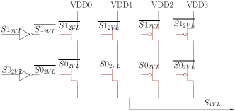
The multi-valued routing tracks can be used in the context of a end-to-end multi-valued FPGA, or it can also be used in a binary FPGA to implement bus-based tracks [28]. In the later scenario we will need binary to quaternary translators and their counterparts. In fig. 7 we present the binary/Quaternary translators. The design can be extended to include ternary translators as well.
In Fig. 7(a) we use DLCs to convert a quaternary signal to two binary signals. The output of the DLC1 is used to control the multiplexer and the signal levels are detailed in table IV.
| DLC0 | DLC1 | DLC2 | SELECT | S0 | S1 | |
| VDD0 | VDD3 | VDD3 | VDD3 | 1(VDD3) | 1(VDD3) | 1(VDD3) |
| VDD1 | VDD0 | VDD3 | VDD3 | 1(VDD3) | 0(VDD0) | 1(VDD3) |
| VDD2 | VDD0 | VDD0 | VDD3 | 0(VDD0) | 1(VDD3) | 0(VDD0) |
| VDD3 | VDD0 | VDD0 | VDD0 | 0(VDD0) | 0(VDD0) | 0(VDD0) |
Fig. 7 depicts the binary-to-quaternary translator. The quaternary levels (i.e VDD0,VDD1,VDD2,VDD3) are routed to the output depending on the input binary values (). We can see from the diagram that only one of the paths can be activated at one time.
V Design of Experiment
In this section we present the experiments to compare power consumption and delay of Multi-Valued FPGA architectures and the base architecture, which is a binary mesh FPGA with single-driver tracks [15]. Single driver tracks are most common in modern FPGAs due to their reduced capacitative loads and better area-delay performance.
V-A Base and Experimental Architectures


In our base architecture, as depicted in figures 8(a) a single-driver bus of width 2 is used to carry 2 bits of information equivalent to a quaternary signal. This makes both architectures functionally equivalent. As in the single driver architecture, the output of logic blocks connect directly to the switchbox mux [15]. A detailed view of the switch point in base architecture is described in figure 8(b). For routing a Bus-2 track the switch-points require double the number of muxes and buffers.
Figure 8(c) describes the equivalent architecture in quaternary, and the detailed view of the switch point is described in figure 8(d). This is similar to binary FPGAs, but each track is carrying 2 bits of information and quaternary buffers are used. For muxes we assume the use of multi-valued muxes with binary select inputs (see section IV-B), as the configuration memory points are still binary.
For tracks we have a unit track length equal to the width of a basic FPGA tile (CLB+Switchbox). The track capacitance and resistance are extracted with the Cadence tool QRC.
For our experiment we assumed the following architecture:
-
•
No. of LUTs+FFs per CLB=4
-
•
No of Inputs/CLB=16, No of Outputs/CLB=4.
-
•
No. of Tracks (W)=64
-
•
Input Connection Box Flexibility=0.25. i.e each CLB input connects to 16 tracks among the 64 tracks.
Table V details the transistor counts for each basic block and compares them with traditional architectures.
| Binary Bus-2 Routing Tracks | Quaternary Routing Tracks | ||
|---|---|---|---|
| Muxes(Bus-2) with N select inputs | Mux with N binary select inputs | ||
| 8:1 Muxes(Bus-2) with 3 select inputs | 40T | 8:1 Mux with 3 select inputs | 26T |
| 16:1 Mux(Bus-2) with 4 select inputs | 76T | 16:1 Mux with 4 select inputs | 46T |
| Buffers(Bus-2) | 8T | Repeaters | 12T |
| 4-2 Translators | 16T | ||
| 2-4 Translators | 12T | ||
V-B Experimental Method
Our experimental method consists of transistor level (SPICE) simulation of the candidate (fig. 8(c)) and the base architecture (fig. 8(a)), by varying the track length, and comparison of energy and delay in both cases.
To ensure fairness of comparison we do the following:
-
•
The unit track length equals the width of a basic CLB+Switchbox tile of a binary FPGA, where a CLB is 4 LUTs+FFs, and no of tracks W=64. This amounts to approx. 46 microns. We did this estimate based on a previous design flow for binary FPGAs [18]. The same length of track is used in both cases. The tracks are routed in metal layer 3, with minimum width and minimum spacing in 28nm FDSOI technology from ST Microelectronics. The track capacitance and resistance are extracted with the Cadence tool QRC .
-
•
The delay of both binary and quaternary signals depend on the slew rate. To ensure fairness we have used the same input slew rate in both cases.
-
•
The routing buffers in binary routing architecture is assumed to be a tapered buffer with an input stage of width 1x, and an output stage of width 4x. The quaternary buffers are optimized but the width of all transistors are limited to 4x during optimization.
-
•
for both cases we assumed an input switch box flexibility , that is each input connects to 16 tracks in our case. Thus in both cases input multiplexers are 16:1. For delay simulation each unit segment in the track is loaded with four input buffers.
-
•
In the quaternary case, we also count 16(No. of Inputs) 4-to-2 translators for the input pins and 4(No. of Outputs) 2-to-4 translators, for converting binary signals coming from CLBs.
-
•
For all experiments we use a test vector where all transitions (as in table I) are equally represented, for a fair comparison of dynamic and leakage energy.
VI Results
VI-A Energy & Delay
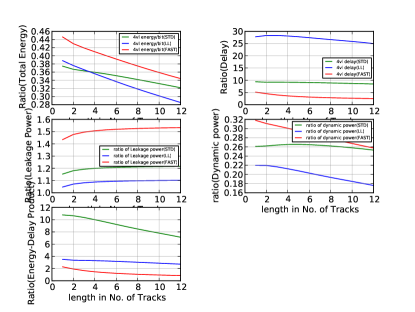
Figure 9 plots the energy and delay comparison of the quaternery routing tracks with that of binary tracks. We have optimized the 4-valued repeater circuits by varying the back-biasing with various different goals, namely FAST is optimized for delay, and LL is optimized for low leakage. STD is a compromise between the above two.
The plotted values are ratios of equivalent quantities w.r.t the value measured in the base architecture. The delay is measured from the switchbox multiplexer input to connection-box multiplexer output. We can see the energy and delay ratios for FAST and LL buffers are similar to those for quaternary tracks depicted in figure 6. except for leakage which is less. This is due to extra transistors in the binary bus-2 multiplexers which are absent in quaternary case. The leakage from these transistors compensate the high leakage of repeaters in part. For more details about multiplexer leakage please refer to [25].
The FAST buffer is optimized for delay by using higher FBB (Forward Body Bias), consequently it has higher leakage compared to other buffers.
For the LL repeater there is very little FBB in the driving transistors which reduces leakage, but the delay is much higher because of lower drain current .
We can also note that even for FAST buffer the delay is twice that of binary signalling. The reader might note that this is not necessarily a penalty, as a particular computation (e.g adder) synthesized in 4-valued logic will have a smaller critical path in terms of interconnect hops. However in this article we only concentrate on routing delays, and additional advantages of using a complete mutli-valued arithmetic/logic are out of scope of this article.
VI-B Transistor Count
Based on the architecture described in section V-A and the transistor counts for the basic blocks (see table V), we compare transistor count for routing resources in table VI. The mux count for each switchbox can be seen in figures 8(a) and 8(c). For each tile there are 16 input connection box Muxes (16:1).
| Binary FPGA with Bus-2 tracks | ||
|---|---|---|
| Resource | count | Transistor Count |
| Switchbox Muxes (BUS-2) | ||
| Buffers | ||
| Connection Box Muxes | 16 | |
| TOTAL | Transistors | 15552T |
| Quaternary FPGA | ||
| Resource | count | Transistor Count |
| Muxes 8 input | ||
| 4-valued Repeaters | ||
| Connection Box Muxes | 16 | |
| 4-2 Translator | 16 | |
| 2-4 Translator | 4 | |
| TOTAL | Transistors | 14484T |
From the above calculation we can see that even though the 4-valued repeaters are 1.5 times bigger in transistor count, the overall area reduction in the routing resources are of the order of 10 %. This is because quaternary tracks require less routing multiplexers. To account for layout complications we added a factor layout overhead factor. The layout overhead factor is around 10% (see sec. VIII).
VII Variability & Reliability
VII-A Process Variation
Process variation and signal integrity are increasingly important in recent technology nodes. FDSOI benefits from reduced variability thanks to absence of RDF (Random Dopant Fluctuation). However in the quaternary repeater circuits several transistor pairs are operated with VDD very close to the threshold Voltage, in that sense they are working in the near-threshold region. This makes them slightly more susceptible to process variation.
To evaluate this we conducted Monte-Carlo experiments with a length-6 tracks (hex Lines). We see that for quaternary tracks the Pelgrom coefficient of variation () is which is roughly twice that of the binary tracks ().
VII-B Sensitivity to Back-Bias Voltage
Sensitivity to back-bias voltage is a major concern for reliability. We conducted a sensitivity analysis w.r.t back bias voltage for the repeater and translator circuits. The circuits are functional upto a 10% variation in the . Recall that the sensitivity of to back bias volatge is 85 mv/V. However since very little current is drawn through the back bias port (pA) thanks to insulation, there is no reason to expect significant IR DROP in even in a big chip. There are other concerns such as transient noise on the back bias port but it is out of scope of this article.
VIII Layout
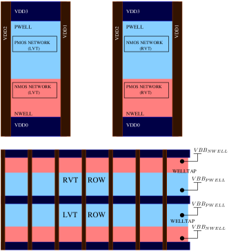
In fig. 11 we present an outline of the transistor/std. cell placements to implement multi-valued circuits. As seen in the circuit diagram(fig. 4) we have used both RVT (for Reverse Body-Bias) and LVT (for Forward Body Bias) transistors. Mixing LVT and RVT transistors generates a complicated layout as observed in [19]. However in our case we have an advantage that the back-biasing voltages are fixed, and we use the same for LVT and RVT transistors in PWELL and NWELL. Thus we can arrange RVT and LVT transistors in back to back rows which share a well. In this scheme we don’t need and extra isolation between these rows. A similar layout scheme is prescribed in [19].
Also we can see that the VDD2 and VDD1 supply lines are laid out vertically in metal level 2, and VDD3 (VDD in standard designs) and VDD0( GND in standard designs) are laid out in horizontal direction in metal level 1 as in traditional STD. Cell flows. The amount of routing area taken by the extra supply lines does not exceed 15% of the cell routing area in metal level 2. Given 6 signal routing layers we can expect a gain of 47% gain in overall wire routing area.
For design rule concerns the actual layout of the repeater is roughly 10% bigger than the layout size calculated based on transistor counts, so we use a layout factor (LOF) of in table VI to calculate the gain in transistor area.
IX Conclusion
Based on the above experimental results, for Quaternary signalling in an FPGA we can expect
-
•
40-50% reduction in wire routing area.
-
•
10% reduction in transistor area occupied by routing resources which is a major share of FPGA area.
-
•
3x reduction in dynamic power consumption, which is equivalent to CMOS operation in near-threshold [29].
There is also a penalty of leakage power. This can be mitigated by the use of low-leakage versions, or use of sleep modes.
Because of the above characteristics we can imagine the following usage scenarios for multi-valued tracks
-
•
Bus based FPGAs [28] have been reported where a bus of 4 gives the optimum area efficiency. These bus based tracks can be implemented as multi-valued tracks.
-
•
Higher order routing topologies (e.g Butterfly Fat Tree, Hypercube) which are limited by wire routing area [6].
-
•
Asynchronous logic which requires dual rail signalling and thus demanding in terms of routing [9].
-
•
Ultra low-energy FPGAs.
There could also be some concerns regarding the susceptibility to process variation. Several methods at higher levels of CAD are proposed [27, 10] to mitigate these problems. These methods have to be used in conjunction with multi-valued tracks.
Our future research direction will be to do a benchmark based study for FPGA architectures using multi-valued tracks, and leakage optimization of the circuits presented in this article.
References
- [1] V. Betz, J. Rose, and A. Marquardt, editors. Architecture and CAD for Deep-Submicron FPGAs. Kluwer Academic Publishers, Norwell, MA, USA, 1999.
- [2] H. Brian. Third base. In American Scientist, 2013, volume 89, page 490, 2001.
- [3] K. e. a. Cheng. Extremely thin soi (etsoi) cmos with record low variability for low power system-on-chip applications. In Electron Devices Meeting (IEDM), 2009 IEEE International, pages 1–4, Dec 2009.
- [4] T. I. Corporation. Intel strataflash(tm) memory technology. In Application Note AP-677, 1998.
- [5] R. Cunha, H. Boudinov, and L. Carro. Quaternary look-up tables using voltage-mode cmos logic design. In Multiple-Valued Logic, 2007. ISMVL 2007. 37th International Symposium on, pages 56–56, May 2007.
- [6] A. DeHon. Compact, multilayer layout for butterfly fat-tree. In Proceedings of the Twelfth Annual ACM Symposium on Parallel Algorithms and Architectures, SPAA ’00, pages 206–215, New York, NY, USA, 2000. ACM.
- [7] E. Dubrova. Multiple-valued logic in vlsi: Challenges and opportunities. In In Proceedings of NORCHIP’99, 1999.
- [8] C. H. et. al. A 125mhz burst mode 0.18/spl mu/m 128mbit 2 bits per cell flash memory. In VLSI Circuits Digest of Technical Papers, 2002. Symposium on, pages 304–307, June 2002.
- [9] T. Felicijan and S. Furber. An asynchronous ternary logic signaling system. Very Large Scale Integration (VLSI) Systems, IEEE Transactions on, 11(6):1114–1119, Dec 2003.
- [10] B. Gojman and A. DeHon. Grok-int: Generating real on-chip knowledge for interconnect delays using timing extraction. In Field-Programmable Custom Computing Machines (FCCM), 2014 IEEE 22nd Annual International Symposium on, pages 88–95, May 2014.
- [11] S. Hurst. Multiple-valued logic?its status and its future. IEEE Transactions on Computers, 33(12):1160–1179, 1984.
- [12] T. Ishii, H. Ito, M. Kimura, K. Okada, and K. Masu. A 6.5-mw 5-gbps on-chip differential transmission line interconnect with a low-latency asymmetric tx in a 180nm cmos technology. In Solid-State Circuits Conference, 2006. ASSCC 2006. IEEE Asian, pages 131–134, Nov 2006.
- [13] N. Jin, S.-Y. Chung, R. M. Heyns, P. R. Berger, R. Yu, P. E. Thompson, and S. L. Rommel. Tri-state logic using vertically integrated si-sige resonant interband tunneling diodes with double ndr. IEEE Electron Device Letters, 25(9):646–648, Sept 2004.
- [14] C. Lazzari, J. Fernandes, P. Flores, and J. Monteiro. An efficient low power multiple-value look-up table targeting quaternary fpgas. In Integrated Circuit and System Design. Power and Timing Modeling, Optimization, and Simulation, volume 6448 of Lecture Notes in Computer Science, pages 84–93. Springer Berlin Heidelberg, 2011.
- [15] G. Lemieux, E. Lee, M. Tom, and A. Yu. Directional and single-driver wires in fpga interconnect. In Field-Programmable Technology, 2004. Proceedings. 2004 IEEE International Conference on, pages 41–48, Dec 2004.
- [16] P. Magarshack, P. Flatresse, and G. Cesana. Utbb fd-soi: A process/design symbiosis for breakthrough energy-efficiency. In Design, Automation Test in Europe Conference Exhibition (DATE), 2013, pages 952–957, March 2013.
- [17] D. Miller. Rationale and challenges for optical interconnects to electronic chips. Proceedings of the IEEE, 88(6):728–749, June 2000.
- [18] obfuscated. obfuscated. In obfuscated, page obfuscated, obfuscated.
- [19] B. Pelloux-Prayer, A. Valentian, B. Giraud, Y. Thonnart, J. P. Noel, P. Flatresse, and E. Beigné. Fine grain multi-vt co-integration methodology in utbb fd-soi technology. In 2013 IFIP/IEEE 21st International Conference on Very Large Scale Integration (VLSI-SoC), pages 168–173, Oct 2013.
- [20] J. Qian, S. Pullela, and L. Pillage. Modeling the “effective capacitance” for the rc interconnect of cmos gates. Trans. Comp.-Aided Des. Integ. Cir. Sys., 13(12):1526–1535, Nov. 2006.
- [21] J. M. Rabaey. Digital Integrated Circuits: A Design Perspective. Prentice-Hall, Inc., Upper Saddle River, NJ, USA, 1996.
- [22] L. Shang, A. S. Kaviani, and K. Bathala. Dynamic power consumption in virtex™-ii fpga family. In Proceedings of the 2002 ACM/SIGDA Tenth International Symposium on Field-programmable Gate Arrays, FPGA ’02, pages 157–164, New York, NY, USA, 2002. ACM.
- [23] H. Shirahama and T. Hanyu. Design of high-performance quaternary adders based on output-generator sharing. In Multiple Valued Logic, 2008. ISMVL 2008. 38th International Symposium on, pages 8–13, May 2008.
- [24] K. Smith. The prospects for multivalued logic: A technology and applications view. Computers, IEEE Transactions on, C-30(9):619–634, Sept 1981.
- [25] S. Srinivasan, A. Gayasen, N. Vijaykrishnan, and T. Tuan. Leakage control in fpga routing fabric. In Proceedings of the 2005 Asia and South Pacific Design Automation Conference, ASP-DAC ’05, pages 661–664, New York, NY, USA, 2005. ACM.
- [26] S. Vitale, P. Wyatt, N. Checka, J. Kedzierski, and C. Keast. Fdsoi process technology for subthreshold-operation ultralow-power electronics. Proceedings of the IEEE, 98(2):333–342, Feb 2010.
- [27] H.-Y. Wong, L. Cheng, Y. Lin, and L. He. Fpga device and architecture evaluation considering process variations. In Computer-Aided Design, 2005. ICCAD-2005. IEEE/ACM International Conference on, pages 19–24, Nov 2005.
- [28] A. Ye and J. Rose. Using bus-based connections to improve field-programmable gate-array density for implementing datapath circuits. IEEE Trans. Very Large Scale Integr. Syst., 14(5):462–473, May 2006.
- [29] B. Zhai, R. G. Dreslinski, D. Blaauw, T. Mudge, and D. Sylvester. Energy efficient near-threshold chip multi-processing. In Proceedings of the 2007 International Symposium on Low Power Electronics and Design, ISLPED ’07, pages 32–37, New York, NY, USA, 2007. ACM.
Anonymous Reviews
Reviewer 1
I thought the idea in this paper was interesting but there are a large number
of issues that need to be corrected.

Counting area in transistors is not an acceptable way of comparing area between
the baseline and new architecture. As shown in Fig 1, the FDSOI with body bias
requires a body contact for each unique set of transistors sharing a Vdd. This
can potentially increase the area per transistor by perhaps 50\% in the case of
individual transistors. The paper needs a better area model that includes this.

I am not sure the paper deals fully with Vt and other variation. In addition to
the random variation of zero bias Vt0, there is also the variation of the body
effect between transistors. Since the paper is using body bias to adjust Vt by
~600mV, even a 10\% variation in body effect could add another 60mV of Vt
variation to each transistor beyond the variation at zero bias. Further, using
multiple power supplies creates the possibility of double ended variation. For
example with 50mV Vdd variation the 900mV supply could droop to 850mV, the
600mV supply boost to 650, leaving only 200mV Vgs for the Vdd to 2/3Vdd modes.
After adding in the two sources of Vt variation to the power supply variation,
are the circuits even operational?

I’m not sure why the routing muxes are shown as being controlled by quaterny or
standard Vdd binary. Since routing is controlled statically, the simplest
approach is to use a RAM cell powered by the Vdd boost voltage.

The paper makes several analyses of delay using power law models. I understand
that these are related to velocity saturated transistor drive currents and do
not think they are likely to be accurate in a low-Vdd regime. The only results
I would trust are SPICE models. SPICE is not mentioned in the paper anywhere so
it is not clear to me how the results were generated. Similarly it is unclear
how the leakage results are generated.

The paper fails to make an complete comparison between binary and quaternary by
only comparing the two power-delay points. Binary is much faster but 3X higher
power. However if I drop the Vdd of binary by a factor of 0.6X, it will slow
down and the dynamic power will reduce by 3X (0.6^2 = 0.36, about 3X
reduction). I will hazard a guess that binary at 0.6X Vdd is faster and same
power as quaternery, but this needs to be evaluated.
Reviewer 2
multiple values on sinals wires have been discussed for FPGAs for many years.
Most papers exploite the bandwidth by time-multiplexing rather than
multi-values.  Some discussion of the advantages of your method is warranted,
particularly since the tighter control required for multi-values is difficult
in advanced nodess.  Also your assumed performance permits significant time
multiplexing of binary values.

Section II.  A description of FDSOI is only necessary if your subsequent
analysis depends on it.

Where does table 1 come from?  The units in table 2 are unclear.
Fig 3 bubbles on inverters are much too small.

I have serious problems with your experimental procedure.  You propose a binary
architecture with the same architectural limitations imposed by your
multi-valued signaling.  Basically, you wipe out your major drawaback: the fact
that multi-valued signals must be routed together to share a wiring trace.
Modern binary FPGAs do not do that and achieve a performance, power and density
advantage.

This is absolutely not "fairness" (V.B paragraph 2).  Other architectures don’t
need to do it.        The penalties (performance, power, size) for bundling and
un-bundling signals needs to be incorporated into your result, but not the
result for the binary alternatives.

With this in mind, you need to report performance differences.        Ideally,
these would include those imposed by the architecutre, after place and route.
Reviewer 3
The authors propose using body-biased FDSOI technology to create multi-valued
routing tracks for FPGAs. The body bias is used to create transistors with
different Vt values that can respond to different voltage levels (they do
3-valued logic with 1/3 of Vdd steps, and 4-valued logic with 1/4 Vdd steps).
The logic on the FPGA is still binary: only routing (or a subset of it) is
proposed to be multi-valued. They claim that the routing area would decrease
both due to a reduction in the number of wires, as well as area reduction of
the buffers and repeaters. The circuits are explained well and the delay and
power models presented in Sec IV make sense.

The trouble starts with Section V. I expected to see SPICE simulations to
validate the idea. Vth values are bound to have variations. The graphs of Fig 8
do not tell the whole story. Is a chain of repeaters going to switch correctly?
Monte-Carlo simulations of the chain are needed.

Experimental results showing noise susceptibility have to be included. The
graphs of Fig 9 are inadequate: the authors could have done Monte-Carlo SPICE
simulations, modeling corss-talk and supply noise.

They only mention (in passing) methods to tackle cross talk, such as spacing
apart the wire segments more or limit the speed of operation. That would result
in partly defeating the purpose of multi-valued logic that they used to justify
their method in the first place. The effects of spacing and lower frequency to
achieve similar noise immunity as binary logic should be quantified and
compared.

Overall, I liked the idea presented in the paper, but I feel it needs to be
improved more to warrant publication. Even if the paper turns out to be a
negative-results paper, I d like to see it fleshed out.
Reviewer 4
The main premise of using multiple voltages to reduce the wire count is
interesting. In general, a technique like this would make more sense in a board
where high quality wires are a rare, valuable resource. But applying the
technique within a chip isnt unheard of. And the truth is that wires are not
scaling like transistors. Even if the metal design rules come down with
technology, scaling wires with the design rules kills performance. Modern
device costs can be dominated by metal, and more so for programmable devices
than ASICs. So reducing wires is important. That said, my biggest concern for
this paper is just the cost overhead. I expect the cost (including area, power
and delays) to driving and receiving these multi-voltage signals to be
enormously prohibitive compared to simple buffers. For me, the other issues are
secondary, and Id like to see the costs addressed up front and convincingly.