Quantum Interference Hybrid Single-Electron Transistor
The manipulation of single charge quanta in solid state systems has been a field of active interest for several decades GrabertDevoret1992 ; PhysRevB.53.13682 .
Thanks to Coulombic repulsion between electrons, single charges can be confined in small metallic islands yielding to the so-called Coulomb-blockade regime AverinLikharev1986 .
Many quantum phenomena, such as the tunneling effect Pekola2008 or the Josephson coupling in superconducting junctions Giazotto2011 , have been exploited so far to control the charging state of a conducting island, and enable a number of applications ranging from on-chip cooling PhysRevLett.99.027203 ; PhysRevLett.103.120801 ; PhysRevLett.98.037201 ; RevModPhys.78.217 and current generation PekolaRevModPhys2013 ; Giblin2012 ; POTHIER1991573 to single-photon detection app6020035 .
Yet, in all Coulombic systems the external control parameters play a crucial role and their exploitation requires sometimes a rather complex experimental configuration KellerAPL ; PhysRevB.64.235418 ; PhysRevLett.91.177003 ; PhysRevLett.100.177201 ; VartiainenAPL .
Here we show that quantum interference established in a superconducting nanowire Giazotto2010 can act as a control parameter providing a phase-tunable energy barrier which allows charge manipulation with enhanced functionalities Enrico2016 .
This additional degree of freedom for single electronics stems from the interplay between magnetic flux-dependent proximity effect GiazottoHeatModulatorAPL ; PhysRevApplied.2.024005 ; Heikkila2002 and charging levels discretization existing in a Coulomb-blockaded
island.
Our quantum interference nanostructure represents the first realization of an innovative superconducting hybrid single-electron transistor called SQUISET Enrico2016 in which the charge landscape is phase-coherently manipulated by an external magnetic flux.
The interferometric nature of the transistor adds new perspectives to single electronics making it a promising building block in quantum metrology Flowers1324 , coherent caloritronics MartinezPerezAPL ; GiazottoHeatModulatorAPL ; MartinezPerez2015quatris ,
and quantum information technology Quantum2010 .
When a short metallic nanowire (i.e., a weak-link) interrupts a superconducting (S) ring its electronic density of states (DOSs) is strongly modified by the proximity effect. The latter occurs owing to the intimate contact with the superconductor, and turns out to be controllable via a magnetic flux piercing the loop. This property is at the basis of the superconducting quantum interference proximity transistor (SQUIPT) DAmbrosio2015 ; Giazotto2010 ; PhysRevApplied.2.024005 ; Strambini2016 . In this context, the behavior of a fully-superconducting SQUIPT, i.e., where the nanowire itself is a superconductor, has been recently theoretically investigated Virtanen2016 . Specifically, it has been shown that when the nanowire length is smaller or comparable to the superconducting coherence length its DOSs is characterized by a flux-tunable BCS-like energy gap, , where is the zero-temperature energy gap of the superconducting ring, the magnetic flux piercing the loop, and Wb is the flux quantum. The above functional behavior for the gap has been proposed as the building block of an innovative Coulombic turnstile PhysRevLett.64.2691 called superconducting quantum interference single-electron transistor (SQUISET) Enrico2016 . In the SQUISET, the charging state of a metallic island, governed by Coulomb blockade, can be controlled by manipulating the DOSs of its source and drain electrodes made of two independent SQUIPTs. This defines a unique superconducting single-electron (SE) transistor in which SE injection occurs thanks to an external magnetic flux instead of the widespread electrostatic gating.
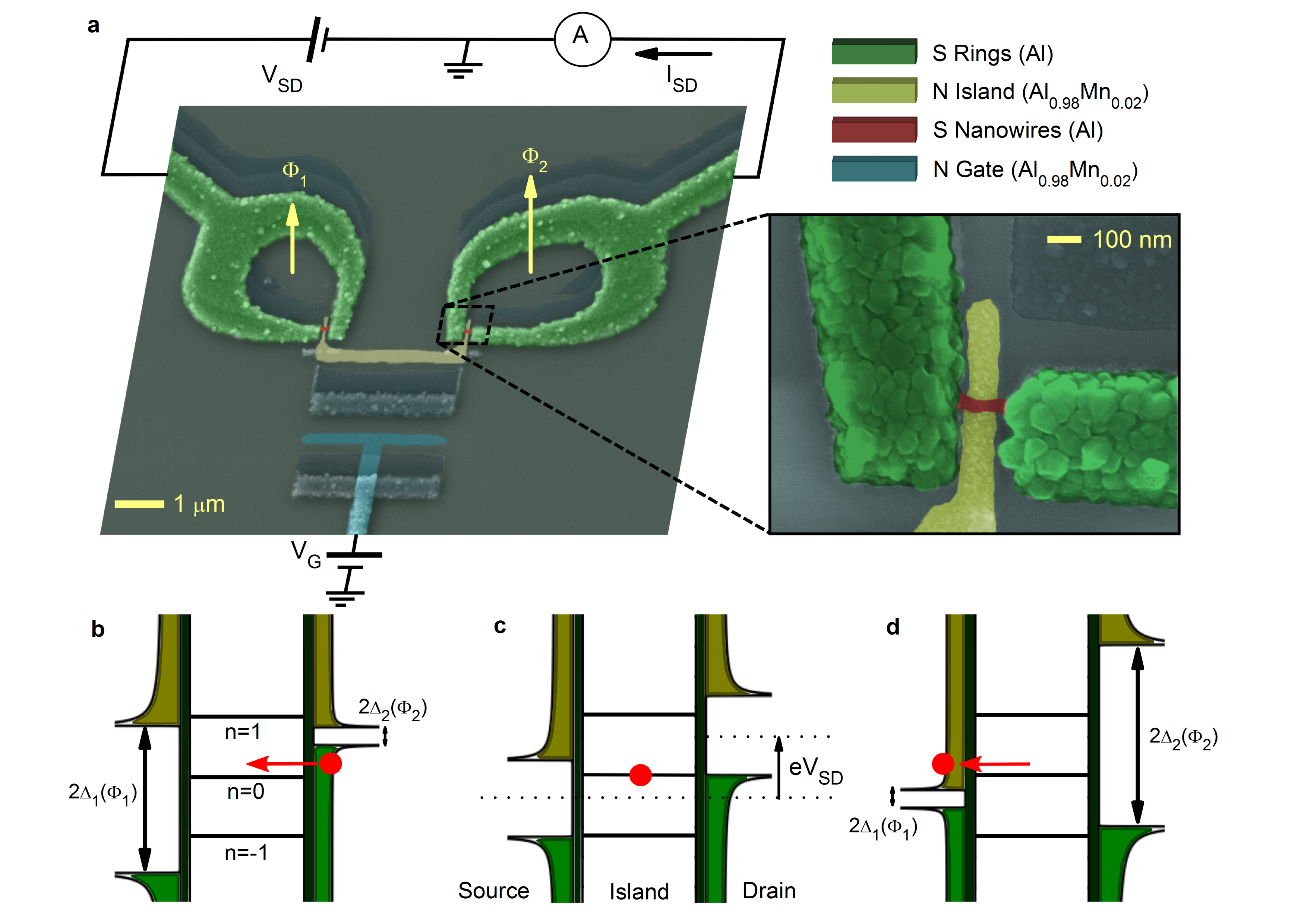
Here we report the first realization of the SQUISET and its phase-coherent magneto-electric characterization demonstrating its compatibility with a one-control parameter turnstile cycle. The SQUISETs are fabricated by standard three-angle shadow-mask PhysRevLett.59.109 deposition of metals through a conventional suspended resist mask (see Methods). A pseudo-color scanning electron micrography of the core of one typical device is shown in Fig. 1a. Two -nm-thick superconducting aluminum (Al) rings of different areas and are interrupted by two Al nanowires with length nm, thickness nm and width nm. At low temperature and zero magnetic field the energy gap in both nanowires is eV.
These nanowires realize the flux-tunable source and drain electrodes of the transistor, and are controlled by a single magnetic field () piercing the two S loops of different areas thereby yielding different magnetic fluxes and . The SE transistor is completed by a normal metal island (N) capacitively-coupled to a gate electrode, and electrically connected to the source-drain nanowires via two AlOx tunnel junctions with a normal-state resistance k. In the operating conditions, the SQUISET is voltage biased across the source-drain electrodes (), and the gate capacitor is polarized with elementary charges, where is gate voltage, is the gate-island capacitance, and is the electron charge. In this configuration a discrete number of SEs can be injected from the drain into the source electrode by operating the two magnetic fluxes and . Figures 1b-d sketch a typical clocking sequence illustrating the working principle of this SE transistor. A SE is first transferred from the drain into the island (Fig. 1b) where it is spatially localized owing to the finite charging energy (Fig. 1c) after which it is released into the source electrode (Fig. 1d).
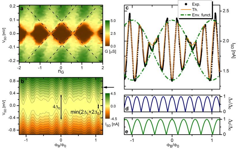
The charging energy of the island, the crucial parameter for SE protection, is first characterized independently from all the other elements of the SQUISET by quenching superconductivity in the device with a magnetic field mT (i.e., where is the Al critical field). In this condition the SQUISET behaves as a conventional SE transistor made of normal metal source-drain electrodes connected to a Coulombic island. From the ”ortodox” analysis of the stability diagram shown in Fig. 2a we estimate the system charging energy eV, the gate capacitance fF, and the source and drain capacitances ( fF). The nearly symmetric Coulomb-blockade diamonds of the diagram and the resulting source and drain capacitances confirm the similarity between source and drain tunnel junctions, an important condition for the optimal functionality of the SQUISET Enrico2016 . At lower field (), superconductivity is recovered in the source and drain electrodes leading to an extension of the blockade region of , where and are the energy gaps in the two nanowires. This appears in Fig. 2b showing the evolution of on and . Here, we have conveniently normalized by introducing the beating magnetic flux, , which describes the behavior of the transistor in the magnetic field, i.e., beating-like oscillations of the blockade regions and , as clearly visible in the envelope functions displayed in Fig. 2c. A frequency analysis of these oscillations allows to deduce the loops areas, m2 and m2 (see Methods).
With the aid of the above quantities and the theoretical model for the SQUIPT Virtanen2016 we can determine the flux-dependent behavior of the energy gaps in the two superconducting nanowires (see Figs. 2d-e). Then, the source-drain current flowing through the SQUISET () is obtained through the “ortodox” theory of quantum tunneling (see Methods) Enrico2016 . The good agreement between the theoretical and the experimental shown in Fig. 2c confirms the validity of our analysis
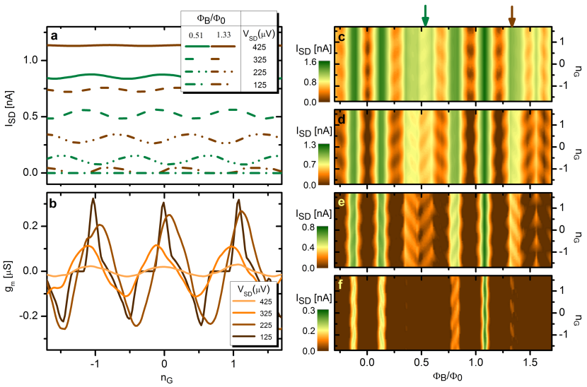
Having identified independently the role of and in the Coulomb-blockade operation of the transistor (see Figs. 2a,b), we now investigate the interplay between these two physical quantities for the control of the island charging state. In conventional Coulombic islands the latter is usually characterized through Coulomb oscillations (see Fig. 3a and b), where an imposed source-drain voltage () define the energy band for the island charge states which, controlled by the gate voltage, transports the current through the transistor. As shown before, in our device this energy band is reduced by the flux-tunable superconducting energy gaps as a result of their beating-like behavior in which modulates as well the Coulomb oscillations. The role of the gate control parameter is confirmed by Fig. 3b where, for a chosen condition () for which and are small and almost in phase, the transconductance is maximized around integer values of , and minimized for half-integer values. As a consequence of the small value of , the smaller is the more pronounced is the gate effect.
This interplay is clearly shown in Figs. 3c-f which display the Coulomb oscillations vs and for selected values of source-drain voltage ( V, V, V, and V from top to bottom, respectively). For large values of (see Fig. 3c), source-drain current is not blocked in the whole space of parameters apart from small lobes (two-dimensional analogue of the Coulomb peaks) located at with periodicity, and unitary periodicity in . In these conditions the two superconducting energy gap are in-phase at their maximum while the gate voltage modulates the current from a blockaded (brown) to a conducting region (orange). At lower bias voltages (see Fig. 3d-f) extended plateaus of zero current appear nearby and due to the reduced available energy which is not sufficient to transfer any electron across the tunneling barriers. Accordingly, the Coulomb lobes are shifted in magnetic flux reaching the regions of and for eV. These are the relevant regions that experimentally demonstrate the capability of our device to operate in a magnetic-flux subspace condition, where the two energy gaps and are almost in anti-phase (see Fig. 2d-e) with respect to their own magnetic fluxes (). At very low bias ( Fig. 3f) the current is still finite for some specific magnetic-field values, with a maximum occurring at which corresponds to the value that minimizes the sum (see Fig. 2d,e). This value is consistent as well with the minimum observed in the stability diagram of Fig. 2b.
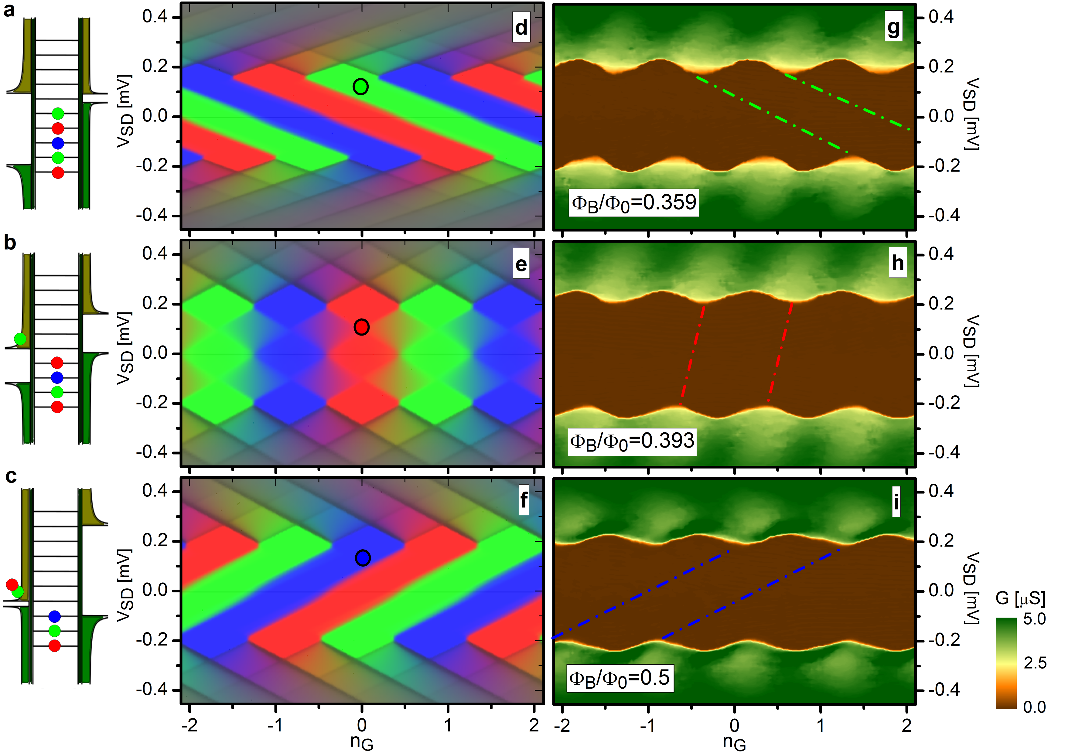
We now show the experimental evidence of the turnstile configuration capability of our SE transistor in the anti-phase regime (i.e., at ) which represent the optimal operating condition, as shown in the sketch of Fig. 1b-d. In this specific device the charging energy is smaller than the nanowires gaps () so that more than one single charge can be loaded and unloaded in the island per operating quasi-static cycle. This mechanism appears clearly from Figs. 4a-c where the energy band diagrams of the island are displayed for the magnetic configurations explored. Red-green-blue (RGB) colors are associated to each single energy level of the Coulombic island, and these are recalled in Figs. 4d-f representing the calculated stability diagrams for the probability to have one electron in the last occupied energy level. Pure RGB colors denote regions where island charge states are blocked and thereby suitable for a high-fidelity SE turnstile operation. Color mixing identifies those situations where the charge configuration of the island is not fixed, and a ‘leakage’ current can flow through the transistor.
The experimental confirmation of this physical picture is provided by the stability diagrams of the differential conductance measured in these three magneto-static configurations (see Figs. 4g-i). The diagrams show a specific skewing of Coulomb diamonds which evolves continuously as a function of the magnetic flux, in full agreement with the calculations (see Figs. 4d-f), and stemming from the asymmetry of the energy gaps in the nanowires (). Within this flux sequence the transistor can therefore operate as a SE turnstile by fixing the bias voltage in the blockade region of interest (e.g., at , as indicated by the black circles in Figs. 4d-f), and by sweeping the external magnetic flux. In the present quasi-static situation, the sequence starts at by loading five electrons into the island (Fig. 4a), and ends at where two electrons are unloaded from the island. This specific example demonstrates the possibility to control the transfer of two electrons from drain to source without using the gate voltage. By experimental evidence it is clear how a magnetic flux cycle allow the control of a discrete number of electron flow between the source and the drain electrode.
We wish to further stress the role embodied by the magnetic flux as a control parameter: our experimental results prove indeed that a SQUISET having a rather simple design can reach the turnstile capability for single charge quanta with a suitable magnetic-like gating.
In summary, we have realized the first superconducting quantum interference single-electron transistor (SQUISET) where the magnetic flux degree of freedom provides an additional control over single-electron charge transfer. The transistor can be realized with conventional nanofabrication techniques, and can be integrated with on-chip superconducting coils for independent magnetic flux control, fast turnstile operation and enhanced functionalities. Operating the device with a high-frequency electromagnetic field will provide a promising route towards the metrological definition of the current standard. In this view the transport physics of the device proposed is, at first order, comparable to the well-known SINIS Pekola2008 turnstile with which it shares the possible pumping error sources. Moreover, the detrimental effects of the background charges fluctuations PhysRevB.53.13682 on the accuracy of metallic turnstiles could potentially be reduced in our SQUISET respect to other electrically gated coulombic structures since the two-level systems responsible for such fluctuations should be quiet under magnetic time-dependent excitation. The SQUISET might have impact in cryogenic micro- and nanoelectronics as well as in solid-state quantum information technologies. Extending the concept here presented to a fully superconducting structure, the charge configuration of a superconducting island could be magnetically adiabatically tuned exploiting its Josephson coupling PhysRevLett.91.177003 ; Quantum2010 with two SQUIPT-engineered electrodes Virtanen2016 . Yet, combined with superconducting circuits, it could act as a building block of future coherent single nanoelectronics.
Methods
Experimental - One step of electron-beam lithography was used to fabricate the transistors followed by a three-angle shadow-mask evaporation of metallic thin films through a suspended resist mask. The latter, lying onto an oxidized Si substrate, was processed in a UHV electron-beam evaporator. A -nm-thick layer of Al was initially deposited, the chip being tilted at an angle of , to realize the normal metal island structure. The sample was then exposed to mbar O2 for min to form the AlO thin insulating layer composing the tunnel junctions. Then the chip was tilted to , and a -nm-thick layer of Al was deposited to form the superconducting nanowires. Finally, a -nm-thick layer of Al was deposited at to realize the superconducting rings. The source and the drain electrodes are nominally identical differing only for the rings areas.
The magneto-electric characterization of the SQUISETs was performed down to mK in a shielded and filtered dilution refrigerator. Current and conductance measurements were performed with room temperature electronics whereas the magnetic field was imposed through a superconducting coil surrounding the sample chamber.
Theory The theoretical modeling of the SQUISET was performed in the framework of the ”orthodox theory’ of single-electron tunneling under the static regime condition. The sequential tunneling approach in the first order approximation leads to the charge current as a solution of the standard master equation GrabertDevoret1992 :
| (1) |
where are the free energy variations associated to a single electron tunneling event in the -th junction that increase () or decrease () the number of excess charges on the island (), and are the tunneling rates across the first junction. Moreover, is the probability to find the transistor in the charging state depending on its electro-magnetic environment. The full expressions for the above quantities can be found in Enrico2016 . We assumed each component of the transistor to be at thermal equilibrium with the lattice phonons, and to reside at the base temperature of the cryostat. Subgap quasiparticles populations in the source and drain electrodes have been modeled by assuming a superconducting density of states smeared by a Dynes parameter Dynes1984 ; PhysRevLett.105.026803 . The magnetic fluxes, , have been deduced assuming a uniform magnetic field perpendicular to the SQUIPTs loop plane, and rings areas () coming from the geometrical estimate. Moreover, the two areas were also deduced by peak analysis on the FFT trace of the current vs magnetic field signal, the latter revealing two primary components related to the different superconducting loops.
References
References
- (1) Grabert, H. & Devoret, M. H. (eds.) Single Charge Tunneling: Coulomb Blockade Phenomena in Nanostructures (Kluwer Academic / Plenum Publishers, New York, 1992).
- (2) Zorin, A. B. et al. Background charge noise in metallic single-electron tunneling devices. Phys. Rev. B 53, 13682–13687 (1996).
- (3) Averin, D. V. & Likharev, K. K. Coulomb blockade of single-electron tunneling, and coherent oscillations in small tunnel junctions. J. Low Temp. Phys. 62, 345–3730 (1986).
- (4) Pekola, J. P. et al. Hybrid single-electron transistor as a source of quantized electric current. Nat. Phys. 4, 120–124 (2008). Letter.
- (5) Giazotto, F. et al. A josephson quantum electron pump. Nat. Phys. 7, 857–861 (2011).
- (6) Saira, O.-P. et al. Heat transistor: Demonstration of gate-controlled electronic refrigeration. Phys. Rev. Lett. 99, 027203 (2007).
- (7) Kafanov, S. et al. Single-electronic radio-frequency refrigerator. Phys. Rev. Lett. 103, 120801 (2009).
- (8) Pekola, J. P., Giazotto, F. & Saira, O.-P. Radio-frequency single-electron refrigerator. Phys. Rev. Lett. 98, 037201 (2007).
- (9) Giazotto, F., Heikkilä, T. T., Luukanen, A., Savin, A. M. & Pekola, J. P. Opportunities for mesoscopics in thermometry and refrigeration: Physics and applications. Rev. Mod. Phys. 78, 217–274 (2006).
- (10) Pekola, J. P. et al. Single-electron current sources: Toward a refined definition of the ampere. Rev. Mod. Phys. 85, 1421–1472 (2013).
- (11) Giblin, S. P. et al. Towards a quantum representation of the ampere using single electron pumps. Nat. Commun. 3, 930 (2012).
- (12) Pothier, H. et al. Single electron pump fabricated with ultrasmall normal tunnel junctions. Physica B: Condensed Matter 169, 573 – 574 (1991).
- (13) Jalali-Jafari, B., Lotkhov, S. V. & Zorin, A. B. Detection of on-chip generated weak microwave radiation using superconducting normal-metal set. Applied Sciences 6, 35 (2016).
- (14) Keller, M. W. et al. Accuracy of electron counting using a 7‐junction electron pump. Appl. Phys. Lett. 69 (1996).
- (15) Shimada, H. & Ootuka, Y. Magnetic-field-driven single-electron pump. Phys. Rev. B 64, 235418 (2001).
- (16) Niskanen, A. O., Pekola, J. P. & Seppä, H. Fast and accurate single-island charge pump: implementation of a Cooper pair pump. Phys. Rev. Lett. 91, 177003 (2003).
- (17) Möttönen, M., Vartiainen, J. J. & Pekola, J. P. Experimental determination of the Berry phase in a superconducting charge pump. Phys. Rev. Lett. 100, 177201 (2008).
- (18) Vartiainen, J. J. et al. Nanoampere pumping of Cooper pairs. Appl. Phys. Lett. 90 (2007).
- (19) Giazotto, F., Peltonen, J. T., Meschke, M. & Pekola, J. P. Superconducting quantum interference proximity transistor. Nat. Phys. 6, 254–259 (2010).
- (20) Enrico, E. & Giazotto, F. Superconducting quantum interference single-electron transistor. Phys. Rev. Applied 5, 064020 (2016).
- (21) Giazotto, F. & Martinez-Perez, M. J. Phase-controlled superconducting heat-flux quantum modulator. Appl. Phys. Lett. 101 (2012).
- (22) Ronzani, A., Altimiras, C. & Giazotto, F. Highly sensitive superconducting quantum-interference proximity transistor. Phys. Rev. Appl. 2, 024005 (2014).
- (23) Heikkilä, T. T., Särkkä, J. & Wilhelm, F. K. Supercurrent-carrying density of states in diffusive mesoscopic josephson weak links. Phys. Rev. B 66, 184513 (2002).
- (24) Flowers, J. The route to atomic and quantum standards. Science 306, 1324–1330 (2004).
- (25) Martinez-Perez, M. J. & Giazotto, F. Efficient phase-tunable josephson thermal rectifier. Appl. Phys. Lett. 102 (2013).
- (26) Martinez-Perez, M. J., Fornieri, A. & Giazotto, F. Rectification of electronic heat current by a hybrid thermal diode. Nat. Nanotech. 10, 303–307 (2015).
- (27) Nielsen, M. A. & Chuang, I. L. (eds.) Quantum Computation and Quantum Information (Cambridge University Press, Cambridge, 2000).
- (28) Virtanen, P., Ronzani, A. & Giazotto, F. Spectral characteristics of a fully-superconducting SQUIPT. Phys. Rev. Appl. 6, 054002 (2016).
- (29) D’Ambrosio, S., Meissner, M., Blanc, C., Ronzani, A. & Giazotto, F. Normal metal tunnel junction-based superconducting quantum interference proximity transistor. Appl. Phys. Lett. 107 (2015).
- (30) Strambini, E. et al. The -SQUIPT as a tool to phase-engineer Josephson topological materials. Nat. Nanotech. 157 (2016).
- (31) Fulton, T. A. & Dolan, G. J. Observation of single-electron charging effects in small tunnel junctions. Phys. Rev. Lett. 59, 109–112 (1987).
- (32) Geerligs, L. J. et al. Frequency-locked turnstile device for single electrons. Phys. Rev. Lett. 64, 2691–2694 (1990).
- (33) Dynes, R. C., Garno, J. P., Hertel, G. B. & Orlando, T. P. Tunneling study of superconductivity near the metal-insulator transition. Phys. Rev. Lett. 53, 2437–2440 (1984).
- (34) Pekola, J. P. et al. Environment-assisted tunneling as an origin of the dynes density of states. Phys. Rev. Lett. 105, 026803 (2010).
Acknowledgements
We thank S. D’Ambrosio, I. Mendes, G. Amato and L. Callegaro for useful discussions. E.E. acknoledges partial financial support from the European Metrology Research Programme (”EXL03 MICROPHOTON”). The EMRP is jointly funded by the EMRP participating countries within EURAMET and the European Union. The work of E.S. is funded by the Marie Curie Individual Fellowship MSCAIFEF-ST No. 660532-SuperMag. F.G. acknowledges the European Research Council under the European Unions Seventh Framework Program (FP7/2007- 2013)/ERC Grant agreement No. 615187-COMANCHE, and MIUR-FIRB2013-Project Coca (Grant No. RBFR1379UX) for partial financial support.
Author contributions
E.E. fabricated the samples and carried out simulations. E.E. and E.S. performed the measurements and analysed the data. E.E. and F.G. conceived the experiment. E.E., E.S. and F.G. discussed the results and implications equally at all stages, and wrote the manuscript.