Geometry dependence of 2-dimensional space-charge-limited currents††thanks: 2016. This manuscript version is made available under the CC-BY-NC-ND 4.0 license http://creativecommons.org/licenses/by-nc-nd/4.0/
Abstract
The space-charge-limited current in a zero thickness planar thin film depends on the geometry of the electrodes. We present a theory which is to a large extent analytical and applicable to many different lay-outs. We show that a space-charge-limited current can only be sustained if the emitting electrode induces a singularity in the field and if the singularity induced by the collecting electrode is not too strong. For those lay-outs where no space-charge-limited current can be sustained for a zero thickness film, the real thickness of the film must be taken into account using a numerical model.
Ghent University, Dept. ELIS, Liquid Crystals & Photonics
Technologiepark–Zwijnaarde 15, B-9052 Gent
Patrick.DeVisschere@UGent.be
1 Introduction
When charge carriers are injected into an electrically poorly conducting medium, the current is space-charge-limited and when the medium has Ohmic conductivity, with increasing voltage, the current eventually becomes also space-charge-limited. This phenomenon has been known for a long time in a one-dimensional (1D) setting as described by the Mott-Gurney equation [1]
| (1) |
with the voltage, the current density, the width of the insulator, it’s dielectric constant and the mobility of the carriers. Eq. (1) holds in particular for single carrier injection under perfect injection conditions, meaning that the electric field is zero at the injecting electrode. Similar behavior has been observed in a planar two-dimensional (2D) setting in organic thin films [2, 3, 4, 5] and more recently in several types of monolayers [6, 7]. In [8] we derived the following 2D version of eq. (1) for an infinitesimally thin layer between two semi-infinite co-planar electrodes
| (2) |
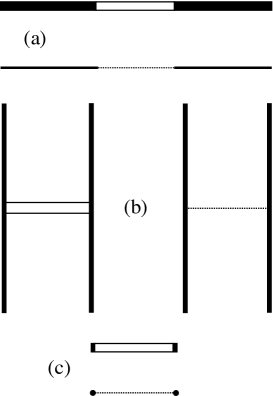
where is the surface current density, and similar additional results were also obtained for a photoconductor. Subsequently we discovered a paper by Grinberg e.a. [9] where besides this “strip” lay-out two more lay-outs were considered: a thin film between two parallel electrodes perpendicular to the film (“plane” lay-out) and a thin film with small “edge” electrodes. These lay-outs are shown in Fig. 1 together with the idealized models used to calculate the current. Indeed only “the limiting case of a vanishing film thickness” was considered and the relevant equations were solved numerically with the aim to obtain the prefactor occurring in the general expression
| (3) |
They found respectively , and . When we applied our analytical method to these idealized “plane” and “edge” models we found that actually , meaning that in these idealized structures no space-charge-limited (SCL) current can be sustained and to obtain a practical result the film thickness must be taken into account.
In this paper we explore the dependence of the prefactor in (3) on the lay-out systematically and analytically as much as possible. In section 2 we explain our method by deriving the value of for the reference case of two semi-infinite coplanar electrodes. In section 3 this result is extended to other lay-outs using conformal transformations and as a result we obtain several limits leading to the zero result for the “plane” lay-out. In section 4 we consider an approximate and numerical model for a thin film between planar electrodes but with a non-zero thickness. In section 5 we turn our attention to electrodes with finite width, in particular the idealized “edge” electrodes. In this case a slightly different method must be used and a single numerical integration is required to find . In the last section 6 we consider asymmetrical lay-outs.
In their paper Grinberg e.a. refer to a paper by Geurst [10] where the exact expression for the prefactor occurring in (2) for the “strip” lay-out was derived, as far as we know, for the first time. This result was found by solving analytically a boundary value problem for the square of the complex electric field. In our method [8] the problem is reduced to solving a non-linear integral equation with a known solution, which was published by Peters [11]. We will also show how these two methods are related. A totally different approach to the problem, based on E-Infinity theory, was published by Zmeskal e.a. [12].
Eq. (1)-(3) and the rest of this paper holds for drift transport. For ballistic transport eq. (1) must be replaced by the (1D) Child-Langmuir law. Some studies of 2D versions of the Child-Langmuir law have been published for parallel electrodes [13, 14, 15, 16, 17]. In what follows we consider the injection of positive charges from the anode (emitter) to the cathode (collector) but the results are obviously equally valid for negative charges.
2 Semi-infinite coplanar electrodes
Photoconductors are often contacted by two interdigitated electrodes and if the fingers are much wider than the gaps in between then this lay-out can be approximated well by two semi-infinite coplanar electrodes as shown in Fig. 2.
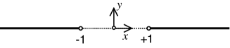
In the calculations we will use only normalized quantities with the channel width and the applied voltage . The true surface current density is then written as
| (4) |
where the in-plane component of the electric field and the upper out-of-plane component , with the surface charge density, are normalized by . Comparing with (3) we then find the prefactor from the equation
| (5) |
where the field components must still satisfy Maxwell’s equations. Assuming known for all , and using the Green’s function, is easily found as
| (6) |
where the integral is a Cauchy principal value integral. From this equation we learn that both field components are connected by a Hilbert-transform over the real axis. Since the Hilbert-transform equals it’s own inverse, except for a sign reversal, we find immediately
| (7) |
where we also used the boundary condition that along the electrodes . Substituting (7) in (5) we find that the unknown function most be chosen in such a way that the following expression
| (8) |
is a constant within the gap and zero elsewhere. This type of equation can be solved analytically [8, 11] but to obtain the explicit solution is not needed (in section 5 we explain how the field components can be obtained). It suffices to integrate (8) over the gap after removing possible singularities. This condition is necessary for reversing the order of integration in the rhs111Formally if , with [18]. Since we need .. In this particular case the in-plane component of the electric field shows a singularity near only, whereas because of the perfect injection boundary condition. Multiplying eq. (8) with the factor and integrating we obtain
| (9) |
Reversing the order of integration and splitting the last integral by rewriting as then yields
| (10) |
According to (9) the first term on the rhs equals and from the boundary condition we know that and we find .
3 Lay-outs conformally similar with 2 semi-infinite coplanar electrodes
Since we are dealing with a two-dimensional field problem, we can use conformal transformations to obtain the field for additional lay-outs of the electrodes [19, 20]. A straightforward generalization of the reference structure in Fig. 2 and which is also conformally similar is shown in Fig. 3a, with . Using coordinates eq. (5) is still valid after replacing the coordinates
| (11) |
but the relation between both field components is now more complicated. However by transforming the lay-out of Fig. 3a to the reference lay-out of Fig. 2 by a conformal transformation we can solve the equation in the -domain of Fig. 2 instead. Indeed from the conformality it follows that voltage drop as well as the charge density are conserved meaning that along the real axes
| (12) |
| (13) |
and eq. (11) becomes
| (14) |
where the latter must be solved in the reference lay-out of Fig. 2 for which the field solutions (6) and (7) can be used. This equation can still be solved with the technique of Peters [11] and in particular we obtain after integration over the channel
| (15) |
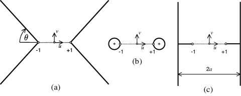
The prefactor is thus easily found for every lay-out conformal with the reference lay-out, supposed the transformation for the channel can be found. For the sharply bend (“wedge”) electrodes in Fig. 3a the conformal transformation can be found in terms of the hypergeometric function with in particular
| (16) |
where is the gamma function. We then obtain applying (15)
| (17) |
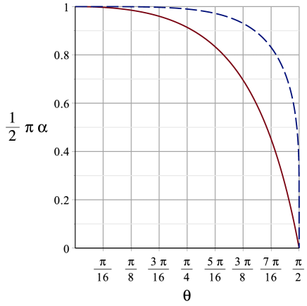
with . As can be seen in Fig. 4 the value of drops relatively slowly for small values of and for a total opening angle of the value of is still nearly 90% of it’s maximum value. When the bend angle approaches zero, the value drops fast to zero. Both limits are given by
| (18) | ||||
| (19) |
For the singularity in the field due to the electrode disappears and apparently no stable SCL current can be sustained without this singularity. This can be understood as follows: the field near the anode due to the space charge only, is directed towards the anode and this field as well as the charge density itself diverge. However the total charge induced in the anode is finite and if the anode is smooth the field due to the charge on the anode remains finite and therefore cannot overcome the diverging field due to the space charge. Stationary emission of holes into the gap is only possible if the field due to the charge on the anode also diverges. This will also be true for any pair of electrodes with a smooth surface, like e.g. the circular cylinders shown in Fig. 3b. In this case the conformal transformation yields
| (20) |
where is a constant depending on the radius of the cylinders. Due to the last factor the integral in the rhs of (15) diverges and .
Another lay-out with the required singularity and with a limit leading to the idealized “plane” lay-out is shown in Fig. 3c for which one finds with a simple Schwartz-Christoffel transformation that
| (21) |
with . With (15) we then find
| (22) |
with . In this case the drop of with increasing is even more robust with staying above 90% of it’s limiting value as long as the combined width of the electrode extensions is at least 25% of the gap width (). On the other hand the value of drops much faster to zero if the extension becomes much shorter. Both limits are given by
| (23) |
| (24) |
We have shown that for the idealized “plane” lay-out, shown on the right side in Fig. 1b, no stable SCL current can be sustained and therefore this is not an adequate model for the practical “plane” lay-out shown on the left. To calculate the SCL current for a thin film between parallel electrodes, the thickness of the film must necessarily be taken into account and for best results this requires a full blown numerical 2D model.
4 Non-vanishing film thickness
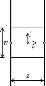
However for a film with finite thickness between parallel electrodes (Fig. 5), an approximate value can be obtained resorting to a one-dimensional numerical calculation only, if we neglect the variation of the space charge density in the direction perpendicular to the film [21].
The electric field of a unit line charge placed between 2 parallel electrodes at zero potential, and taken in the direction perpendicular to these plates is given by [9, 22]
| (25) |
where are the coordinates of the field point and those of the source point. Considering a film and assuming that the charge density is uniform in the -direction, we calculate the average Green’s function by averaging this field
| (26) |
where as before we moved the factor into the charge density, and where the latter is defined per unit area, hence the additional factor . This expression eventually leads to the closed form expression
| (27) |
where some care must be taken with the definition of the -function. The (normalized) field on the horizontal centerline can then be written as
| (28) |
with the charge density per unit area in the film. In this way the film with thickness can again be treated as a film with infinitesimally small thickness provided we use a modified Green’s function. Using as the unknown function, the prefactor can be found by solving the equation
| (29) |
which should be a constant for . Since the relation between the charge density and the electric field is no longer a simple Hilbert transform, this equation must be solved numerically. We have implemented two different methods for solving this equation: a general method which becomes time-consuming for very small values of and a series expansion method valid for .
In the first method eq. (29) is discretized after scaling the charge density and the electric field by , so that , and which can then be rewritten as
| (30) |
Since at least formally this can also be written as
| (31) |
This is a non-linear Hammerstein integral equation which we have solved with a simple collocation scheme [23]. Introducing a partition of the interval the unknown function is approximated by a sum , where the basis functions are associated with the nodes . We use a linear approximation (hat functions) except for the first node where we take into account the divergent nature of the charge density and use , being the width of the first element. A discrete set of equations is obtained by evaluating (31) at the nodes . These non-linear equations are then solved with the Newton-Krylov solver nsoli.m222http://www4.ncsu.edu/~ctk/newton/SOLVERS/nsoli.m.
In the 2nd method, we expand the charge density and the electric field as a series in a small parameter (not to be confused with the dielectric constant) as follows
| (32) |
| (33) |
where and are unknown functions except for , and which are related by
| (34) |
and keeping only the lowest order constant term we find the remaining relations between these coefficients, e.g. . In this way the functions and can be calculated sequentially. After terminating the series, is found by applying the boundary condition , which is a polynomial equation in , with a single real root. Finally we find .
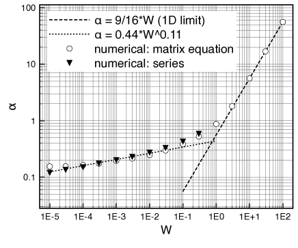
The results in Fig. 6 show that the 1D-limit () is approached closely if the thickness equals the width (). From consecutive approximations we’ve found that the series solution approaches the solution from above and this is compatible with the result found with the other method in the range . For smaller ’s the number of elements is insufficient to guarantee an accurate result with the first method. However for more elements this method becomes prohibitively time consuming. The combined results show that for sufficiently small , drops very slowly, approximately as and therefore that the current density increases as . This result should still be handled with some caution since it is based on the assumption of a uniform charge density and similar but also approximate calculations for ballistic transport have shown that this is not the case [14, 16].
5 Finite width electrodes
Returning again to a film with zero thickness, we consider in addition electrodes with negligible dimensions. This model is used by Grinberg e.a. [9] to simulate a thin film with “edge” contacts (Fig. 1c). It has the advantage that the electrodes can be treated simply as line charges. Due to the boundary condition at the anode, the anodic line charge must be zero and therefore the cathodic line charge must compensate the total (in our case positive) space charge in the film. Unfortunately the electric field of this cathodic line charge diverges and is not integrable, meaning that, contrary to what Grinberg e.a. found, again no stable SCL current can be sustained in this idealized structure. We arrive at the same conclusion by considering the limit of the structure in Fig. 3c when the radius of the electrodes goes to zero. As we have seen in this case no stable space charge can be sustained whatever the radius of the electrodes.
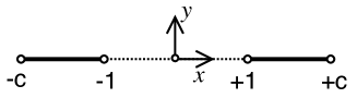
As an alternative model for a film with small electrodes we consider a lay-out with planar electrodes but with a finite width (Fig. 7), where we expect considering the foregoing that .
We rewrite (6) as
| (36) |
since outside the electrodes () no space charge occurs. Further we obtain
| (37) |
for the same reason and since in addition on the electrodes . Combining (36) and (37) and setting we must solve
| (38) |
Once more a useful relation is obtained by integrating this expression, provided one first removes the singularities so that the order of integration can be reversed. Since this time the charge density is the unknown function, we must also take into account a possible singularity for , therefore
| (39) |
and we then obtain
| (40) |
where and are the first and second order (dipole and quadrupole) moments of and we have taken into account that the zeroth order moment . We also introduced . Since these moments are not known beforehand, this time (40) is not sufficient to determine . The complete solution can be obtained if besides multiplying (38) with we also introduce a 2nd Hilbert transform as follows
| (41) |
where is used as an additional real integration variable. The order of the two Cauchy principal value integrals in the lhs can be reversed by using the Poincaré-Hardy-Bertrand theorem [24] and after some calculations (41) can be reduced to
| (42) |
Using (40) and expanding the remaining integral we find
| (43) |
Since on both sides of , the rhs of (43) must remain negative when passes through the point -1 and therefore in the rational term between brackets the pole should be compensated by a corresponding zero, meaning that
| (44) |
and with (40)
| (45) |
and finally
| (46) |
It’s now clear that near the charge density remains integrable and therefore we could have omitted in (39) the factor in . In that case and would not have occurred and instead of (40) and (43) we would have found (45) and (46) immediately.
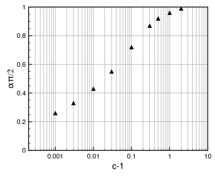
Combining (46) with (37) and can be calculated in the plane up to a scaling factor which can be determined numerically by the condition that . As shown in Fig. 8 the value of depends rather weakly on the width of the electrodes. For an electrode width equal to the width of the thin film ( the SCL current very nearly reaches it’s maximum value and this value reduces to 50% for electrodes with a width of approximately 1% of the width of the thin film ().
Knowing or on the real axis () is sufficient to determine the field in the rest of the plane. If we introduce the complex electric field , then just above and below the real axis and after squaring , which can be obtained by combining Eqs. (46) with (37). As explained by Peters [11] this expression is then readily extended to the whole -plane
| (47) |
With some hindsight we can obtain the same result much faster by applying the method used by Geurst [10] for the infinite “strip” lay-out (). Since is analytic outside the strip and according to (37) is a known constant on this segment, the square of the field must be of the form
| (48) |
where the first part solves the non-homogeneous problem and the rational function is the most general solution of the homogeneous problem. This rational function must tend to zero at infinity and can only contain poles at the extremities of the electrodes, but we have immediately taken into account that no pole occurs for . The unknown coefficients and can be found by considering the limit for . With the (normalized) dipole moment one finds readily that and by expanding the expression between the brackets in (48) and equating corresponding terms one finds , , , in agreement with (47), as well as (45).
6 Asymmetric electrodes
From the foregoing we have learned that of the 3 lay-outs shown in Fig. 1 only the “strip” lay-out can sustain a stable SCL current. However the reasons for the absence of a stable SCL current between (idealized) “plane” and “edge” electrodes are totally different: the “plane” lay-out fails because of a missing singularity in the field of the emitting electrode, whereas the “edge” lay-out fails because the singularity at the collecting electrode is too strong. Obviously higher SCL currents can be obtained with asymmetric lay-outs where the singularity of the emitting electrode is as strong as possible, but where the collecting electrode is as large as possible. This opens up 3 additional asymmetric lay-outs: “strip/plane”, “edge/strip” and “edge/plane”.
The result (17) obtained for the symmetric “wedge” electrodes shown in Fig. 3a can readily be extended to an asymmetric lay-out where the halve opening angles of the emitting and collecting wedges are different , namely
| (49) |
with and . Stable emission requires and besides by , the surface is bounded by the curves
| (50) | ||||
| (51) | ||||
| (52) |
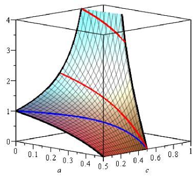
As shown in Fig. 9 the surface decreases with increasing and increases with increasing confirming that for maximizing the SCL current the singularity of the emitter should be maximal and that of the collector minimal. For the “strip/plane” lay-out and compared with the symmetric “strip” electrodes, the SCL current has doubled in value. The current can be increased further by allowing a concave collecting electrode, e.g. for the current doubles once more.
Similarly (46) valid for 2 symmetric and finite “strip” electrodes can be extended to the asymmetric case with the result
| (53) |
where the width of the emitting anode equals and that of the collecting cathode . From this equation and (37) the fields and can be obtained again up to a scale factor which can then be obtained by the condition . For the “edge/strip” lay-out with and we found . By increasing the singularity of the emitting electrode from that of an infinite “strip” to that of a line electrode the SCL current has approximately doubled. We note that the specific variation of the field components in eq. (53), has been confirmed by a more realistic numerical model for symmetric infinite “strip” electrodes [8].
The final “edge/plane” layout can be reduced to the previous case by a conformal transformation similar to what was done in section 3 and yields . Again the current can be further increased by letting the collecting electrode become concave (see Table. 1 where an overview is given of selected lay-outs).
|
|
|
|
|
|
|
|
0 | 0 | 0 | 0 |
|
|
0 | 1 | 2 | 4 |
|
|
0 | 1.94 | 3.04 | 5.12 |
7 Conclusions
We have presented a method for calculating the space-charge limited current in a 2D planar film with zero thickness between two initially coplanar electrodes. Assuming a uniform dielectric constant the current density is of the form (2) and the problem reduces to the calculation of the prefactor . In contrast with the well-known 1D Mott-Gurney law, the value of depends on the lay–out of the electrodes and can take any value between 0 and . The method gives analytical expressions for both field components in the plane of the film. Using conformal transformations the method can be extended to non planar lay-outs of the electrodes.
We found that a stable SCL current can only be sustained if, besides the space charge, the injecting electrode also induces a singularity in the field and the current increases with the strength of this singularity. In particular no stable SCL current can be sustained in a thin film with zero thickness placed between two parallel electrodes and we analyzed several limits leading to the zero current for this idealized “plane” lay-out. These results contradict previous published findings, but since these where obtained by solving the relevant equation numerically they where doomed to fail. As a second condition we noted that the singularity in the field induced by the collecting electrode should be not too strong in order for the field to remain integrable. It follows that also between idealized “edge” electrodes no SCL current can be sustained. Since the requirements for the two electrodes are conflicting, higher SCL currents can be obtained between asymmetrical electrodes and for a convex collecting electrode the maximum is obtained with an “edge” emitter and a “plane” collector, the current being 3.04 times the current between semi-infinite “strip” electrodes. The current can be increased indefinitely by allowing a concave collector.
There exist some experimental evidence for the voltage and length dependence in (3): see [8] for experiments with an organic photoconductor and [6] for experiments on a hexagonal-BN monolayer. Unfortunately since in these experiments the mobility usually is not known it’s not possible to extract a value for the prefactor. However it should be possible to compare different electrode geometries using the same layer without knowing the mobility. In particular the large polarity dependence for well chosen asymmetrical electrodes from Table 1 should be amenable to experimental verification.
Besides the electrode lay-outs considered the current can be calculated along the same lines for any lay-out which is conformally similar to one of the lay-outs considered. A further example which comes to mind is a periodic array of finite width electrodes. It is also likely, although we only illustrated it for a single example, that the shortcut introduced by Geurst [10] for calculating the field components can be applied in all those cases.
For a practical “plane” lay-out a non-zero thickness of the film must necessarily be considered. We presented two approximate numerical models to calculate the current in this case and this revealed that the current drops relatively slowly with decreasing thickness as . However since we averaged the space charge density in the direction perpendicular to the film, these results have to be confirmed by a 2D numerical model. This also holds for the other zero cases in Table 1, in particular for the practical “edge” lay-out. These might be challenging problems to solve numerically if and it remains an open question whether for those cases the limits for might be found analytically or semi-numerically.
Acknowledgment
I am grateful to Kristiaan Neyts for the stimulating and clarifying discussions on the subject of this paper.
References
- [1] M. A. Lampert, P. Mark, Current Injection in Solids, 1st Edition, Electrical Science series, Academic Press, 1970.
- [2] J. C. Ho, Organic Lateral Heterojunction Devices for Vapor-phase Chemical Detection, Ph.D. thesis, Massachusetts Institute of Technology (May 2009).
-
[3]
W. Woestenborghs, P. De Visschere, F. Beunis, G. Van Steenberge, K. A. Neyts,
A. Vetsuypens, Analysis
of a transparent organic photoconductive sensor, Organic Electronics
13 (11) (2012) 2250–2256.
doi:10.1016/j.orgel.2012.06.049.
URL http://dx.doi.org/10.1016/j.orgel.2012.06.049 -
[4]
W. Woestenborghs, P. De Visschere, F. Beunis, A. Vetsuypens, K. A. Neyts,
Transient
and local illumination of an organic photoconductive sensor, in: C. E.
Tabor, F. Kajzar, T. Kaino, Y. Koike (Eds.), SPIE OPTO, SPIE, 2013, p.
862216.
doi:10.1117/12.2000502.
URL http://proceedings.spiedigitallibrary.org/proceeding.aspx?doi=10.1117/12.2000502 -
[5]
W. Woestenborghs, P. De Visschere, F. Beunis, K. A. Neyts, A. Vetsuypens,
Detection
of a space-charge region in an organic photoconductive sensor, in:
International Display Workshop 2012/Asia Display 2012, J-Global, 2012, pp.
1855–1857.
URL http://jglobal.jst.go.jp/public/20090422/201302296559590666 -
[6]
F. Mahvash, E. Paradis, D. Drouin, T. Szkopek, M. Siaj,
Space-charge limited transport in
large-area monolayer hexagonal boron nitride, Nano Letters 15 (4) (2015)
2263–2268, pMID: 25730309.
arXiv:http://dx.doi.org/10.1021/nl504197c, doi:10.1021/nl504197c.
URL http://dx.doi.org/10.1021/nl504197c -
[7]
G. V. Dubacheva, M. Devynck, G. Raffy, L. Hirsch, A. Del Guerzo, D. M. Bassani,
Probing lateral charge
transport in single molecule layers: How charge is transported over long
distances in fullerene self-assembled monolayers, Small 10 (3) (2014)
454–461.
doi:10.1002/smll.201300502.
URL http://dx.doi.org/10.1002/smll.201300502 -
[8]
P. De Visschere, W. Woestenborghs, K. Neyts,
Space-charge
limited surface currents between two semi-infinite planar electrodes embedded
in a uniform dielectric medium, Organic Electronics 16 (2015) 212 – 220.
doi:http://dx.doi.org/10.1016/j.orgel.2014.10.036.
URL http://www.sciencedirect.com/science/article/pii/S1566119914004881 - [9] A. A. Grinberg, S. Luryi, M. Pinto, N. Schryer, Space-charge-limited current in a film, Electron Devices, IEEE Transactions on 36 (6) (1989) 1162–1170. doi:10.1109/16.24363.
-
[10]
J. A. Geurst, Theory of
space-charge-limited currents in thin semiconductor layers, physica status
solidi (b) 15 (1) (1966) 107–118.
doi:10.1002/pssb.19660150108.
URL http://dx.doi.org/10.1002/pssb.19660150108 -
[11]
A. S. Peters, The
Solution of Some Non-Linear Integral Equations with Cauchy Kernels, Tech.
Rep. IMM-NYU 307 (Jan. 1963).
URL https://archive.org/details/solutionofsomeno00pete -
[12]
O. Zmeskal, S. Nespurek, M. Weiter,
Space-charge-limited
currents: An E-infinity Cantorian approach, Chaos, Solitons & Fractals
34 (2) (2007) 143 – 158.
doi:http://dx.doi.org/10.1016/j.chaos.2006.04.006.
URL http://www.sciencedirect.com/science/article/pii/S0960077906003262 -
[13]
J. Luginsland, Y. Lau, R. Gilgenbach,
Two-Dimensional
Child-Langmuir Law, Physical Review Letters 77 (22) (1996) 4668–4670.
doi:10.1103/PhysRevLett.77.4668.
URL http://link.aps.org/doi/10.1103/PhysRevLett.77.4668 -
[14]
J. W. Luginsland, Y. Y. Lau, R. J. Umstattd, J. J. Watrous,
Beyond
the Child–Langmuir law: A review of recent results on multidimensional
space-charge-limited flow, Physics Of Plasmas 9 (5) (2002) 2371.
doi:10.1063/1.1459453.
URL http://scitation.aip.org/content/aip/journal/pop/9/5/10.1063/1.1459453 -
[15]
R. Umstattd, J. Luginsland,
Two-Dimensional
Space-Charge-Limited Emission: Beam-Edge Characteristics and Applications,
Physical Review Letters 87 (14) (2001) 145002.
doi:10.1103/PhysRevLett.87.145002.
URL http://link.aps.org/doi/10.1103/PhysRevLett.87.145002 -
[16]
J. J. Watrous, J. W. Luginsland, M. H. Frese,
Current
and current density of a finite-width, space-charge-limited electron beam in
two-dimensional, parallel-plate geometry, Physics of Plasmas 8 (9) (2001)
4202–4210.
doi:http://dx.doi.org/10.1063/1.1391262.
URL http://scitation.aip.org/content/aip/journal/pop/8/9/10.1063/1.1391262 -
[17]
M. V. Beznogov, R. A. Suris,
Theory of
space-charge-limited ballistic currents in nanostructures of different
dimensionalities, Semiconductors 47 (4) (2013) 514–524.
doi:10.1134/S1063782613040052.
URL http://dx.doi.org/10.1134/S1063782613040052 - [18] F. Tricomi, Integral equations, Dover, 1985, Ch. 4, pp. 169–171.
- [19] H. Kober, Dictionary of Conformal Representations, Dover, 1957.
- [20] K. Binns, P. Lawrenson, Analysis and Computation of Electric and Magnetic Field Problems, Pergamon Press, 1963.
-
[21]
Y. Lau, Simple
Theory for the Two-Dimensional Child-Langmuir Law, Physical Review Letters
87 (27) (2001) 278301.
doi:10.1103/PhysRevLett.87.278301.
URL http://link.aps.org/doi/10.1103/PhysRevLett.87.278301 -
[22]
J. Kunz, P. L. Bayley,
Some Applications of
the Method of Images–I., Phys. Rev. 17 (1921) 147–156.
doi:10.1103/PhysRev.17.147.
URL http://link.aps.org/doi/10.1103/PhysRev.17.147 -
[23]
S. Kumar, I. H. Sloan, A New
Collocation-Type Method for Hammerstein Integral Equations, Mathematics of
Computation 48 (178) (1987) 585–593.
doi:10.2307/2007829.
URL http://www.jstor.org/stable/2007829 - [24] F. Tricomi, Integral equations, Dover, 1985, Ch. 4, p. 171.