Transport gap engineering by contact geometry in graphene nanoribbons:
Experimental and theoretical studies on artificial materials
Abstract
Electron transport in small graphene nanoribbons is studied by microwave emulation experiments and tight-binding calculations. In particular, it is investigated under which conditions a transport gap can be observed. Our experiments provide evidence that armchair ribbons of width with integer are metallic and otherwise semiconducting, whereas zigzag ribbons are metallic independent of their width. The contact geometry, defining to which atoms at the ribbon edges the source and drain leads are attached, has strong effects on the transport. If leads are attached only to the inner atoms of zigzag edges, broad transport gaps can be observed in all armchair ribbons as well as in rhomboid-shaped zigzag ribbons. All experimental results agree qualitatively with tight-binding calculations using the nonequilibrium Green’s function method.
pacs:
73.63.-b, 72.80.Vp, 73.23.-bI Introduction & Outline
Nowadays, graphene is one of the most studied materials in condensed matter physics because of its various exceptional properties and their technical applications, see Refs. Geim, 2009; Castro Neto et al., 2009; Avouris, 2010; Novoselov et al., 2012; Katsnelson, 2012; Ferrari et al., 2015; Aoki and Dresselhaus, 2014; Foa Torres et al., 2014 for an overview. One of the most remarkable features is that graphene has a linear dispersion relation at the Dirac points, which lets the electrons behave as relativistic, massless, charged fermions. The high mobility of the charge carriers, coming from the special dispersion relation at the Fermi energy, makes graphene very promising for new electronic devices. However, the absence of a band-gap in graphene inhibits to substitute nowadays silicon-based semiconductor technology by graphene.Schwierz (2010) One approach to open a band-gap in graphene is to use nanoribbons, i.e. small stripes of graphene, see Figure 1. On one hand, this approach has the advantage that the rather small size of graphene nanoribbons may lead to a high miniaturization and integration of these devices. On the other hand, it has the disadvantage that it is still challenging to produce nanoribbons of well controlled size and geometry, although there is promising progress, see for example Refs. Cai et al., 2010; Koch et al., 2012; Ruffieux et al., 2012; Chen et al., 2013; Cai et al., 2014; Chen et al., 2015; Kimouche et al., 2015; Ruffieux et al., 2016. Moreover, connecting nanoribbons to leads, where electrons are injected and extracted, is experimentally demanding. Note also that graphene nanoribbons are predicted to operate as valley filters, see for example Ref. Rycerz et al., 2007; Nakabayashi et al., 2009; Gunlycke and White, 2011. The so-called valleytronics, where the pseudospin of the charge carriers is used, may lead to new electronic devices, which do not have an analog in silicon-based electronics.
Recently, it has been shown that a tight-binding model of graphene and polyacetylene can be emulated by microwave experiments.Bellec et al. (2013a, b); Barkhofen et al. (2013); Stegmann et al. (2017) Such experiments are well controlled and easy to perform (in comparison to experiments with real graphene or polyacetylene) and hence, offer a versatile tool to investigate in detail the properties of these systems. In this article, we study the ballistic single-electron transport through small graphene nanoribbons by microwave transmission experiments. Our measurements are supported by tight-binding calculations using the nonequilibrium Green’s function (NEGF) method.Datta (1997, 2005); Lewenkopf and Mucciolo (2013)
Graphene nanoribbons have two elementary edge structures, the zigzag and the armchair shape, see for example the horizontal edges in Figure 1 (a) and (b), respectively. Edge deformations are not considered here.Hawkins et al. (2012) Studies of graphene nanoribbonsFujita et al. (1996); Nakada et al. (1996); Brey and Fertig (2006); Wakabayashi et al. (2009, 2010) predict that armchair ribbons of width with integer are metallic and otherwise semiconducting, i.e. they show a broad band-gap at the Dirac point.111Studies using density function theory Son et al. (2006); Motta et al. (2012) indicate that also in the metallic armchair ribbons a narrow band-gap can be observed. However, these correlation effect go beyond the present study. Zigzag ribbons are predicted to be metallic for all ribbon widths. First samples of small graphene nanoribbons have been synthesized recentlyCai et al. (2010); Koch et al. (2012); Ruffieux et al. (2012); Chen et al. (2013); Cai et al. (2014); Chen et al. (2015); Kimouche et al. (2015); Ruffieux et al. (2016) indicating the predicted behavior. Here, we present emulation experiments of the electronic transport through small nanoribbons with specific edges and atomically precise connections to source and drain leads. We do not only provide further evidence to the predicted behavior but study also the effect of the contact geometry, which determines to which sites at the edges of the ribbons leads are attached. We show that by tuning the contact geometries, broad transport gaps can be induced in graphene nanoribbons with armchair and zigzag edges independent from their actual width. Contact effects on the transport in graphene nanoribbons have been addressed only rarely. Square lattices have been attached to the honeycomb lattice of graphene ribbons,Blanter and Martin (2007); Schomerus (2007); Zhang and Qin (2010, 2011); Mochizuki and Yoshioka (2009, 2010); Pieper et al. (2013) which for example induces in zigzag ribbons of even width a transport gap, while ribbons of odd width remain metallic. Similar even-odd parity effects can be observed also with respect to the total length of the ribbon.Li et al. (2008) The case where leads are attached to small Maiti (2009); Li and Zheng (2009) and larger Konôpka (2015) nanoribbons has also been studied.
The paper is organized as follows. In Section II, we describe the studied systems and explain briefly the used experimental and theoretical methods. Our results are presented and discussed in Section III. Conclusions and an outlook can be found in Section IV.
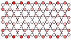
(a) armchair ribbon
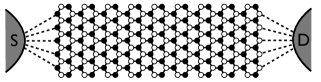
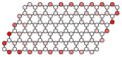
(b) zigzag ribbon (c) zigzag-rhomboid ribbon


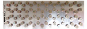
(d) photo of the microwave experiment
II System & Methods
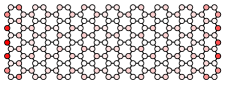
We consider graphene nanoribbons of the types shown in Figure 1, namely an armchair ribbon (a), a zigzag ribbon (b) and a zigzag-rhomboid ribbon (c). The naming of the ribbons is due to the shape of their horizontal edges and, in the case of Figure 1 (c), due to the overall shape of the ribbon. Because of experimental limitations, the length of the ribbons is kept as shown in Figure 1, while their width is varied. However, calculations have been performed also for larger systems, giving qualitatively the same results discussed below. Leads through which electron (or microwaves) are injected and extracted, are attached to the atoms at the left and right edges, see the dashed lines in Figure 1 (a).
II.1 Microwave experiment
Applying the techniques, developed to investigate the band structure of grapheneBellec et al. (2013a, b) and to emulate relativistic systemsFranco-Villafañe et al. (2013); Sadurní et al. (2013) as well as molecular systemsStegmann et al. (2017), we have performed analogous experiments to study the coherent transport in graphene nanoribbons.
A set of identical dielectric cylindrical resonators ( height, radius, refractive index ) is placed between two metallic plates. A photo of the experimental setup without the top plate is shown in Figure 1 (d). The individual resonators have an isolated resonance at , corresponding to the lowest transverse electric (TE) mode. We restrict our investigation to frequencies around , where each resonator contributes only one resonance. The nearest neighbor distance between the center of the resonators is . The dielectric resonators play the role of the carbon atoms in the ribbons, while the electromagnetic waves corresponds to the wave function of the electron. A detailed description of the experimental setup can be found in Ref. Bellec et al., 2013b. As the antennas are positioned always close to or above a single resonator they couple to the closest resonator only, thus measuring the transmission from an individual resonator on the left hand side to another individual resonator at the right hand side. By changing the antenna positions all combinations of transmission between edge resonators are measured. Due to the weak coupling of the antennas the total transmission is then given by summing up all contributions, see Section II.2. As the system is time-reversal invariant the transmission is reciprocal, i.e. the transport in both directions is the same.
II.2 Tight-binding transport calculations
Theoretically, the graphene nanoribbons are described by the tight-binding Hamiltonian
| (1) |
The coupling parameters , which have been obtained by fitting our calculations to the experimental data, are given in Table I. In the sum in Equation (1), interactions up to third nearest neighbors (3nn) are taken into account. Interactions to higher nearest neighbors can be safely ignored due to the large distance of these sites and the additional screening by the closer sites.
|
|
39.5 | 5.0 | 3.0 |
|---|
From now on we will use the normalized frequency , where the Dirac point is located theoreticallyMunárriz Arrieta (2014) in the center of the transmission band (i.e. at ).
The electron transport through the nanoribbons is calculated by means of the nonequilibrium Green’s function (NEGF) method. In the following, we briefly summarize the essential equations. Details can be found in Refs. Datta, 1997, 2005; Lewenkopf and Mucciolo, 2013. The Green’s function of the chain is defined as
| (2) |
where is the electron energy corresponding to the microwave frequency in the experiment.
The effect of the source and drain leads by which electrons are injected and extracted, is described by the self-energies
| (3) |
The coupling strength is adjusted to the experiment. The sums are over the sites where leads are attached, see for example in Figure 1 (a) the sites which are connected by dashed lines to the source and drain, respectively. The sites connected to leads are also indicated in the insets of figures 2, 4 and 5 by the black sites. The self-energies show no coherences, i.e. no off-diagonal elements, which is justified because in the experiment the antennas are coupled only weakly to the resonators.
Absorption, which is present in the experiment, is modeled by the imaginary potential (or self-energy)
| (4) |
where is the total number of sites of the ribbon. We obtain best agreement between the experimental data and the calculations using for the armchair ribbons a linear decay of the absorption , where is the width of the ribbon measured in multiples of the hexagonal cell size. For the zigzag and zigzag-rhomboid ribbons, we use a constant absorption .
In the experiment, some degree of disorder cannot be avoided completely due to the uncertainty of the resonance frequency of the resonators and the uncertainty of their positions. In the calculations, disorder is taken into account by a random potential (or self-energy)
| (5) |
where the are chosen from a Gaussian distribution which is cut at its full width half maximum, which corresponds approximately to the experimentally observed distribution and the used selection rule. We consider the standard deviation and an ensemble of realizations.
The transmission between source and drain is then given by
| (6) | ||||
where is the transmission between an individual site at the left end of the ribbon to another site at the right end. As discussed in Section II.1, these functions are measured in the microwave experiment. Note that in the last step in Equation (6), we have used the fact that the self-energies in Equation (3) describing the effect of source and drain are sparse matrices with only some non-vanishing entries on their diagonals.
In order to understand the transport properties, we will also calculate the local density of states (LDOS)
| (7) |
Due to the weak coupling of the leads to the nanoribbon, see Equation (3), the LDOS is very similar to the eigenstates of the closed Hamiltonian in Equation (1), which are near to the considered frequency. Contact induced statesGolizadeh-Mojarad and Datta (2009) have only minor effects here.
We would like to emphasize that the parameters adjusted to match the experiment and the numerics are a minimal and well defined set. Each parameter impose specific and distinct features on the measured spectra. The resonance frequency and the disk couplings (, , ) define band center, band width, and the asymmetry of the two bandsBellec et al. (2013b). The antenna coupling determines mainly the resonance depth, whereas the absorption is mainly related to the smoothing. The disorder strength takes into account fluctuation in a statistical sense, therefore a perfect agreement between experiment and numerics cannot be expected.
III Results & Discussion
III.1 Armchair ribbons
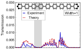
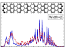
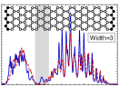
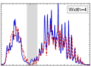
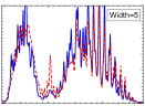
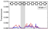
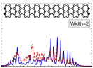
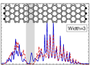
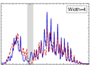
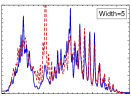
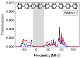
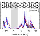
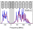
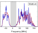
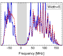
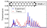
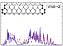
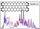
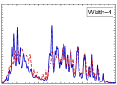
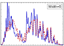
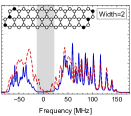
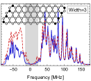
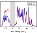
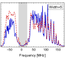
The transmission through graphene armchair ribbons for various widths and contact geometries is shown in Figure 2. Experimental data are indicated by the blue-solid curves while our tight-binding calculations are highlighted by the red-dashed curves. The narrow ribbons are sketched in the insets, where the black shaded sites are connected to leads.
We observe that in all ribbons the conductivity decreases when the Dirac point around is approached. In the first row the leads are attached to all atoms at the confining zigzag edges to the left and right. For ribbons of width with integer (i.e. widths 2 and 5 in Figure 2), the conductivity around the Dirac point is low but finite. These ribbons are metallic in the whole transmission band ranging approximately form to . For ribbons of other widths (i.e. widths 1, 3 and 4 in Figure 2) the conductivity around the band-center approaches zero. A transport gap (gray shaded regions) opens in these ribbons, which hence are semiconducting. We therefore provide clear experimental evidence of this theoretically predicted Fujita et al. (1996); Nakada et al. (1996); Brey and Fertig (2006); Wakabayashi et al. (2009, 2010); Castro Neto et al. (2009); Heikkilä (2013) behavior of graphene armchair ribbons. In general, the tight-binding calculations agree well with the experimental data. In the upper part of the conduction band (from to ) almost all resonance peaks coincide. In the lower part (from to ) the agreement is not that perfect but the general trend of the experimental data is reproduced also there. Differences between experiment and theory are more notorious in the gap than outside. In particular for certain ribbon width the experiment shows peaks which are not present in our calculations and which we attribute to localized states enhanced by irregularities of the experimental setup.
The differences between the metallic and semiconducting armchair ribbons become more pronounced if the leads are attached only to the outer atoms of the confining zigzag edges, see the second row in Figure 2. The transport through the ribbons changes drastically, if the leads are attached only to the inner atoms, as shown in the third row of Figure 2. In this case a clearly pronounced transport gap is observed for all armchair ribbons, independent from their actual width.

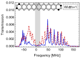
In order to understand the effects of the contact geometry on the transport, we show in Figure 3 the local density of states (LDOS), which has been calculated by means of Equation (7), near to where the transport gap appears. At the zigzag edges to the left and right, where the leads are attached, the LDOS is localized on the outer atoms, whereas it vanishes on the inner atoms. This property can be observed for all frequencies within the gap. Thus, the inner atoms on zigzag edges are essentially insulating and broad transport gaps (gray shaded regions) can be observed, if the leads are attached only to these atoms. The confining zigzag edges of the studied finite armchair nanoribbons stamp their fingerprint on the transport and can suppress the metallicity in armchair ribbons.
The behavior of the LDOS in Figure 3 can be understood by the sublattice structure of graphene.Brey and Fertig (2006); Castro Neto et al. (2009); Heikkilä (2013) At zigzag edges, see for example in Figure 1 (a) the edge to the left hand side, all inner atoms belong to one sublattice A (white resonators), whereas all outer atoms belong to the other sublattice B (black resonators). If the nanoribbon is extended hypothetically by one layer of atoms into the region, where the wave function has to vanish due to hard-wall boundary conditions, all these atoms would belong to sublattice A only. Thus, at a zigzag edge the wave function has to vanish on the sublattice to which also the inner atoms belong, whereas no constraint has to be fulfilled by the wave function for the sublattice of the outer atoms. This makes it possible that on the outer atoms of zigzag edges a edge (or surface) state can reside, while the wave function vanishes essential on the inner atoms. Moreover, the surface states are localized on one of the two points, which makes them robust against perturbations.Fujita et al. (1996); Nakada et al. (1996); Brey and Fertig (2006); Wakabayashi et al. (2009, 2010); Castro Neto et al. (2009); Heikkilä (2013) The localization of the edge states on the outer atoms of graphene zigzag edges can be understood also from a simple resonance theoretic picture as well as from valence bond and molecular orbit theory.Klein and Bytautas (1999) These edge states have been observed in microwave experiments.Bellec et al. (2014) Take into account that connecting leads to the inner atoms on the zigzag edges is not equivalent to removing the outer atoms. This would lead to beard edges, which have edge states and show different transport properties.Bellec et al. (2014) Note that we have two different origins for the observed transport gaps depending on the width of the ribbons. While for ribbons of width or the transport gap is directly related to a band gap in the energy spectrum of the system, the engineering of atomically precise contacts allows to utilize the spatial structure of the edge states and opens a transport gap in absence of a gap in the spectrum.
III.2 Zigzag ribbons
The transmission through zigzag ribbons is shown in Figure 4 (top row). The leads are attached to the inner and outer atoms of the confining armchair edges, see the black shaded sites of the nanoribbons sketched in the insets. Experimental data are shown by blue-solid curves, calculations by red-dashed curves.
As in Figure 2, the transmission decreases when the Dirac point around is approached but it remains finite for all ribbons. In agreement with theoretical predictions,Nakada et al. (1996); Brey and Fertig (2006); Wakabayashi et al. (2009, 2010); Castro Neto et al. (2009); Heikkilä (2013) all zigzag ribbons behave metallic independent from their actual width.
In zigzag ribbons a transport gap cannot be opened by contact engineering. The calculated LDOS in Figure 5 (left) close to is finite for all atoms on the confining armchair edges to the left and right hand side, because atoms form both sublattices appear there, see the alternating black and white resonators in Figure 1 (b). A surface (or edge) state does not exist at armchair edges. This behavior can be observed for all frequencies close to . Moreover, solving the corresponding Dirac equation, the wave function is located on both points (valley mixing), which makes it sensitive to perturbations.Brey and Fertig (2006); Castro Neto et al. (2009); Heikkilä (2013) Note that for the ribbons of width and , the experiment shows a small transport gap, which is up to now not understood and not observed in our theoretical calculations.
In the zigzag-rhomboid ribbons, depicted for example in Figure 1 (c), all edges have the zigzag shape. This allows to tune the transport in the system by suitable contact geometries. Close to the Dirac point the calculated LDOS in Figure 5 (right) is located on the outer atoms of the zigzag edges whereas it vanishes on the inner atoms. Therefore, if the leads are attached to the inner atoms of the edges to the left and right hand side, see Figure 4 (bottom row), a broad transport gap is observed. These gaps are observed for all ribbons independent from their size.
IV Conclusions & outlook
In this paper, the electronic transport in graphene nanoribbons has been studied by microwave emulation experiments and tight-binding Green’s function calculations. The microwave experiment emulates only the ballistic single-particle transport. Correlations due to interactions between the electrons, which may be present in real graphene, cannot be taken into account.
We have presented experimental evidence that the width of armchair ribbons determines whether the ribbon is metallic or semiconducting, see Figure 2 (top row). We have also shown that all (rectangular-shaped) zigzag ribbons are metallic, independent from their actual size, see Figure 4 (top row).
We have found that the transport properties can be tuned by the contact geometry, using the fact that the zigzag edge state resides on the outer atoms but not on the inner atoms, see the local density of states in Figure 3 and Figure 5. Hence, broad transport gaps can be induced in those ribbons, where the leads are attached to the inner atoms of zigzag edges, see the armchair ribbons in Figure 2 (bottom row) as well as the zigzag-rhomboid ribbons in Figure 4 (bottom row). The realization of such contact geometries may be extremely difficult in real graphene. However, considering the recent progress,Cai et al. (2010); Koch et al. (2012); Ruffieux et al. (2012); Chen et al. (2013); Cai et al. (2014); Chen et al. (2015); Kimouche et al. (2015); Ruffieux et al. (2016) we think that this can be possible in the near future. Our microwave emulation experiments thus may be viewed as a testing ground for new concepts.
In the future, we plan to investigate in more detail the transport in rhomboid-shaped ribbons, where the contacts are attached to the corners. For example, it has been predicted theoreticallyShimomura et al. (2011); Cuong et al. (2013) that in zigzag-rhomboid ribbons at the Dirac point the corners are conducting, while corners are insulating. This theory can be confirmed by the local density of states in Figure 5 (right). However, first experiments show surprisingly strong discrepancies to our tight-binding calculations, which we cannot explain at this point and require further studies.
Acknowledgements.
We thank N. Szpak for fruitful discussions and his comments about the manuscript. Financial support from CONACyT research grant 219993 and PAPIIT-DGAPA-UNAM research grants IG100616 and IN114014 is acknowledged. T.S. acknowledges a postdoctoral fellowship from DGAPA-UNAM. T.H.S. and J.A.F.-V. are grateful for the hospitality regularly received at the LPMC.References
- Geim (2009) A. K. Geim, Science 324, 1530 (2009).
- Castro Neto et al. (2009) A. H. Castro Neto, F. Guinea, N. M. R. Peres, K. S. Novoselov, and A. K. Geim, Rev. Mod. Phys. 81, 109 (2009).
- Avouris (2010) P. Avouris, Nano Lett. 10, 4285 (2010).
- Novoselov et al. (2012) K. S. Novoselov, V. I. Fal’ko, L. Colombo, P. R. Gellert, M. G. Schwab, and K. Kim, Nature 490, 192 (2012).
- Katsnelson (2012) M. Katsnelson, Graphene: Carbon in two dimensions (Cambridge University Press, 2012).
- Ferrari et al. (2015) A. C. Ferrari et al., Nanoscale 7, 4598 (2015).
- Aoki and Dresselhaus (2014) H. Aoki and M. S. Dresselhaus, eds., Physics of Graphene (Springer, 2014).
- Foa Torres et al. (2014) L. E. F. Foa Torres, S. Roche, and J.-C. Charlier, Introduction to graphene-based nanomaterials: from electronic structure to quantum transport (Cambridge University Press, 2014).
- Schwierz (2010) F. Schwierz, Nat. Nano 5, 487 (2010).
- Cai et al. (2010) J. Cai, P. Ruffieux, R. Jaafar, M. Bieri, T. Braun, S. Blankenburg, M. Muoth, A. P. Seitsonen, M. Saleh, X. Feng, K. Müllen, and R. Fasel, Nature 466, 470 (2010).
- Koch et al. (2012) M. Koch, F. Ample, C. Joachim, and L. Grill, Nat. Nano 7, 713 (2012).
- Ruffieux et al. (2012) P. Ruffieux, J. Cai, N. C. Plumb, L. Patthey, D. Prezzi, A. Ferretti, E. Molinari, X. Feng, K. Müllen, C. A. Pignedoli, and R. Fasel, ACS Nano 6, 6930 (2012).
- Chen et al. (2013) Y.-C. Chen, D. G. de Oteyza, Z. Pedramrazi, C. Chen, F. R. Fischer, and M. F. Crommie, ACS Nano 7, 6123 (2013).
- Cai et al. (2014) J. Cai, C. A. Pignedoli, L. Talirz, P. Ruffieux, H. Söde, L. Liang, V. Meunier, R. Berger, R. Li, X. Feng, K. Müllen, and R. Fasel, Nat. Nano 9, 896 (2014).
- Chen et al. (2015) Y.-C. Chen, T. Cao, C. Chen, Z. Pedramrazi, D. Haberer, D. G. de Oteyza, F. R. Fischer, S. G. Louie, and M. F. Crommie, Nat. Nano 10, 156 (2015).
- Kimouche et al. (2015) A. Kimouche, M. M. Ervasti, R. Drost, S. Halonen, A. Harju, P. M. Joensuu, J. Sainio, and P. Liljeroth, Nat. Commun. 6, 10177 (2015).
- Ruffieux et al. (2016) P. Ruffieux, S. Wang, B. Yang, C. Sánchez-Sánchez, J. Liu, T. Dienel, L. Talirz, P. Shinde, C. A. Pignedoli, D. Passerone, T. Dumslaff, X. Feng, K. Müllen, and R. Fasel, Nature 531, 489 (2016).
- Rycerz et al. (2007) A. Rycerz, J. Tworzydlo, and C. W. J. Beenakker, Nat Phys 3, 172 (2007).
- Nakabayashi et al. (2009) J. Nakabayashi, D. Yamamoto, and S. Kurihara, Phys. Rev. Lett. 102, 066803 (2009).
- Gunlycke and White (2011) D. Gunlycke and C. T. White, Phys. Rev. Lett. 106, 136806 (2011).
- Bellec et al. (2013a) M. Bellec, U. Kuhl, G. Montambaux, and F. Mortessagne, Phys. Rev. Lett. 110, 033902 (2013a).
- Bellec et al. (2013b) M. Bellec, U. Kuhl, G. Montambaux, and F. Mortessagne, Phys. Rev. B 88, 115437 (2013b).
- Barkhofen et al. (2013) S. Barkhofen, M. Bellec, U. Kuhl, and F. Mortessagne, Phys. Rev. B 87, 035101 (2013).
- Stegmann et al. (2017) T. Stegmann, J. A. F.-V. ne, Y. P. Ortiz, U. Kuhl, F. Mortessagne, and T. H. Seligman, Physics Letters A 381, 24 (2017).
- Datta (1997) S. Datta, Electronic Transport in Mesoscopic Systems (Cambridge University Press, 1997).
- Datta (2005) S. Datta, Quantum Transport: Atom to Transistor (Cambridge University Press, 2005).
- Lewenkopf and Mucciolo (2013) C. H. Lewenkopf and E. R. Mucciolo, J. Comput. Electron. 12, 203 (2013).
- Hawkins et al. (2012) P. Hawkins, M. Begliarbekov, M. Zivkovic, S. Strauf, and C. P. Search, J. Phys. Chem. C 116, 18382 (2012).
- Fujita et al. (1996) M. Fujita, K. Wakabayashi, K. Nakada, and K. Kusakabe, J. Phys. Soc. Jpn. 65, 1920 (1996).
- Nakada et al. (1996) K. Nakada, M. Fujita, G. Dresselhaus, and M. S. Dresselhaus, Phys. Rev. B 54, 17954 (1996).
- Brey and Fertig (2006) L. Brey and H. A. Fertig, Phys. Rev. B 73, 235411 (2006).
- Wakabayashi et al. (2009) K. Wakabayashi, Y. Takane, M. Yamamoto, and M. Sigrist, New J. Phys. 11, 095016 (2009).
- Wakabayashi et al. (2010) K. Wakabayashi, K. Sasaki, T. Nakanishi, and T. Enoki, Science and Technology of Advanced Materials 11, 054504 (2010).
- Note (1) Studies using density function theory Son et al. (2006); Motta et al. (2012) indicate that also in the metallic armchair ribbons a narrow band-gap can be observed. However, these correlation effect go beyond the present study.
- Blanter and Martin (2007) Y. M. Blanter and I. Martin, Phys. Rev. B 76, 155433 (2007).
- Schomerus (2007) H. Schomerus, Phys. Rev. B 76, 045433 (2007).
- Zhang and Qin (2010) G. Zhang and Z. Qin, Phys. Lett. A 374, 4140 (2010).
- Zhang and Qin (2011) G. Zhang and Z. Qin, Chem. Phys. Lett. 516, 225 (2011).
- Mochizuki and Yoshioka (2009) Y. Mochizuki and H. Yoshioka, J. Phys. Soc. Jpn. 78, 123701 (2009).
- Mochizuki and Yoshioka (2010) Y. Mochizuki and H. Yoshioka, Physica E 42, 722 (2010).
- Pieper et al. (2013) A. Pieper, G. Schubert, G. Wellein, and H. Fehske, Phys. Rev. B 88, 195409 (2013).
- Li et al. (2008) Z. Li, H. Qian, J. Wu, B.-L. Gu, and W. Duan, Phys. Rev. Lett. 100, 206802 (2008).
- Maiti (2009) S. K. Maiti, Solid State Commun. 149, 973 (2009).
- Li and Zheng (2009) H. Li and Y. Zheng, Phys. Lett. A 373, 575 (2009).
- Konôpka (2015) M. Konôpka, J. Phys.: Condens. Matter 27, 435005 (2015).
- Franco-Villafañe et al. (2013) J. A. Franco-Villafañe, E. Sadurní, S. Barkhofen, U. Kuhl, F. Mortessagne, and T. H. Seligman, Phys. Rev. Lett. 111, 170405 (2013).
- Sadurní et al. (2013) E. Sadurní, J. A. Franco-Villafañe, U. Kuhl, F. Mortessagne, and T. H. Seligman, New J. Phys. 15, 123014 (2013).
- Munárriz Arrieta (2014) J. Munárriz Arrieta, Modelling of Plasmonic and Graphene Nanodevices (Springer, 2014).
- Golizadeh-Mojarad and Datta (2009) R. Golizadeh-Mojarad and S. Datta, Phys. Rev. B 79, 085410 (2009).
- Heikkilä (2013) T. Heikkilä, The Physics of Nanoelectronics: Transport and Fluctuation Phenomena at Low Temperatures (Oxford University Press, 2013).
- Klein and Bytautas (1999) D. J. Klein and L. Bytautas, J. Phys. Chem. A 103, 5196 (1999).
- Bellec et al. (2014) M. Bellec, U. Kuhl, G. Montambaux, and F. Mortessagne, New J. Phys. 16, 113023 (2014).
- Shimomura et al. (2011) Y. Shimomura, Y. Takane, and K. Wakabayashi, J. Phys. Soc. Jpn. 80, 054710 (2011).
- Cuong et al. (2013) N. T. Cuong, M. Otani, and S. Okada, Phys. Rev. B 87, 045424 (2013).
- Son et al. (2006) Y.-W. Son, M. L. Cohen, and S. G. Louie, Phys. Rev. Lett. 97, 216803 (2006).
- Motta et al. (2012) C. Motta, D. Sanchez-Portal, and M. I. Trioni, Phys. Chem. Chem. Phys. 14, 10683 (2012).